High Efficiency Power Amplifiers for Modern Mobile Communications: The Load-Modulation Approach
by
 , , and
Chiara Ramella
1 ,
,
Anna Piacibello
1,
Roberto Quaglia
2,
Vittorio Camarchia
1 and
and
Marco Pirola
1,* 1
Department of Electronics and Telecommunications, Politecnico di Torino, Torino 10129, Italy
2
Centre for High Frequency Engineering, Cardiff University, Cardiff CF10 3AT, UK
*
Author to whom correspondence should be addressed.
Electronics 2017, 6(4), 96; https://doi.org/10.3390/electronics6040096
Submission received: 12 October 2017
/
Revised: 3 November 2017
/
Accepted: 9 November 2017
/
Published: 13 November 2017
Abstract
:Modern mobile communication signals require power amplifiers able to maintain very high efficiency in a wide range of output power levels, which is a major issue for classical power amplifier architectures. Following the load-modulation approach, efficiency enhancement is achieved by dynamically changing the amplifier load impedance as a function of the input power. In this paper, a review of the widely-adopted Doherty power amplifier and of the other load-modulation efficiency enhancement techniques is presented. The main theoretical aspects behind each method are introduced, and the most relevant practical implementations available in recent literature are reported and discussed.
1. Introduction
In wireless communications, much effort is put toward achieving as high data rates as possible for a given maximum transmission power and channel bandwidth. For instance (see Table 1), the challenge introduced by the 4G standard required peak data rates of approximately 100 Mbit/s for mobile access (wireless connection between a base station and a user’s handset) and up to 1 Gbit/s for the microwave backhaul (point-to-point radio links between base stations and the wired core network) [1].
In the near future, the evolution trend of wireless communication systems, with the introduction of the fifth-generation (5G) mobile standard, will demand for an increased number of applications, services, mobile devices, fixed infrastructures and smart sensors, all continuously collecting and exchanging large amounts of data through a wireless connection. Data rates exceeding 1 Gbit/s for mobile access and 10 Gbit/s for the backhaul are going to be required to reach a network capacity 10,000 higher than the current one, and this poses plenty of new design challenges at any level of the infrastructure [2,3]. This is going to be achieved by deploying a large number of smaller-sized base stations, by adopting advanced air interface solutions (e.g., multiple-input-multiple-output technology) and by exploiting also new portions of the electromagnetic spectrum, including millimetre-wave frequencies (up to 40 GHz in the initial phase). A comparison of the typical features of different generation mobile communication standards is summarized in Table 1.
This scenario suggests that wireless networks will get larger and more pervasive. Therefore, improving their energy efficiency will become a critical challenge, with an impact on both the final user experience and the environment. A major power-consuming element of any radio is the high-frequency Power Amplifier (PA), needed to boost the power level of the signal to be transmitted up to the required value. Therefore, major effort must be put toward improving its efficiency.
Power Amplifier Design Challenges
Achieving high PA efficiency is a crucial task, and it is becoming more challenging as the complexity of the adopted signal modulation schemes, centre frequencies and bandwidths are continuously increasing to comply with the requirements of next-generation communication standards. Different elements of the wireless mobile network deal with different power levels: handsets’ PAs must typically provide output powers below 1 W, while 100 W–200 W are required for a medium-sized 3G/4G base station. Microwave backhaul links below 40 GHz demand for powers up to 10 W, and similar values are expected for future small-sized 5G base stations, while a few watts may be sufficient if higher frequencies are adopted [4]. However, achieving enough power and high gain is particularly demanding at frequencies above 15 GHz. Moreover, the widespread adoption of multi-carrier modulation schemes and the continuous increase of base-band signal bandwidths are currently making it a great challenge to simultaneously obtain highly efficient and wide-band PA operation [5].
The efficiency of a PA strongly depends on the adopted device technology. Technological advances, such as the down-scaling of the transistor size and the development of device processes based on novel, better-performing materials, have played a crucial role in increasing efficiency at high operating frequency and in enabling the development of advanced amplifier architectures. This paper will be focused on medium/high-power applications at frequencies above 1–2 GHz, for which the two viable technological solutions are represented by GaAs pHEMT (pseudomorphic High Electron Mobility Transistor) and GaN HEMT processes. Despite its higher cost with respect to GaAs, GaN technology is attracting major interest, since GaN HEMTs show higher breakdown voltages, which allow them to sustain high power levels with reduced occupation area [6,7].
The maximum efficiency of a single-stage power amplifier depends on the DC power consumption and, consequently, on the bias condition of the device, which determines its class of operation [8,9]. Reduced conduction angle (e.g., Class-C), switching-mode (e.g., Class-E) and harmonically-tuned (e.g., Class-F) PAs can provide very high efficiency, but at the cost of reduced linearity. Most of the conventional high-frequency PAs adopt a Class-AB bias, in which the transistor is turned off for less than half of a cycle of the input signal, which gives an optimum trade-off between maximum efficiency and linearity [10]. It has to be noted that the different classes are able to enhance only the maximum (peak) efficiency, while their impact on back-off efficiency is limited.
The Back-Off Efficiency Issue
Current communication standards can offer high data rates in a limited frequency band thanks to the use of spectrally-efficient complex modulation schemes. Signals adopting such modulations are characterized by a very high Peak-to-Average Power Ratio (PAPR), meaning that the time domain waveform presents rare peaks significantly higher than the average value, as shown in Figure 1. The PA efficiency is determined by the average output power. However, not to compromise the quality of the carried information, the PA must be also highly linear, introducing limited distortion on the output signal. Practically, the PA must not clip the signal peaks, meaning that the maximum output power of the PA must be around PAPR times larger than the average one. Crest-reduction techniques [11,12,13] can be applied to partially overcome this limit, at the cost of an increased non-linear behaviour.
Figure 2 reports the efficiency of a conventional Class-AB PA along with the probability density functions of three different modulated signal, as a function of Output power Back-Off (OBO), which is the amount of output power reduction with respect to the maximum. Class-AB efficiency is monotonically increasing as a function of the output power: if the average power of the signal to be amplified is reasonably close to the maximum one (low-PAPR signals, e.g., GSM), the amplifier exhibits good average efficiency. However, in the case of high-PAPR signals (e.g., LTE), the PA works most of the time at high OBO levels with an efficiency (back-off efficiency) that is only a small fraction of the maximum value.
2. Back-Off Efficiency Enhancement Techniques
For a given bias point, a power device works at its maximum efficiency when both the output voltage and current swings are maximized. These swings are set by the load termination and the drain bias voltage as:
and can be visualized as a dynamic load line. Therefore, for a given power level, i.e., for a given , an optimal load line does exist where the amplifier is yielding its maximum efficiency. To ensure high efficiency at any possible back-off level, the load line should be dynamically changed as a function of the input power. As shown in Figure 3, this can be done either acting on the load resistance or on the drain bias voltage, yielding two possible back-off efficiency enhancement approaches: load modulation and bias modulation [8].
The most popular load modulation solutions are the Doherty power amplifier [14] and the Chireix outphasing amplifier [15]. Concerning bias modulation, the Envelope Elimination and Restoration (EER) technique, also known as the Kahn technique [16], and the Envelope Tracking (ET) [17] technique are currently attracting major interest. More recently, advanced variations and combinations of these techniques, such as asymmetric multilevel outphasing [18], have been also reported.
Other efficiency enhancement techniques that fall outside this classification also exist [8], among which the most renowned is the Sequential Power Amplifier (SPA) [19,20,21,22,23].
The various efficiency enhancement solutions can be also classified according to their practical implementations. It is possible to distinguish between fully-analogue and mixed-signal solutions, where the latter includes both analogue and digital circuits. Another distinction can be made between PA-level and system-level solutions. In the former case, the high frequency PA structure is modified to be more efficient, without requiring a change of functions in the other parts of the transmitter. In the latter case, a classical high frequency PA is made more efficient by modifying the parts of the system that manage the PA. In reality, this distinction is never sharp, and efficiency enhancement is achieved acting on both levels. For example, the great success of Doherty has been enabled by the introduction of the new 4G base stations, where the overall transmitter has been slightly modified in order to maximally exploit the capabilities of the Doherty Power Amplifiers (DPAs) employed to replace the old class AB PAs [24]. In the future, as communication systems will continue to move towards signals with increasingly high PAPR, the most effective solutions will probably imply deeper modifications of both the PA and the overall transmitter, acting on both loading and biasing conditions of the PA, while moving toward a massive involvement of cost-effective digital elements for signal manipulation (e.g., predistortion and/or equalization).
In this paper, different load modulation techniques are presented and discussed, highlighting their potential advantages and drawbacks. Without detailing any proposed variation, an overview of the most relevant/recent research topics related to these techniques is presented. The Doherty PA will be analysed more deeply, it being, at present, the most studied and adopted solution.
3. Doherty Power Amplifier
The Doherty Power Amplifier (DPA) is named after its inventor W. H. Doherty, who first proposed this architecture in 1936 [14]. The DPA scheme is illustrated in Figure 4: the Auxiliary (or Peaking) amplifier acts basically as an active load for the Main (or Carrier) amplifier.
In the basic DPA scheme, the Main amplifier is a Class-B or Class-AB amplifier (Class-AB is preferred for its higher linearity [9]). However, it is designed to keep its maximum output voltage swing, and thus its maximum efficiency, for any input power level between the so-called break point and the maximum. In the classical DPA implementation the Main maximum current contributes to half of the maximum total current, which sets the break point at 6 dB OBO. The Auxiliary device is off for input powers below the break point value and is turned on when input power increases above this level. When active, it injects current into the common load, contributing to the total output power and modulating the load seen by the Main amplifier.
The DPA behaviour can be therefore split into two different regions: (1) the low-power region where the Auxiliary device is off and (2) the Doherty region where both devices are on. The simplified output section of a DPA in the two operating regions is depicted in Figure 5. Active devices in common-source configuration behave in first approximation as current sources up to saturation. In the low-power region (Figure 5a), ideally, only the Main device is contributing to the output, while the output impedance of the Auxiliary device is an open circuit. The efficiency increases as power increases as for a Class-AB PA (Figure 6, red curve). At the break point, the Main device drain voltage reaches its maximum swing and cannot increase any further, and the Auxiliary turns on. In the Doherty region (Figure 5b), both PAs contribute to the output power. The impedance seen from the output section of each branch is increased by the current contribution of the other stage:
In particular, varies from (low-power region) to (saturation), while goes from an open circuit to , where in the classical DPA, , being the optimum load resistance of the Class-AB PA. Indeed, a decrease of is needed to keep the Main device working at maximum efficiency; therefore, on the Main branch, an Impedance Inverting Network (IIN), which is typically a quarter-wavelength line, must be added for proper load modulation.
The IIN transforms an impedance at one end to an impedance proportional to at the other end, hence the name. As a consequence, the increase of due to is transformed into a decrease of the impedance seen at the Main drain plane. This permits, for increasing drive, maintaining a constant (hence the use of a voltage source in Figure 5b), which results in constant maximum efficiency in the Doherty region (Figure 6, red curve).
In an ideal DPA, the impedance trajectories followed by the two modulated loads are represented on the Smith chart as straight lines lying on the real axis, i.e., for any given power, the load seen by both PAs is purely real.
Note that the IIN introduces a 90 phase difference, which must be compensated for in order to maintain the proper phase relation between and and sum them constructively at the output. This is typically done either inserting a 90 delay line at the input of the Auxiliary amplifier (as in Figure 4) or adopting a hybrid 90 coupler as the input power splitter.
In the Doherty region, the Auxiliary amplifier also contributes to the output power, with an efficiency that increases with power (Figure 6, blue curve). At the maximum input power level, the efficiencies of both amplifiers are maximum, and they contribute equally to the output power, which is therefore 6 dB higher than that at the break point (3 dB more from the Main and 3 dB from the Auxiliary). The overall efficiency is reported in Figure 6, black curve.
In the original Doherty formulation, also the Auxiliary amplifier was biased in Class-B, and it was turned on and off by some external circuitry. However, the implementation of such a control circuit still represents an issue. A simple strategy to overcome this issue is to bias the Auxiliary in the Class-C condition: at low input power, the device is naturally off, while with the proper selection of bias voltage, it can turn on automatically when the input power reaches the threshold. This architecture is the most adopted, and it is referred to as the Class-AB/C Doherty PA [9]. However, it is affected by some drawbacks, the most evident being that Class-C amplifiers provide less current than Class-B or -AB ones. Therefore, in order to have equal maximum currents at saturation, either an uneven input power splitter [25] or two different device sizes [26] (the Auxiliary being the larger one) must be adopted. Moreover, Class-C biased transistors suffer from lower power gain and worse linearity due to higher power-dependent gain variations.
The DPA efficiency can be further improved by enhancing the efficiency of both the Main and Auxiliary amplifiers adopting some harmonic tuning approach. For example, a second-harmonic control strategy for the Main amplifier enabling wide-band operation is demonstrated in [27], while in [28], a Class-F amplifier is adopted as the Main device. More recently, a high-efficiency switched-mode Class-E/F amplifier is employed in [29] to implement both the Main and the Auxiliary cells, while in [30], the efficiency of the Auxiliary stage is enhanced by using input harmonic loading. In [31,32], two extremely compact output combining networks integrating harmonic load terminations are proposed, based on a lumped-element and a harmonic-trap network, respectively. As a final example, in [33], the odd harmonics generated in the Auxiliary amplifier are exploited to shape the drain voltage waveform of the Main device allowing it to operate at a reduced supply voltage, thereby increasing efficiency.
3.1. Doherty PA Limitations
The Doherty architecture suffers from two main limitations in terms of back-off and bandwidth. Moreover, practical DPA implementations present other issues, in terms of operating frequency and linearity, due to device non-ideality. All these aspects will be discussed in the following, introducing the most relevant fully-analogue solutions proposed in the literature. In Section 3.2, how these issues can be solved by resorting to digital solutions will be discussed.
3.1.1. High-Efficiency Power Range
The standard DPA is able to provide an efficiency peak at 6 dB OBO or, in other words, a High-Efficiency Power Range (HEPR) of 6 dB. However, the increasingly high PAPR of modern modulation schemes pushes towards deeper back-off levels, up to 12 dB, which are difficult to achieve with this solution.
The basic way to improve the HEPR is adopting an Auxiliary device larger than the Main one. For example, a break point at 12 dB OBO is achieved if the Main amplifier reaches its maximum voltage swing at 1/16 of the maximum output power. It can be shown that ; thus, the Main amplifier delivers at maximum 1/4 of the maximum output power, while the remaining 3/4 must be provided by the Auxiliary, which should therefore be at least three-times larger than the Main (assuming Class-C bias and uneven power splitting) [34]. This solution is known as asymmetrical DPA [35,36,37,38]: the higher the level of asymmetry, the wider the HEPR. On the other hand, increasing asymmetry causes a severe gain reduction, due to the stronger influence of the inherently lower gain Class-C Auxiliary stage on the overall performance and to the reduced power delivered to the Main stage. Moreover, it poses practical limitations on the design of the input power splitter, whose line width is increasing with the splitting ratio. Finally, also the design of the input matching, stabilization and bias networks becomes less straightforward in the case of different devices. The asymmetrical DPA solution is therefore only viable for medium HEPR, below 10 dB.
In [39], an interesting combination of the asymmetrical DPA and the sequential PA solutions is proposed, achieving 10 dB HEPR. In this case, the load modulation effect is used to achieve a smoother transition from the low-power condition, where only the Main is on, to the high-power condition, where only the Auxiliary is on.
An alternative approach for the HEPR issue is the multi-way/multi-stage DPA architecture [40,41,42,43]. The multi-way DPA, or N-way DPA, is a variant of the asymmetrical DPA where the single Auxiliary stage is replaced by parallel devices that turn on simultaneously, realizing an equivalent larger Auxiliary device, overcoming the issues related to the adoption of single very large devices. The efficiency, however, suffers a sensible drop in the Doherty region as shown in Figure 7, left. The multi-stage DPA, or N-stage DPA, replicates the Doherty concept in a cascade configuration: it also has Auxiliary stages, but they turn on separately, following a precise scheme, in order to provide N efficiency peaks and Doherty regions as shown in Figure 7, right. The main drawback of both of these solution is the increased circuit complexity, requiring N-way splitting circuits and complex output power combining networks, especially in the case of the N-stage DPA.
To keep the increased circuit complexity at the minimum, different solutions to increase the HEPR while still maintaining a two-stage symmetrical DPA structure have been proposed. For example, in [44,45,46,47], an approach adopting asymmetrical drain bias voltage is presented. The main drawbacks of this solution are device under-utilization and increased bias circuit complexity. In [48] and [49], instead, a wide HEPR for a symmetric DPA is achieved by modifying the output power combiner, thus ensuring a high power utilization for both transistors, while in [50], electronically-tunable devices are adopted to dynamically adjust circuit parameters as a function of the average input power level, maintaining high efficiency even in deep OBO conditions. A novel technique for enhancing the HEPR of traditional symmetrical DPAs, based on adopting an output impedance for the Auxiliary stage different from an open circuit and changing the phase delay of the IIN, has been recently proposed in [51].
3.1.2. Linearity and Efficiency Drop
The DPA theory is based on the simplified assumption of two devices working as ideal voltage-controlled current sources. When accounting for device parasitic elements and other non-idealities, several practical issues arise. In addition, the different bias conditions of the Main and Auxiliary devices result in different output current profiles, which in turn yield gain imbalance and phase offset between the two stages. As a consequence of all these factors, a deviation from the optimum load modulation, a back-off efficiency drop and poor linearity arise.
Parallel parasitic losses of the Main PA, together with its non-zero knee voltage, impacts DPA back-off efficiency, limiting the maximum value actually achievable. Both of these factors are determined by device technology. Whereas the knee voltage limitation can be mitigated, e.g., by referring to the design strategy presented in [52], device parasitics represent a major issue, which is hard to overcome at the PA design level.
The impossibility of having an abrupt turn-on of the Auxiliary PA poses a challenge in the bias design. Adopting an early turn-on, in fact, mitigates gain imbalance between the two stages and output current waveform distortion, thus improving DPA linearity. Moreover, it may extend the HEPR to higher OBO values, but, on the other hand, it sensibly lowers the efficiency peak. As a consequence, a careful design of the turn-on power level to trade-off between linearity and back-off efficiency is mandatory.
Reactive device parasitics have a major impact on the DPA load modulation. A proper load modulation requires that any real impedance variation at the load reference plane be transformed into a corresponding real impedance variation at the intrinsic drain plane of the two devices. Moreover, in the low power condition, when the Auxiliary device is off, the open-circuit condition at its drain plane must be as close to the ideal as possible and correctly restored at the common load plane, to avoid current leakage from the Main device. In the ideal DPA, only real impedances are involved, and therefore, the quarter-wavelength IIN classically adopted can correctly perform load modulation. However, when dealing with a real device, its output parasitic reactances add an imaginary part to the load seen at the device drain plane that must be compensated. This is done by the device output matching network (see Figure 8), which is however designed only for one specific load impedance value, typically the value at saturation. This means that for all other impedance values explored by load modulation, the reactive parasitics are not properly compensated, and an unwanted phase rotation affects the load modulation [53], resulting in lower back-off efficiency peak and worsening of the DPA linearity.
The most common solution to restore optimal load-modulation behaviour is the offset lines technique, introduced in [54] and depicted in Figure 8. In [53,55], it is demonstrated how the insertion of two transmission lines, with characteristic impedance equal to the load impedance at saturation and of proper length, placed at the output of both the Main and Auxiliary devices, can improve load modulation, and thus both linearity and efficiency. In particular, the offset line at the output of the Auxiliary amplifier forces the necessary almost-ideal open-circuit condition at low power levels, while the one at the output of the Main stage keeps under control the load matching within the whole Doherty region, thus maximizing the power efficiency.
An alternative method to compensate for parasitic effects, which is nowadays often preferred to offset lines, is the co-design of the device output matching networks and output combiner, where the correct load modulation is imposed as an additional constraint for circuit optimization [56,57,58]. This approach has the advantage of reducing the circuit size. On the other hand, the offset lines technique enables one to easily insert already existent PAs in a Doherty configuration. Both of these techniques are compatible with wide-band applications. Bandwidth enhancement is obtained by means of dual-band offset lines in [59] and with a wide-band output compensator in [27]. More recently, the co-design technique has been further enhanced by adopting a black-box approach for the entire output combiner, thus eliminating the limitation imposed by the presence of the quarter wavelength impedance inverting network. In this way, the phase difference between the two branches becomes an additional degree of freedom and can be optimized in order to achieve better efficiency and linearity, as in [60], to enhance HEPR as in [48], or to improve the bandwidth as described in [61], where the analytical analysis of this novel approach is introduced, presenting a technique for wide-band power combiners’ design that can be applied both to Doherty and to Chireix PAs (Section 4).
An alternative method to solve the device parasitics issue is to use the non-linear embedding technique. This technique, firstly introduced in [62,63], has been recently applied to the design of a high-HEPR, asymmetric DPA [45]. Following this approach, the optimum harmonic terminations for the best DPA performance are designed at the intrinsic drain plane or, equivalently at low frequency, where device parasitics are negligible. In this way, waveform engineering (i.e., the optimization of the current and voltage waveforms) can be directly implemented. Then, the non-linear embedding technique is used to synthesize the multi-harmonic terminations to be presented at the extrinsic output plane (after parasitics) to achieve the desired PA behaviour.
In a real device, both the transconductance and the intrinsic capacitances (in particular the equivalent input capacitance) are not constant, but vary as a function of the input power, thus affecting the phase alignment of the output currents. Moreover, the capacitance variations are larger in case of the Class-C biased device, further enhancing this undesirable effect.
This power-dependent phase mismatch, in turn, disturbs the load modulation, preventing a correct load matching at all power levels, and leads to severe power loss and output phase distortion (AM/PM Amplitude-Modulation-to-Phase-Modulation distortion), thus affecting both DPA efficiency and linearity.
Several different solutions have been proposed so far to compensate for this phase variation. For example, in [55], two additional offset lines are adopted to enhance back-off efficiency, while in [64], it is shown that a properly designed offset line added at the Auxiliary input can improve linearity of the DPA. In [65], it is demonstrated that the use of an extended-resonance input power divider yields an adaptive input-dependent power division between the Main and Auxiliary stages, compensating the phase misalignment and thus enhancing both linearity and efficiency.
Even if linearity improvements have been achieved by resorting to different solutions, the overall linearity of DPAs is still incompatible with standard telecommunications requirements. In particular, a major issue is the unavoidable AM/PM distortion due to the load modulation [66,67,68]. The adoption of Digital Predistortion (DPD), or other linearization techniques, is therefore mandatory in many application of the DPA [69,70,71,72,73]. The additional power consumption and circuit complexity required for linearization raise an open question about the actual cost effectiveness of the combined DPD + DPA transmitter: while its superiority with respect to conventional transmitters has been proven in base-station applications, its applicability to point-to-point backhaul radio networks is still not clear [24,25]. Similar concerns apply for the adoption in large antenna array systems, as the ones foreseen in 5G base stations, where the output power of each PA is not very high and, similarly to the backhaul case, the non-linearity of the DPA might result in being too strong to be accounted for by simple pre-distorters.
3.1.3. Bandwidth
At present, a major challenge in DPA design is to increase its bandwidth. The bandwidth of a PA can be referred to by different features. In conventional PAs, either the output power or the power gain is adopted to define the bandwidth. However, since DPAs are used to increase back-off efficiency, a useful definition of bandwidth is, in this case, the range of frequencies for which the back-off efficiency peak remains close (e.g., within 10%) to the maximum value achieved at centre frequency. There are several factors impacting the attainable DPA bandwidth: the most evident are the quarter-wavelength IIN and the offset lines (where used), which are frequency-limited networks in nature. Moreover, if not properly designed, also the input and output matching networks may result in being too narrow-band, limiting the overall DPA bandwidth. However, in practical DPAs, the limits imposed by these networks are hardly reached, since bandwidth is actually defined by the devices’ output capacitances. In fact, as frequency moves away from the centre (design) value, the impedance seen from the Main drain at back-off deviates from its optimum value due to parasitic effects, and load modulation in the Doherty region results in being sensibly different from the theoretical one [74,75].
An effective method to reduce the limiting effect of the devices’ output capacitances is to account for them within the combining network [76]. This approach has the main advantage of minimizing circuit size, with noticeable bandwidth enhancements [27,46,58].
Beyond this, the use of non-conventional output combiners [77,78,79] or the application of the real frequency technique [80] to the design of the output matching networks [75] is proven to be able to further improve DPA bandwidth. In the modified DPA proposed in [46,81], enhancement of DPA bandwidth is obtained by modifying the characteristic impedance of the IIN transformer. In fact, frequency limitation arises when the load seen by the quarter wave transformer is different from its characteristic impedance, which, in the traditional DPA architecture, matches the load value at saturation, which is . This clearly means that in back-off, where the output load is , impedance mismatch occurs (at the plane of Figure 5b). A wider bandwidth can be achieved by forcing the impedance matching condition to be satisfied in back-off instead. In this way, the frequency-dependent mismatched condition is moved away from the break point toward saturation where, however, the compressive behaviour of the saturated PAs ensures smaller sensitivity. The main advantages of this technique are a more favourable impedance transformation ratio for the design of the output matching networks (since needs to be increased) and the possibility of adopting the same device for both the Main and Auxiliary stages. On the other hand, its major limitation is the need for asymmetrical drain bias and the consequent under-utilization of the Auxiliary device. In [82], a similar approach is proposed for a DPA that includes offset lines. In this case, the characteristic impedances of both the IIN and of the Main offset lines is set equal to the output load at back-off, while that of the Auxiliary offset line is kept equal to the output load at saturation, also achieving bandwidth enhancement.
Not all of the cited techniques deal with the limited bandwidth of the IIN itself, which can be improved by replacing the quarter-wavelength line with inherently wider-bandwidth implementations, such as the Klopfenstein taper proposed in [81].
3.1.4. Frequency
All the discussed DPA limitations tend to become more severe as centre frequency is increased, due to device gain degradation and higher losses [83]. At present, watt-level working DPA examples are limited to Ku-band (below 18 GHz) for implementations in the most widely-available 0.25 m gate-length GaAs [84] or GaN [58,85] technologies. Few examples of watt-level DPAs working in the K-band (below 27 GHz) are also available, resorting to more performing 0.15 m GaAs [86] or GaN [87] gate-length technologies, while, above K-band power, levels around 0.5 W are proven to be attainable in [88,89] also resorting to 0.15 m GaAs pHEMTs. These examples indicate that technological advancements in compound semiconductor processes are crucial to allow for the application of the DPA architecture to next-generation communication systems.
3.2. Digital/Dual-Input DPA
Recent developments of Digital Signal Processing (DSP) and Digital-to-Analogue Conversion (DAC) techniques make increasingly attractive mixed-signal solutions previously considered unfeasible. In this framework the digital DPA is emerging as a promising solution able to overcome the typical issues of the analogue DPA [90]. In a digital DPA, two separate Radio Frequency (RF) inputs for the Main and Auxiliary amplifier are separately generated and controlled for optimized DPA performance, as shown in Figure 9, hence the alternative name of dual-input DPA.
In the dual-input DPA, the signal-conversion block is duplicated, which implies higher cost and complexity, but the input analogue splitter, which is a crucial element to design, is eliminated. Most importantly, signal splitting between Main and Auxiliary can be digitally adapted in several ways to enhance a particular DPA’s performance.
At present, concurrent optimization of different DPA features (efficiency, linearity, bandwidth) is still not demonstrated; however, it is possible to reconfigure the optimum splitting scheme, according to the peculiar system requirements.
In [55,91], it is shown how to enhance back-off efficiency through adaptive power distribution and phase alignment algorithms, ensuring minimized wasted power when the Auxiliary device is off, as well as phase-aligned output currents during load modulation. In [92], the HEPR is improved by dynamically adjusting the amplitude and phase of the input signal of the two amplifiers, and three-input versions also exist [93] for further HEPR enhancement. An even signal distribution in the low power region, together with an uneven one in favour of the Auxiliary in the Doherty region, is optimum for linearity and flat-gain response [94], while a frequency-dependent signal decomposition scheme is proposed in [95] to improve DPA bandwidth. A further bandwidth enhancement is obtained in [96], by resorting to a digital equalizer, and in [97], where instead, a mixed DPA-outphasing dual-input architecture is proposed. Recently, in [98], a wide-band dual-input Doherty was demonstrated, relying on a quasi-MMIC (Monolithic Microwave Integrated Circuit) technology, with the IIN realized as a high-pass filter to minimize the components’ count and the inductor losses.
Beyond the additional cost, power consumption and circuit complexity of the digital processing, the main limitation of the digital DPA is the need for precise alignment and isolation between the two input signals.
4. Chireix Outphasing Power Amplifier
The term outphasing power amplifier comprehends a wide variety of architectures, all exploiting the combination of Phase-Modulated (PM) signals with equal constant amplitude to achieve amplification of an Amplitude-Modulated (AM) input signal. The scheme of a basic two-stage single-input single-output outphasing PA is illustrated in Figure 10: the input Signal Component Separator (SCS) network translates the AM signal into two constant-envelope PM signals with opposite phase. After amplification, the output network recombines them, so that the original amplitude modulation is retrieved on the load. Since the two branch PAs work with signals having a constant envelope, they can be operated in highly saturated, partially-switching or fully-switching modes to provide very high efficiency [8]. As a result, linear amplification of the input signal is achieved using non-linear building blocks, which is commonly referred to as Linear amplification using Non-linear Components (LINC) [99].
The two branch PAs work at constant output power, and thus, they need to be loaded with a constant load equal to the optimum resistance. To achieve this goal, classical outphasing PAs adopt an isolating power combiner, which yields high efficiency only at maximum output power. In power back-off conditions, all the unnecessary output power from the branch PAs is wasted at the isolating port of the output combiner [100,101]. A possible way to improve efficiency is therefore to rectify the non-used power at the isolated port and reuse it for device bias [102]. However, with this approach, the impedance variation at the isolated port produces an undesired load modulation effect on the two PAs, with negative impact on their efficiency. In fact, load modulation can improve PA efficiency only if the impedance variation trajectory is properly conceived for this purpose; otherwise, it can worsen it even considerably.
In 1935, Chireix proposed a substantial modification to the outphasing scheme, introducing a proper load modulation effect by means of a non-isolating output power combiner. This strategy allows for a significant improvement of the back-off efficiency, while maintaining the high linearity typical of the outphasing architecture. However, it sensibly increases the circuit design complexity.
To explain the load modulation effect in a Chireix outphasing PA, the simplified circuit of Figure 11a is considered. It represents the output section only of the Chireix PA where the two amplifiers are replaced by ideal voltage sources, feeding signals with equal amplitude V and opposite phase () into a differential load R connected in series between them. Each PA varies the load seen by the other according to the value of the outphasing angle as:
When , the output power is maximum and a purely resistive load () is seen by both PAs. When , the output power is null and the loads are two open circuits. For intermediate power levels, the load impedance of the two branch PAs moves along a constant resistance semicircle as shown in Figure 12a.
The load trajectories in Figure 12a cross the real axis only for and , while for all other values of the outphasing angle, both load impedances show a significant imaginary part. As a consequence, the overall efficiency decreases with , yielding no substantial improvement to back-off efficiency. A second efficiency peak can be forced at a defined OBO level, by adding two shunt-compensating reactive elements, with equal and opposite susceptance , as in Figure 11b, that resonate out the equivalent susceptance seen by each amplifier for a specific value of the outphasing angle , i.e.,
Under such a condition, the load trajectories of the two branches cross the real axis for as shown in Figure 12b, which results in an OBO efficiency peak as shown in Figure 13, which reports the efficiency curves versus OBO for different values of the compensating susceptance, i.e., for different HEPRs. These curves are theoretically derived by analysing the simplified Chireix equivalent of Figure 11b and assuming perfectly sinusoidal output voltages along with half-rectified sinusoidal drain currents. It is to be noted that the compensating susceptance also changes the position of the high-power efficiency peak, which is no more at 0 dB OBO.
Each case is compared to the analogues Doherty curve. Interestingly, the shape of the efficiency curve of the Chireix outphasing changes depending on the desired OBO optimization point. It is similar to that of a Doherty, with two peaks of equal value, when the compensation is designed for deep back-off (9 dB in the example). On the contrary, if a relatively low OBO value, such as 3 dB, is selected, the two peaks are no longer distinct, and the curve presents a unique wide plateau. This condition corresponds to the intersection points of the load trajectories (see Figure 12b) moving closer to each other, until the two semicircles become almost tangent to the real axis. On the other hand, this results in larger distance between the high-power efficiency peak and the 0 dB OBO point, i.e., to a lower efficiency at maximum output power.
The theoretical efficiency curves suggest that the Chireix outphasing architecture can give potentially better HEPR performance than the standard DPA, since back-off efficiency is maintained higher in between the two peaks even when they are far apart. Furthermore, a key advantage of the Chireix outphasing topology is the major flexibility in reconfiguring the OBO efficiency peak: in fact, the design of the two branch PAs can be carried out independently of the desired HEPR, since it is fully determined by the compensation susceptance. Finally, as in any outphasing architecture, the Chireix PA has a potentially very good linearity, thanks to the fact that the branch PAs are operated at a fixed output power.
4.1. Chireix Outphasing PA Limitations
Despite its potentially high performance, the Chireix PA is much less exploited by industry and research than the Doherty PA. The main limitations for a practical implementation of a Chireix PA are represented by the deviation of a real transistor behaviour from that of an ideal voltage source, typically assumed for Chireix PA theoretical analysis. Furthermore, there are several practical issues related to the realization of the output combiner and of the input network, in charge of generating the two opposite phase modulated signals from the amplitude modulated one at the input. Moreover, the Chireix architecture suffers from inherently low power added efficiency, high thermal stress, possible stability issues and bandwidth limitations, as discussed in the following.
4.1.1. High Efficiency Power Range and Stability
From Figure 13, the HEPR of the Chireix outphasing seems to be rather good. Moreover, similarly to the Doherty PA case, the HEPR can be further enhanced by adopting multi-way/multi-stage architectures [103], while even better results are obtained by combining the outphasing architecture with other back-off efficiency enhancement techniques, such as the supply-modulated outphasing PA [104] or the Doherty-Outphasing PA [97,105,106].
However, a closer look at the load trajectories of Figure 12b reveals a potential issue of the Chireix architecture: the larger the desired HEPR, the wider the distance between the two points where the trajectories cross the real axis and the wider the semi-circle that joins these points. As a consequence, the wider the HEPR, the wider the output power range for which the load seen by the two amplifiers has a very large reactive component, which affects PA performance. Highly reactive loads pose severe issues on efficiency, due to reactive current losses, and on stability. In fact, oscillation may occur for certain loading conditions, especially when loads are close to open circuit [34].
4.1.2. The Voltage Source Issue
The main reason why practical realizations of Chireix outphasing PAs hardly show efficiency curves that resemble the theoretical ones is the very strong assumption that the branch amplifiers behave like voltage sources.
An RF transistor works quite closely to an ideal voltage source only when in a highly saturated state. Therefore, the branch PAs inputs must be overdriven to keep them working at a fixed high output power, for different input power levels. This severely worsen its Power Added Efficiency (PAE), especially when large HEPR are required. The PAE, in fact, accounts also for the input power, which must be kept reasonably high in the entire power range for which high efficiency (i.e., proper saturated operation of the branch PAs) is desired. Moreover, working constantly at high output power exposes the transistors to possible thermal stresses [8].
For a successful implementation of outphasing PAs, it is crucial to find novel solutions for realizing PAs where the adopted transistors behave as good voltage sources without over-driving, which is still a key challenge, especially in high power compound semiconductor technologies like GaAs and GaN. Recent attempts to design voltage-mode Class-D GaN PAs can be found in the literature [107,108]. However, most realizations of GaN outphasing PAs are currently based on saturated Class-B [101,109] or on Class-F PAs [110,111,112], with consequent sub-optimal efficiency curve.
In [113], it is shown how to overcome this issue combining the non-linear embedding technique and a novel Chireix structure, where the current-generator-like behaviour of the branch PAs is transformed into the desired voltage-generator-like one by using two offset lines and two ideal transformers.
4.1.3. Bandwidth
The Chireix PA is based on resonating out reactive components. This clearly implies an inherent bandwidth limitation, due to the frequency-dependent nature of the reactive compensating elements.
Nevertheless, similarly to the case of the Doherty PA, the actual bandwidth limiting factors of practical PA implementations are related to the transistor parasitics and the output combiner. The simplified topology shown in Figure 11, with the load connected in series across the two branches, is not practically realizable since most of the high frequency systems use single-ended loads and are connected through coaxial cables. Therefore, a transformation from a balanced configuration to an unbalanced load is required, e.g., with a balun [34]. In Figure 14, an example of how this balun combiner can be realized is shown. In the original version, Chireix proposed the use of two quarter-wavelength transmission lines sections joining at the output [15,100] (see Figure 14a), while in [114,115], a Marchand balun (see Figure 14b) and a transformer (see Figure 14c) are used, respectively.
As for the case of the Doherty PA, it is demonstrated in [61] that a black-box approach for the design of the output combiner, relying on load-pull measurements/simulations and on proper optimization of the combiner network parameters, can yield a reduced-complexity circuit and optimum Chireix PA performance over wide frequency ranges.
4.1.4. Single-Input Architectures
The input network in charge of performing power splitting and AM-to-PM conversion (see Figure 10) can be realized either in the analogue or digital domain. Most of the Chireix PA solutions available in the literature exploit a separate digital control of each branch PA, in a configuration similar to that of Figure 9 (with two identical PAs and a Chireix output combiner). Despite the unavoidable duplication of the several signal conditioning blocks and the consequent increase in cost and complexity, the digital handling of the input section of the Chireix PAs allows for a huge simplification in the PA architecture. AM-to-PM conversion is in fact a major challenge for analogue implementation, while it becomes quite simple with digital control where the most appropriate input driving conditions can be selected, both in magnitude and phase, at each operating frequency.
However, one of the reasons behind the commercial success of the Doherty PA is its fully-analogue nature, which allows for a direct replacement of traditional PAs within an existing transmitting system. Consequently, part of the recent research on the Chireix PA is focused on achieving fully-analogue single-input architectures of reasonable complexity. The basic idea behind all the proposed solutions is to synthesize the input section as the dual of the output section. This concept, founded on the principle of time-reversal duality [116], is illustrated in Figure 15. Following this approach, the Chireix output power combiner is modelled as a Resistance Compression Network (RCN) [117]. This class of networks, whose basic scheme is shown in Figure 16, allows for a direct derivation of the input network as a particular RCN, terminated with non-linear components . These components should have an effective resistance that depends on the input power, according to an appropriate law. These non-linear variable resistances can be practically realised exploiting either a diode-based network [112] or the intrinsic input impedance variation with the drive level that affects non-ideal active devices [118].
5. Dynamic Load Modulation
The Dynamic Load Modulation (DLM) technique was introduced by Raab in 2003 [119]. The basic architecture of a DLM transmitter is shown in Figure 17: the envelope and the carrier components of the input modulated signal are separated. This decouples the linearity and efficiency aspects. In fact, the high-frequency carrier is constant in amplitude (while keeping the information related to the phase of the input signal) and, thus, as in the case of the Chireix branch signals, can be amplified by means of a highly efficient non-linear PA. The envelope signal, after proper conditioning, is applied to the electronically-tunable output filter, varying the load impedance seen from the PA and, thus, modulating the amplitude of the output signal, so as to restore the input amplitude modulation.
To guarantee high efficiency, the impedance values that the load assumes during modulation must be carefully selected. The optimum impedance trajectory depends on the chosen PA implementation and on the device employed; thus, a careful load-pull characterization/simulation campaign is usually required. Moreover, the final choice must also account for the output filter complexity that must be kept reasonable.
DLM transmitters can be therefore classified according to the kind of PA employed or the output filter implementation.
Concerning the adopted PA, the original work of Raab [119] focused on a Class-E solution, further analysed in [120], where a theoretical formulation for a more systematic design strategy is introduced. In [121,122], a similar theoretical analysis is applied to the Class-J solution, while, in [123], a Class-B solution is presented, which achieves dual-band operation.
Concerning the output filter design, it is possible to distinguish between modular and integrated solutions. The DLM architecture, in fact, can be implemented at the system-level, by following a modular approach, where the tunable filter is added externally to an already existent amplifier [124,125]. However, in [126,127,128], it is shown how an integrated approach, where the tunable elements are designed within the output matching network of the PA, can further improve the achievable bandwidth and efficiency.
There are two possible practical implementations of the DLM technique, namely continuous or discrete DLM. In continuous-type DLM, the tunability feature of the output filter is obtained by means of varactor devices, which ensures the best possible efficiency enhancement. In theory, the reactive nature of varactors makes the output losses independent of the dynamic loading control [121]. However, in practice, parasitic losses and breakdown characteristics of real varactors limit the achievable performance of the tunable filer, often requiring more than a single tunable element to provide significant efficiency improvement, which in turn impacts circuit complexity and varactors’ integrability [129]. Moreover, the capacitance variations due to the RF signal negatively impact the overall linearity. In discrete-type DLM, the output filter impedance changes in discrete steps, by means of RF switches, which show lower losses and higher breakdown voltage than varactors. As an example, the block diagram of a two-state discrete DLM transmitter is shown in Figure 18. Recently, novel pulsed modulation schemes have been proposed to achieve efficiency performance comparable to continuous-type DLM [130,131].
Similarly to the case of the Chireix outphasing amplifier (see Section 4), the main issue is the analogue implementation of the input network in charge of separating the carrier and envelope components of the input signal. The most effective application of the DLM technique is then in dual-input mixed-signal systems, where the carrier and the envelope signals are both separately generated and fed to the PA and to the output filter.
6. Load Modulated Balanced Amplifier
Most recent among the load-modulation efficiency enhancement techniques, the Load Modulated Balanced PA (LMBA) was first presented in 2016 [132]. Its basic scheme is shown in Figure 19. The architecture is that of a classical quadrature balanced amplifier [34], with a pair of identical amplifiers fed through an input hybrid 3-dB coupler, which introduces a 90 phase shift between the two split signals, and combined at the output with a second identical coupler. The balanced amplifier is a widely exploited architecture, whose main features are wide-band operation, flat gain and good linearity. Another advantage of this approach is that the input and output impedance levels of each single device can be optimized to achieve the best performance, without affecting the overall input and output matching.
In the classical balanced scheme, the isolated ports of the input and output coupler are both terminated on a matched 50 load. In the LMBA, instead, an RF control signal is fed into the isolated port of the output quadrature coupler, which varies the load impedance seen by the two PAs. It is demonstrated in [132] that the load modulation seen from the two PAs is the same both in magnitude and phase, thus not affecting balanced operation and achieving the same result as with a passive matching network:
where is the characteristic impedance of the coupler and is the magnitude of the balanced currents. The control signal is able to modulate the impedance presented to the balanced transistors, both in magnitude and phase, thus potentially making unnecessary the output matching networks, while, by dynamically adjusting it as a function of the input power, enhanced back-off efficiency can be achieved. Furthermore, it is demonstrated that, at least in theory, the additional power injected in the control port fully contributes to the output power.
The control signal power factor , defined as the ratio between the power of the control signal and that of the balanced PA output, defines the different load modulation trajectories. These trajectories are shown in Figure 20 for different values of : for a full phase rotation of the control signal phase , and they are concentric circles centred at the native load of the balanced PA, which is assumed to be the normalization impedance of the Smith chart.
Remarkably, a relatively low control signal power allows modulating the impedance of the balanced pair significantly. For example, a control signal power four-times lower than that of each of the two PAs () is enough to modify the impedance by a factor of two.
The potential of load modulation in enhancing PA back-off efficiency, in conjunction with the wide-band nature of the balanced configuration and the flexibility offered by digital control signals, makes the LMBA a promising candidate for the design of highly-efficient reconfigurable amplifiers, operating optimally over wide bandwidths.
7. Conclusions
As communications systems continue to evolve toward the 5G scenario, the challenge of designing power amplifiers with high efficiency over a wide dynamic range becomes increasingly critical. A review of the most relevant power amplifier efficiency enhancement techniques relying on the load-modulation concept has been presented. The Doherty power amplifier, which proved to be an effective solution for 3G and 4G mobile communication systems, is still far from being overcome by other techniques and is currently attracting great research interest, which results in plenty of novel advanced solutions available in the literature. On the other hand, alternative techniques recently appeared as increasingly interesting, also thanks to the technological advancements achieved by digital circuits, which pave the way for practical implementations of the Chireix outphasing amplifier, the dynamic load modulation and the load modulated balanced amplifier solutions, all requiring complex input signal manipulation, which is very difficult to achieve with analogue implementation strategies. Furthermore, the Doherty amplifier may take advantage of a mixed-signal implementation. Therefore, it is reasonable to foresee an increasing adoption of digital elements in future high-efficiency power amplifiers, with possible deep modifications of the overall transmitter architecture, rather than of the power amplifier alone, enabling a synergic use of different efficiency enhancement techniques together with advanced linearization schemes.
Author Contributions
All the authors contributed to the present paper with the same effort in finding available literature resources and writing the paper.
Conflicts of Interest
The authors declare no conflict of interest.
References
- Requirements Related to Technical Performance for IMT-Advanced Radio Interface(s). 2008. Available online: http://www.itu.int/pub/R-REP-M.2134-2008 (accessed on 15 September 2017).
- Huawei. 5G: A Technology Vision. 2014. Available online: www.huawei.com/ilink/en/download/HW_314849 (accessed on 15 September 2017).
- NGMN. 5G White Paper. 2015. Available online: https://www.ngmn.org/5g-white-paper.html (accessed on 15 September 2017).
- Camarchia, V.; Quaglia, R.; Pirola, M. Electronics for Microwave Backhaul; Artech House: Norwood, MA, USA, 2016. [Google Scholar]
- Ghavidel, A.; Tamjid, F.; Fathy, A. GaN Widening Possibilties for PAs: Wide-band GaN Power Amplifiers Utilize the Technology’s Special Properties. IEEE Microw. Mag. 2017, 18, 46–55. [Google Scholar] [CrossRef]
- Reveyrand, T.; Ciccognani, W.; Ghione, G.; Jardel, O. GaN transistor characterization and modeling activities performed within the frame of the KorriGaN project. Int. J. Microw. Wirel. Technol. 2010, 2, 51–61. [Google Scholar] [CrossRef]
- Ciccognani, W.; Giannini, F.; Limiti, E. GaN Device Technology: Manufacturing, Characterization, Modelling and Verification. In Proceedings of the 14th Conference on Microwave Techniques, Prague, Czech Republic, 23–24 April 2008; pp. 1–6. [Google Scholar]
- Cripps, S.C. RF Power Amplifiers for Wireless Communications; Artech House: Norwood, MA, USA, 2006. [Google Scholar]
- Colantonio, P.; Giannini, F.; Limiti, E. High Efficiency RF and Microwave Solid State Power Amplifiers; John Wiley & Sons: Hoboken, NJ, USA, 2009. [Google Scholar]
- Quaglia, R.; Camarchia, V.; Pirola, M. Linear GaN MMIC Combined Power Amplifiers for 7-GHz Microwave Backhaul. IEEE Trans. Microw. Theory Tech. 2014, 62, 2700–2710. [Google Scholar] [CrossRef]
- Braithwaite, R.N. A Combined Approach to Digital Predistortion and Crest Factor Reduction for the Linearization of an RF Power Amplifier. IEEE Trans. Microw. Theory Tech. 2013, 61, 291–302. [Google Scholar] [CrossRef]
- Hammi, O.; Carichner, S.; Vassilakis, B. Synergetic Crest Factor Reduction and Baseband Digital Predistortion for Adaptive 3G Doherty Power Amplifier Linearizer Design. IEEE TranS. Microw. Theory Tech. 2008, 56, 2602–2608. [Google Scholar] [CrossRef]
- Chen, X.; Chen, W.; Huang, F. Systematic Crest Factor Reduction and Efficiency Enhancement of Dual-Band Power Amplifier Based Transmitters. IEEE Trans. Broadcast. 2017, 63, 111–122. [Google Scholar] [CrossRef]
- Doherty, W.H. A new high-efficiency power amplifier for modulated waves. Bell Syst. Tech. J. 1936, 15, 469–475. [Google Scholar] [CrossRef]
- Chireix, H. High Power Outphasing Modulation. Proc. IRE 1935, 23, 1370–1392. [Google Scholar] [CrossRef]
- Kahn, L.R. Single-Sideband Transmission by Envelope Elimination and Restoration. Proc. IRE 1952, 40, 803–806. [Google Scholar] [CrossRef]
- Wang, Z. Demystifying Envelope Tracking: Use for High-Efficiency Power Amplifiers for 4G and Beyond. IEEE Microw. Mag. 2015, 16, 106–129. [Google Scholar] [CrossRef]
- Pengelly, R.; Baker, R. GaN Devices and AMO Technology Enable High Efficiency and Wide Bandwidth. Microw. J. 2014, 57, 66. [Google Scholar]
- Merrick, B.; King, J.; Brazil, T. A wideband Sequential Power Amplifier. In Proceedings of the 2014 IEEE MTT-S International Microwave Symposium (IMS), Tampa, FL, USA, 1–6 June 2014; pp. 1–3. [Google Scholar]
- Shao, J.; Ma, R.; Teo, K.H.; Shinjo, S.; Yamanaka, K. A fully analog two-way sequential GaN power amplifier with 40% fractional bandwidth. In Proceedings of the 2015 IEEE International Wireless Symposium (IWS), Shenzhen, China, 30 March–1 April 2015; pp. 1–3. [Google Scholar]
- Lv, G.; Chen, W.; Feng, Z. A millimeter-wave sequential power amplifier. In Proceedings of the 10th Global Symposium on Millimeter-Waves, Hong Kong, China, 24–26 May 2017; pp. 123–125. [Google Scholar]
- Ren, H.; Shao, J.; Zhou, M. Design of a dual-band sequential power amplifier. In Proceedings of the 2016 IEEE Topical Conference on Power Amplifiers for Wireless and Radio Applications (PAWR), Austin, TX, USA, 24–27 January 2016; pp. 33–35. [Google Scholar]
- Shao, J.; Ma, R.; Shinjo, S. Design of broadband three-way sequential power amplifiers. In Proceedings of the 2016 IEEE International Symposium on Radio-Frequency Integration Technology (RFIT), Taipei, Taiwan, 24–26 August 2016; pp. 1–3. [Google Scholar]
- Giofrè, R.; Colantonio, P.; Giannini, F.; Ramella, C. A comprehensive comparison between GaN MMIC Doherty and combined class-AB power amplifiers for microwave radio links. Int. J. Microw. Wirel. Technol. 2016, 8, 673–681. [Google Scholar] [CrossRef]
- Giofrè, R.; Piazzon, L.; Colantonio, P.; Giannini, F.; Camarchia, V.; Mustazar, I.; Pirola, M.; Quaglia, R.; Ramella, C. GaN MMICs for microwave backhaul: Doherty vs. combined class-AB power amplifier. In Proceedings of the 2015 10th European Microwave Integrated Circuits Conference (EuMIC), Paris, France, 7–8 September 2015; pp. 33–36. [Google Scholar]
- Oh, H.; Kang, H.; Lee, H. Doherty Power Amplifier Based on the Fundamental Current Ratio for Asymmetric cells. IEEE Trans. Microw. Theory Tech. 2017, 65, 4190–4197. [Google Scholar] [CrossRef]
- Camarchia, V.; Fang, J.; Ghione, G.; Khoshkholgh, A.J.; Rubio, J.M.; Pirola, M.; Quaglia, R.; Ramella, C. Bandwidth extension of GaN Doherty power amplifier: Effect on power, efficiency and linearity. In Proceedings of the 2013 IEEE International Wireless Symposium (IWS), Beijing, China, 14–18 April 2013; pp. 1–4. [Google Scholar]
- Colantonio, P.; Giannini, F.; Giofre, R.; Piazzon, L. Theory and Experimental Results of a Class F AB-C Doherty Power Amplifier. IEEE Trans. Microw. Theory Tech. 2009, 57, 1936–1947. [Google Scholar] [CrossRef]
- Barakat, A.; Thian, M.; Fusco, V. A High-Efficiency GaN Doherty Power Amplifier With Blended Class-EF Mode and Load-Pull Technique. IEEE Trans. Circuits Syst. II 2017. accepted for publication. [Google Scholar] [CrossRef]
- Kim, S.; Lee, J.; Moon, K.; Park, Y.; Minn, D.; Kim, B. Optimized peaking amplifier of Doherty amplifier using an inductive input second harmonic load. In Proceedings of the 2016 11th European Microwave Integrated Circuits Conference (EuMIC), London, UK, 3–4 October 2016; pp. 129–132. [Google Scholar]
- Cho, Y.; Moon, K.; Park, B.; Kim, J.; Jin, H.; Kim, B. Compact design of linear Doherty power amplifier with harmonic control for handset applications. In Proceedings of the 2015 10th European Microwave Integrated Circuits Conference (EuMIC), Paris, France, 7–8 September 2015; pp. 37–40. [Google Scholar]
- Colantonio, P.; Giannini, F.; Giofre, R.; Piazzon, L. GaN Doherty Amplifier With Compact Harmonic Traps. In Proceedings of the 2008 IEEE Microwave Integrated Circuit Conference, Amsterdam, The Netherlands, 27–28 October 2008; pp. 526–529. [Google Scholar]
- Eccleston, K.W.; Smith, K.J.I.; Gough, P.T. Harmonic load modulation in Doherty amplifiers. Electron. Lett. 2008, 44, 128–129. [Google Scholar] [CrossRef]
- Cripps, S. Advanced Techniques in RF Power Amplifier Design; Artech House: Norwood, MA, USA, 2002. [Google Scholar]
- Iwamoto, M.; Williams, A.; Chen, P.-F.; Metzger, A.; Wang, C.; Larson, L.E.; Asbeck, P.M. An extended Doherty amplifier with high efficiency over a wide power range. In Proceedings of the 2001 IEEE MTT-S International Microwave Symposium Digest, Phoenix, AZ, USA, 20–24 May 2001; pp. 931–934. [Google Scholar]
- Kim, J.; Fehri, B.; Boumaiza, S.; Wood, J. Power Efficiency and Linearity Enhancement Using Optimized Asymmetrical Doherty Power Amplifiers. IEEE Trans. Microw. Theory Tech. 2011, 59, 425–434. [Google Scholar] [CrossRef]
- Kitahara, T.; Yamamoto, T.; Hiura, S. Asymmetrical Doherty amplifier using GaN HEMTs for high-power applications. In Proceedings of the 2012 IEEE Topical Conference on Power Amplifiers for Wireless and Radio Applications (PAWR), Santa Clara, CA, USA, 15–18 January 2012; pp. 57–60. [Google Scholar]
- Camarchia, V.; Fang, J.; Rubio, J.M.; Pirola, M.; Quaglia, R. 7 GHz MMIC GaN Doherty Power Amplifier With 47% Efficiency at 7 dB Output Back-Off. IEEE Microw. Wirel. Compon. Lett. 2013, 23, 34–36. [Google Scholar] [CrossRef]
- Nghiem, X.A.; Guan, J.; Negra, R. Broadband Sequential Power Amplifier With Doherty-Type Active Load Modulation. IEEE Trans. Microw. Theory Tech. 2015, 63, 2821–2832. [Google Scholar] [CrossRef]
- Kim, B.; Kim, I.; Moon, J. Advanced Doherty Architecture. IEEE Microw. Mag. 2010, 11, 72–86. [Google Scholar] [CrossRef]
- Blednov, I. Wideband 3 way Doherty RFIC with 12 dB back-off power range. In Proceedings of the 2016 11th European Microwave Integrated Circuits Conference (EuMIC), London, UK, 3–4 October 2016; pp. 17–20. [Google Scholar]
- Golestaneh, H.; Malekzadeh, F.A.; Boumaiza, S. An Extended-Bandwidth Three-Way Doherty Power Amplifier. IEEE Trans. Microw. Theory Tech. 2013, 61, 3318–3328. [Google Scholar] [CrossRef]
- Moronval, X.; Gajadharsing, J. A 100 W multi-band four-way integrated Doherty amplifier. In Proceedings of the 2016 IEEE MTT-S International Microwave Symposium (IMS), San Francisco, CA, USA, 22–27 May 2016; pp. 1–3. [Google Scholar]
- Kitahara, T.; Yamamoto, T.; Hiura, S. Doherty power amplifier with asymmetrical drain voltages for enhanced efficiency at 8 dB backed-off output power. In Proceedings of the 2011 IEEE MTT-S International Microwave Symposium Digest (MTT), Baltimore, MD, USA, 5–10 June 2011; pp. 1–4. [Google Scholar]
- Jang, H.; Roblin, P.; Quindroit, C.; Lin, Y.; Pond, R.D. Asymmetric Doherty Power Amplifier Designed Using Model-Based Nonlinear Embedding. IEEE Trans. Microw. Theory Tech. 2014, 62, 3436–3451. [Google Scholar] [CrossRef]
- Gustafsson, D.; Cahuana, J.C.; Kuylenstierna, D.; Angelov, I.; Fager, C. A GaN MMIC Modified Doherty PA With Large Bandwidth and Reconfigurable Efficiency. IEEE Trans. Microw. Theory Tech. 2014, 62, 3006–3016. [Google Scholar] [CrossRef]
- Pang, J.; He, S.; Dai, Z.; Huang, C.; Peng, J.; You, F. Design of a Post-Matching Asymmetric Doherty Power Amplifier for Broadband Applications. IEEE Microw. Wirel. Compon. Lett. 2016, 26, 52–54. [Google Scholar] [CrossRef]
- Özen, M.; Andersson, K.; Fager, C. Symmetrical Doherty Power Amplifier With Extended Efficiency Range. IEEE Trans. Microw. Theory Tech. 2016, 64, 1273–1284. [Google Scholar] [CrossRef]
- Fang, X.H.; Cheng, K.K.M. Extension of High-Efficiency Range of Doherty Amplifier by Using Complex Combining Load. IEEE Trans. Microw. Theory Tech. 2014, 62, 2038–2047. [Google Scholar] [CrossRef]
- Mohamed, A.M.M.; Boumaiza, S.; Mansour, R.R. Doherty Power Amplifier With Enhanced Efficiency at Extended Operating Average Power Levels. IEEE Trans. Microw. Theory Tech. 2013, 61, 4179–4187. [Google Scholar] [CrossRef]
- Shi, W.; He, S.; Gideon, N. Extending high-efficiency power range of symmetrical Doherty power amplifiers by taking advantage of peaking stage. IET Microw. Antennas Propag. 2017, 11, 1296–1302. [Google Scholar] [CrossRef]
- Colantonio, P.; Giannini, F.; Giofre, R.; Piazzon, L. Increasing Doherty Amplifier Average Efficiency Exploiting Device Knee Voltage Behavior. IEEE Trans. Microw. Theory Tech. 2011, 59, 2295–2305. [Google Scholar] [CrossRef]
- Quaglia, R.; Pirola, M.; Ramella, C. Offset Lines in Doherty Power Amplifiers: Analytical Demonstration and Design. IEEE Microw. Wirel. Compon. Lett. 2013, 23, 93–95. [Google Scholar] [CrossRef]
- Yang, Y.; Yi, J.; Woo, Y.Y.; Kim, B. Optimum design for linearity and efficiency of a Microwave Doherty amplifier using a new load matching technique. Microw. J. 2001, 44, 20–36. [Google Scholar]
- Kim, S.; Moon, J.; Lee, J.; Park, Y.; Minn, D.; Kim, B. Accurate Offset Line Design of Doherty Amplifier With Compensation of Peaking Amplifier Phase Variation. IEEE Trans. Microw. Theory Tech. 2016, 64, 3224–3231. [Google Scholar] [CrossRef]
- Rubio, J.M.; Fang, J.; Camarchia, V.; Quaglia, R.; Pirola, M.; Ghione, G. 3–3.6-GHz Wideband GaN Doherty Power Amplifier Exploiting Output Compensation Stages. IEEE Trans. Microw. Theory Tech. 2012, 60, 2543–2548. [Google Scholar] [CrossRef]
- Giofrè, R.; Piazzon, L.; Colantonio, P.; Giannini, F.; Camarchia, V.; Quaglia, R.; Pirola, M.; Ramella, C. GaN-MMIC Doherty power amplifier with integrated reconfigurable input network for microwave backhaul applications. In Proceedings of the 2015 IEEE MTT-S International Microwave Symposium (IMS), Phoenix, AZ, USA, 17–22 May 2015; pp. 1–3. [Google Scholar]
- Quaglia, R.; Camarchia, V.; Rubio, J.J.M.; Pirola, M.; Ghione, G. A 4-W Doherty Power Amplifier in GaN MMIC Technology for 15-GHz Applications. IEEE Microw. Wirel. Compon. Lett. 2017, 27, 365–367. [Google Scholar] [CrossRef]
- Rawat, K.; Ghannouchi, F.M. Design Methodology for Dual-Band Doherty Power Amplifier With Performance Enhancement Using Dual-Band Offset Lines. IEEE Trans. Ind. Electron. 2012, 59, 4831–4842. [Google Scholar] [CrossRef]
- Hallberg, W.; Özen, M.; Gustafsson, D.; Buisman, K.; Fager, C. A Doherty Power Amplifier Design Method for Improved Efficiency and Linearity. IEEE Trans. Microw. Theory Tech. 2016, 64, 4491–4504. [Google Scholar] [CrossRef]
- Özen, M.; van der Heijden, M.; Acar, M.; Jos, R.; Fager, C. A Generalized Combiner Synthesis Technique for Class-E Outphasing Transmitters. IEEE Trans. Circuits. Syst. I 2017, 64, 1126–1139. [Google Scholar] [CrossRef]
- Raffo, A.; Scappaviva, F.; Vannini, G. A New Approach to Microwave Power Amplifier Design Based on the Experimental Characterization of the Intrinsic Electron-Device Load Line. IEEE Trans. Microw. Theory Tech. 2009, 57, 1743–1752. [Google Scholar] [CrossRef]
- Vadalà, V.; Schreurs, D.M.M.-P.; Raffo, A.; Crupi, G.; Vannini, G.; Nauwelaers, B. Nonlinear embedding and de-embedding techniques for large-signal FET measurements. Microw. Opt. Technol. Lett. 2012, 54, 2835–2838. [Google Scholar] [CrossRef]
- Jung, S.-C.; Hammi, O.; Ghannouchi, F.M. Design Optimization and DPD Linearization of GaN-Based Unsymmetrical Doherty Power Amplifiers for 3G Multicarrier Applications. IEEE Trans. Microw. Theory Tech. 2009, 57, 2105–2113. [Google Scholar] [CrossRef]
- Nick, M.; Mortazawi, A. Adaptive Input-Power Distribution in Doherty Power Amplifiers for Linearity and Efficiency Enhancement. IEEE Trans. Microw. Theory Tech. 2010, 58, 2764–2771. [Google Scholar] [CrossRef]
- Camarchia, V.; Colantonio, P.; Giannini, F.; Giofrè, R.; Jiang, T.; Pirola, M. A design strategy for AM/PM compensation in GaN Doherty Power Amplifiers. IEEE Access 2017, 5, 22244–22251. [Google Scholar] [CrossRef]
- Nunes, L.C.; Cabral, P.M.; Pedro, J.C. AM/PM distortion in GaN Doherty power amplifiers. In Proceedings of the 2014 IEEE MTT-S International Microwave Symposium (IMS), Tampa, FL, USA, 1–6 June 2014; pp. 1–4. [Google Scholar]
- Piazzon, L.; Giofrè, R.; Quaglia, R.; Camarchia, V.; Pirola, M.; Colantonio, P.; Giannini, F.; Ghione, G. Effect of Load Modulation on Phase Distortion in Doherty Power Amplifiers. IEEE Microw. Wirel. Compon. Lett. 2014, 24, 505–507. [Google Scholar] [CrossRef]
- Katz, A.; Wood, J.; Chokola, D. The Evolution of PA Linearization: From Classic Feedforward and Feedback Through Analog and Digital Predistortion. IEEE Microw. Mag. 2016, 17, 32–40. [Google Scholar] [CrossRef]
- Boumaiza, S.; Golestaneh, H. Joint circuit-level and digital predistortion strategies for enhancing the linearity-efficiency tradeoff of Doherty power amplifiers. In Proceedings of the 2016 IEEE MTT-S International Microwave Symposium (IMS), San Francisco, CA, USA, 22–27 May 2016; pp. 1–3. [Google Scholar]
- Jiang, T.; Quaglia, R.; Camarchia, V.; Pirola, M. FPGA-based digital predistortion of A 3.5 GHz GaN Doherty power amplifier. In Proceedings of the 10th International Conference on Wireless Communications, Networking and Mobile Computing (WiCOM 2014), Beijing, China, 26–28 September 2014; pp. 20–24. [Google Scholar]
- Nair, M.V.D.; Piazzon, L.; Colantonio, P. A comparative study on digital predistortion techniques for Doherty amplifier for LTE applications. In Proceedings of the 2014 International Workshop on Integrated Nonlinear Microwave and Millimetre-wave Circuits (INMMiC), Leuven, Belgium, 2–4 April 2014; pp. 1–3. [Google Scholar]
- Cao, H.; Qureshi, J.; Eriksson, T.; Fager, C.; de Vreede, L. Digital predistortion for dual-input Doherty amplifiers. In Proceedings of the 2012 IEEE Topical Conference on Power Amplifiers for Wireless and Radio Applications (PAWR), Santa Clara, CA, USA, 15–18 January 2012; pp. 45–48. [Google Scholar]
- Bathich, K.; Markos, A.Z.; Boeck, G. Frequency Response Analysis and Bandwidth Extension of the Doherty Amplifier. IEEE Trans. Microw. Theory Tech. 2011, 59, 934–944. [Google Scholar] [CrossRef]
- Sun, G.; Jansen, R.H. Broadband Doherty Power Amplifier via Real Frequency Technique. IEEE Trans. Microw. Theory Tech. 2012, 60, 99–111. [Google Scholar] [CrossRef]
- Qureshi, J.H.; Li, N.; Neo, W.C.E.; van Rijs, F.; Blednov, I.; de Vreede, L.C.N. A wide-band 20W LMOS Doherty power amplifier. In Proceedings of the 2010 IEEE MTT-S International Microwave Symposium Digest (MTT), Anaheim, CA, USA, 23–28 May 2010; pp. 1504–1507. [Google Scholar]
- Abadi, M.N.A.; Golestaneh, H.; Sarbishaei, H.; Boumaiza, S. An extended bandwidth Doherty power amplifier using a novel output combiner. In Proceedings of the 2014 IEEE MTT-S International Microwave Symposium (IMS), Tampa, FL, USA, 1–6 June 2014; pp. 1–4. [Google Scholar]
- Akbarpour, M.; Helaoui, M.; Ghannouchi, F.M. A Transformer-Less Load-Modulated (TLLM) Architecture for Efficient Wideband Power Amplifiers. IEEE Trans. Microw. Theory Tech. 2012, 60, 2863–2874. [Google Scholar] [CrossRef]
- Giofrè, R.; Piazzon, L.; Colantonio, P.; Giannini, F. A Doherty Architecture With High Feasibility and Defined Bandwidth Behavior. IEEE Trans. Microw. Theory Tech. 2013, 61, 3308–3317. [Google Scholar] [CrossRef]
- Carlin, H.; Komiak, J.J. A New Method of Broad-Band Equalization Applied to Microwave Amplifiers. IEEE Trans. Microw. Theory Tech. 1979, 27, 93–99. [Google Scholar] [CrossRef]
- Wu, D.Y.T.; Boumaiza, S. A Modified Doherty Configuration for Broadband Amplification Using Symmetrical Devices. IEEE Trans. Microw. Theory Tech. 2012, 60, 3201–3213. [Google Scholar] [CrossRef]
- Park, Y.; Lee, J.; Jee, S.; Kim, S.; Kim, B. Optimized Doherty power amplifier with a new offset line. In Proceedings of the 2015 IEEE MTT-S International Microwave Symposium (IMS), Phoenix, AZ, USA, 17–22 May 2015; pp. 1–4. [Google Scholar]
- Pengelly, R.; Fager, C.; Ozen, M. Doherty’s Legacy: A History of the Doherty Power Amplifier from 1936 to the Present Day. IEEE Microw. Mag. 2016, 17, 41–58. [Google Scholar] [CrossRef]
- Campbell, C.F. A fully integrated Ku-band Doherty amplifier MMIC. IEEE Microw. Guided Wave Lett. 1999, 9, 114–116. [Google Scholar] [CrossRef]
- Camarchia, V.; Quaglia, R.; Ramella, C.; Pirola, M. Power amplifier MMICs for 15 GHz microwave links in 0.25 um GaN technology. In Proceedings of the Integrated Nonlinear Microwave and Millimetre-wave Circuits Workshop (INMMiC) 2017, Graz, Austria, 20–21 April 2017; pp. 1–3. [Google Scholar]
- Quaglia, R.; Camarchia, V.; Jiang, T.; Pirola, M.; Guerrieri, S.D.; Loran, B. K-Band GaAs MMIC Doherty Power Amplifier for Microwave Radio With Optimized Driver. IEEE Trans. Microw. Theory Tech. 2014, 62, 2518–2525. [Google Scholar] [CrossRef]
- Campbell, C.F.; Tran, K.; Kao, M.-Y.; Nayak, S. A K-Band 5W Doherty Amplifier MMIC Utilizing 0.15 um GaN on SiC HEMT MTechnology. In Proceedings of the 2012 IEEE Compound Semiconductor Integrated Circuit Symposium (CSICS), La Jolla, CA, USA, 14–17 October 2012; pp. 1–4. [Google Scholar]
- Nguyen, D.P.; Pham, B.L.; Pham, A.V. A compact 29% PAE at 6 dB power back-off E-mode GaAs pHEMT MMIC Doherty power amplifier at Ka-band. In Proceedings of the 2017 IEEE MTT-S International Microwave Symposium (IMS), Honololu, HI, USA, 4–9 June 2017; pp. 1683–1686. [Google Scholar]
- Nguyen, D.P.; Pham, T.; Pham, A.V. A Ka-band asymmetrical stacked-FET MMIC Doherty power amplifier. In Proceedings of the 2017 IEEE Radio Frequency Integrated Circuits Symposium (RFIC), Honolulu, HI, USA, 4–6 June 2017; pp. 398–401. [Google Scholar]
- Darraji, R.; Mousavi, P.; Ghannouchi, F.M. Doherty Goes Digital: Digitally Enhanced Doherty Power Amplifiers. IEEE Microw. Mag. 2016, 17, 41–51. [Google Scholar] [CrossRef]
- Darraji, R.; Ghannouchi, F.M.; Hammi, O. A Dual-Input Digitally Driven Doherty Amplifier Architecture for Performance Enhancement of Doherty Transmitters. IEEE Trans. Microw. Theory Tech. 2011, 59, 1284–1293. [Google Scholar] [CrossRef]
- Darraji, R.; Ghannouchi, F.M. Digital Doherty Amplifier With Enhanced Efficiency and Extended Range. IEEE Trans. Microw. Theory Tech. 2011, 59, 2898–2909. [Google Scholar] [CrossRef]
- Neo, W.C.E.; Qureshi, J.; Pelk, M.J.; Gajadharsing, J.R.; de Vreede, L.C.N. A Mixed-Signal Approach Towards Linear and Efficient N-Way Doherty Amplifiers. IEEE Trans. Microw. Theory Tech. 2007, 55, 866–879. [Google Scholar] [CrossRef]
- Darraji, R.; Ghannouchi, F.M. RF/DSP Codesign Methodology of Enhanced Doherty Amplifiers. IEEE Trans. Circuits Syst. II 2012, 59, 219–223. [Google Scholar] [CrossRef]
- Darraji, R.; Ghannouchi, F.M.; Helaoui, M. Mitigation of Bandwidth Limitation in Wireless Doherty Amplifiers With Substantial Bandwidth Enhancement Using Digital Techniques. IEEE TranS. Microw. Theory Tech. 2012, 60, 2875–2885. [Google Scholar] [CrossRef]
- Darraji, R.; Kwan, A.K.; Ghannouchi, F.M.; Helaoui, M. Digitally Equalized Doherty RF Front-End Architecture for Broadband and Multistandard Wireless Transmitters. IEEE Trans. Microw. Theory Tech. 2015, 63, 1978–1988. [Google Scholar] [CrossRef]
- Andersson, C.M.; Gustafsson, D.; Cahuana, J.C.; Hellberg, R.; Fager, C. A 1-3-GHz Digitally Controlled Dual-RF Input Power-Amplifier Design Based on a Doherty-Outphasing Continuum Analysis. IEEE Trans. Microw. Theory Tech. 2013, 61, 3743–3752. [Google Scholar] [CrossRef]
- Quaglia, R.; Greene, M.D.; Poulton, M.J.; Cripps, S.T. Design and characterization of a 1.7–2.7 GHz quasi-MMIC Doherty power amplifier. In Proceedings of the 2017 IEEE MTT-S International Microwave Symposium (IMS), Honololu, HI, USA, 4–9 June 2017; pp. 771–773. [Google Scholar]
- Cox, D. Linear Amplification with Nonlinear Components. IEEE Trans. Commun. 1974, 22, 1942–1945. [Google Scholar] [CrossRef]
- Raab, F. Efficiency of Outphasing RF Power-Amplifier Systems. IEEE Trans. Commun. 1985, 33, 1094–1099. [Google Scholar] [CrossRef]
- Hakala, I.; Choi, D.K.; Gharavi, L.; Kajakine, N.; Koskela, J.; Kaunisto, R. A 2.14-GHz Chireix outphasing transmitter. IEEE Trans. Microw. Theory Tech. 2005, 53, 2129–2138. [Google Scholar] [CrossRef]
- Godoy, P.A.; Perreault, D.J.; Dawson, J.L. Outphasing Energy Recovery Amplifier With Resistance Compression for Improved Efficiency. IEEE Trans. Microw. Theory Tech. 2009, 57, 2895–2906. [Google Scholar] [CrossRef]
- Barton, T.W.; Jurkov, A.S.; Pednekar, P.H.; Perreault, D.J. Multi-Way Lossless Outphasing System Based on an All-Transmission-Line Combiner. IEEE Trans. Microw. Theory Tech. 2016, 64, 1313–1326. [Google Scholar] [CrossRef]
- Litchfield, M.; Cappello, T.; Florian, C.; Popovic, Z. X-Band GaN Multi-Level Chireix Outphasing PA with a Discrete Supply Modulator MMIC. In Proceedings of the 2016 IEEE Compound Semiconductor Integrated Circuit Symposium (CSICS), Austin, TX, USA, 23–26 October 2016; pp. 1–4. [Google Scholar]
- Jang, H.; Wilson, R.; Canning, T.; Seebacher, D.; Schuberth, C.; Arigong, B.; Trang, F.; Ward, S. RF-Input Self-Outphasing Doherty-Chireix Combined Amplifier. IEEE Trans. Microw. Theory Tech. 2016, 64, 4518–4534. [Google Scholar] [CrossRef]
- Qureshi, A.; Acar, M.; Qureshi, J.; Wesson, R.; de Vreede, L.C.N. A 112W GaN dual input Doherty-Outphasing Power Amplifier. In Proceedings of the 2016 IEEE MTT-S International Microwave Symposium (IMS), San Francisco, CA, USA, 22–27 May 2016; pp. 1–4. [Google Scholar]
- Wentzel, A.; Chevtchenko, S.; Kurpas, P.; Heinrich, W. A dual-band voltage-mode class-D PA for 0.8/1.8 GHz applications. In Proceedings of the 2013 IEEE MTT-S International Microwave Symposium Digest (IMS), Seattle, WA, USA, 2–7 June 2013; pp. 1–4. [Google Scholar]
- Wentzel, A.; Martinez-Mendoza, M.; Heinrich, W. A compact tri-band GaN voltage-mode class-D/S PA for future 0.8/1.8/2.6 GHz LTE picocell applications. In Proceedings of the 2015 10th European Microwave Integrated Circuits Conference (EuMIC), Paris, France, 7–8 September 2015; pp. 309–312. [Google Scholar]
- Qureshi, J.H.; Pelk, M.J.; Marchetti, M.; Edmund Neo, W.C.; Gajadharsing, J.R.; van der Heijden, M.P. A 90-W Peak Power GaN Outphasing Amplifier With Optimum Input Signal Conditioning. IEEE Trans. Microw. Theory Tech. 2009, 57, 1925–1935. [Google Scholar] [CrossRef]
- Qureshi, J.; Lium, R.; de Graauw, A.J.M.; van der Heijden, M.P.; Gajadharsing, J.; de Vreede, L.C.N. A highly efficient chireix amplifier using adaptive power combining. In Proceedings of the 2008 IEEE MTT-S International Microwave Symposium Digest, Atlanta, GA, USA, 15–20 June 2008; pp. 759–762. [Google Scholar]
- Barton, T.W.; Perreault, D.J. An RF-input outphasing power amplifier with RF signal decomposition network. In Proceedings of the 2015 IEEE MTT-S International Microwave Symposium (IMS), Phoenix, AZ, USA, 17–22 May 2015; pp. 1–4. [Google Scholar]
- Barton, T.W.; Perreault, D.J. Theory and Implementation of RF-Input Outphasing Power Amplification. IEEE Trans. Microw. Theory Tech. 2015, 63, 4273–4283. [Google Scholar] [CrossRef]
- Roblin, P.; Chang, H.-C.; Martinez-Rodriguez, F.J.; Martinez-Lopez, J.I. On the design of GaN Chireix power amplifiers using an embedding device model. Int. J. Numer. Model. Electron. Net. Dev. Fields 2017, 30, e2148. [Google Scholar] [CrossRef]
- van der Heijden, M.P.; Acar, M.; Vromans, J.S.; Calvillo-Cortes, D.A. A 19W high-efficiency wide-band CMOS-GaN class-E Chireix RF outphasing power amplifier. In Proceedings of the 2011 IEEE MTT-S International Microwave Symposium Digest (MTT), Baltimore, MD, USA, 5–10 June 2011; pp. 1–4. [Google Scholar]
- Perreault, D.J. A New Power Combining and Outphasing Modulation System for High-Efficiency Power Amplification. IEEE Trans. Circuits Syst. I 2011, 58, 1713–1726. [Google Scholar] [CrossRef]
- Hamill, D.C. Time reversal duality between linear networks. IEEE Trans. Circuits Syst. I 1996, 43, 63–65. [Google Scholar] [CrossRef]
- Han, Y.; Leitermann, O.; Jackson, D.A.; Rivas, J.M.; Perreault, D.J. Resistance Compression Networks for Radio-Frequency Power Conversion. IEEE Trans. Power Electron. 2007, 22, 41–53. [Google Scholar] [CrossRef]
- Jang, H.; Wilson, R.; Canning, T.; Seebacher, D.; Schuberth, C.; Arigong, B. Self-outphasing Chireix power amplifier using device input impedance variation. In Proceedings of the 2016 IEEE MTT-S International Microwave Symposium (IMS), San Francisco, CA, USA, 22–27 May 2016; pp. 1–4. [Google Scholar]
- Raab, F.H. High-efficiency linear amplification by dynamic load modulation. In Proceedings of the 2003 IEEE MTT-S International Microwave Symposium Digest, Philadelphia, PA, USA, 8–13 June 2003; Volume 3, pp. 1717–1720. [Google Scholar]
- Ozen, M.; Jos, R.; Andersson, C.M.; Acar, M.; Fager, C. High-Efficiency RF Pulsewidth Modulation of Class-E Power Amplifiers. IEEE Trans. Microw. Theory Tech. 2011, 59, 2931–2942. [Google Scholar] [CrossRef]
- Andersson, C.M.; Gustafsson, D.; Yamanaka, K.; Kuwata, E.; Otsuka, H.; Nakayama, M.; Hirano, Y.; Angelov, I.; Fager, C.; Rorsman, N. Theory and Design of Class-J Power Amplifiers With Dynamic Load Modulation. IEEE Trans. Microw. Theory Tech. 2012, 60, 3778–3786. [Google Scholar] [CrossRef]
- Amirpour, R.; Darraji, R.; Ghannouchi, F.; Quay, R. Enhancement of the Broadband Efficiency of a Class-J Power Amplifier With Varactor-based Dynamic Load Modulation. IEEE Microw. Wirel. Compon. Lett. 2017, 27, 180–182. [Google Scholar] [CrossRef]
- Sánchez-Pérez, C.; Özen, M.; Andersson, C.M.; Kuylenstierna, D.; Rorsman, N.; Fager, C. Optimized Design of a Dual-Band Power Amplifier With SiC Varactor-Based Dynamic Load Modulation. IEEE Trans. Microw. Theory Tech. 2015, 63, 2579–2588. [Google Scholar] [CrossRef]
- Nemati, H.M.; Fager, C.; Gustavsson, U.; Jos, R.; Zirath, H. Design of Varactor-Based Tunable Matching Networks for Dynamic Load Modulation of High Power Amplifiers. IEEE Trans. Microw. Theory Tech. 2009, 57, 1110–1118. [Google Scholar] [CrossRef]
- Cao, H.; Nemati, H.M.; Tehrani, A.S.; Eriksson, T.; Grahn, J.; Fager, C. Linearization of Efficiency-Optimized Dynamic Load Modulation Transmitter Architectures. IEEE Trans. Microw. Theory Tech. 2010, 58, 873–881. [Google Scholar]
- Nemati, H.M.; Cao, H.; Almgren, B.; Eriksson, T.; Fager, C. Design of Highly Efficient Load Modulation Transmitter for Wideband Cellular Applications. IEEE Trans. Microw. Theory Tech. 2010, 58, 2820–2828. [Google Scholar] [CrossRef]
- Chen, K.; Peroulis, D. Design of Adaptive Highly Efficient GaN Power Amplifier for Octave-Bandwidth Application and Dynamic Load Modulation. IEEE Trans. Microw. Theory Tech. 2012, 60, 1829–1839. [Google Scholar] [CrossRef]
- Fu, J.S.; Mortazawi, A. Improving Power Amplifier Efficiency and Linearity Using a Dynamically Controlled Tunable Matching Network. IEEE Trans. Microw. Theory Tech. 2008, 56, 3239–3244. [Google Scholar]
- Sudow, M.; Nemati, H.M.; Thorsell, M.; Gustavsson, U.; Andersson, K.; Fager, C.; Nilsson, P.-A.; ul Hassan, J.; Henry, A.; Janzen, E.; et al. SiC Varactors for Dynamic Load Modulation of High Power Amplifiers. IEEE Electron Device Lett. 2008, 29, 728–730. [Google Scholar] [CrossRef]
- Jeon, M.S.; Woo, J.-L.; Park, S.; Kwon, Y. A Pulsed Dynamic Load Modulation Technique for High-Efficiency Linear Transmitters. IEEE Trans. Microw. Theory Tech. 2015, 63, 2854–2866. [Google Scholar] [CrossRef]
- Liao, S.H.; Wang, Y.E. High Efficiency WCDMA Power Amplifier With Pulsed Load Modulation (PLM). IEEE J. Solid-State Circuits 2010, 45, 2030–2037. [Google Scholar] [CrossRef]
- Shepphard, D.J.; Powell, J.; Cripps, S.C. An Efficient Broadband Reconfigurable Power Amplifier Using Active Load Modulation. IEEE Microw. Wirel. Compon. Lett. 2016, 26, 443–445. [Google Scholar] [CrossRef]
Figure 1.
Example of a high peak-to-average power ratio signal in the time domain.

Figure 2.
Efficiency of a Class-AB Power Amplifier (PA) compared to the probability density function of modern modulated signals.
Figure 2.
Efficiency of a Class-AB Power Amplifier (PA) compared to the probability density function of modern modulated signals.

Figure 3.
Load modulation and bias modulation principles. OBO: Output power Back-Off.

Figure 4.
Doherty power amplifier scheme.
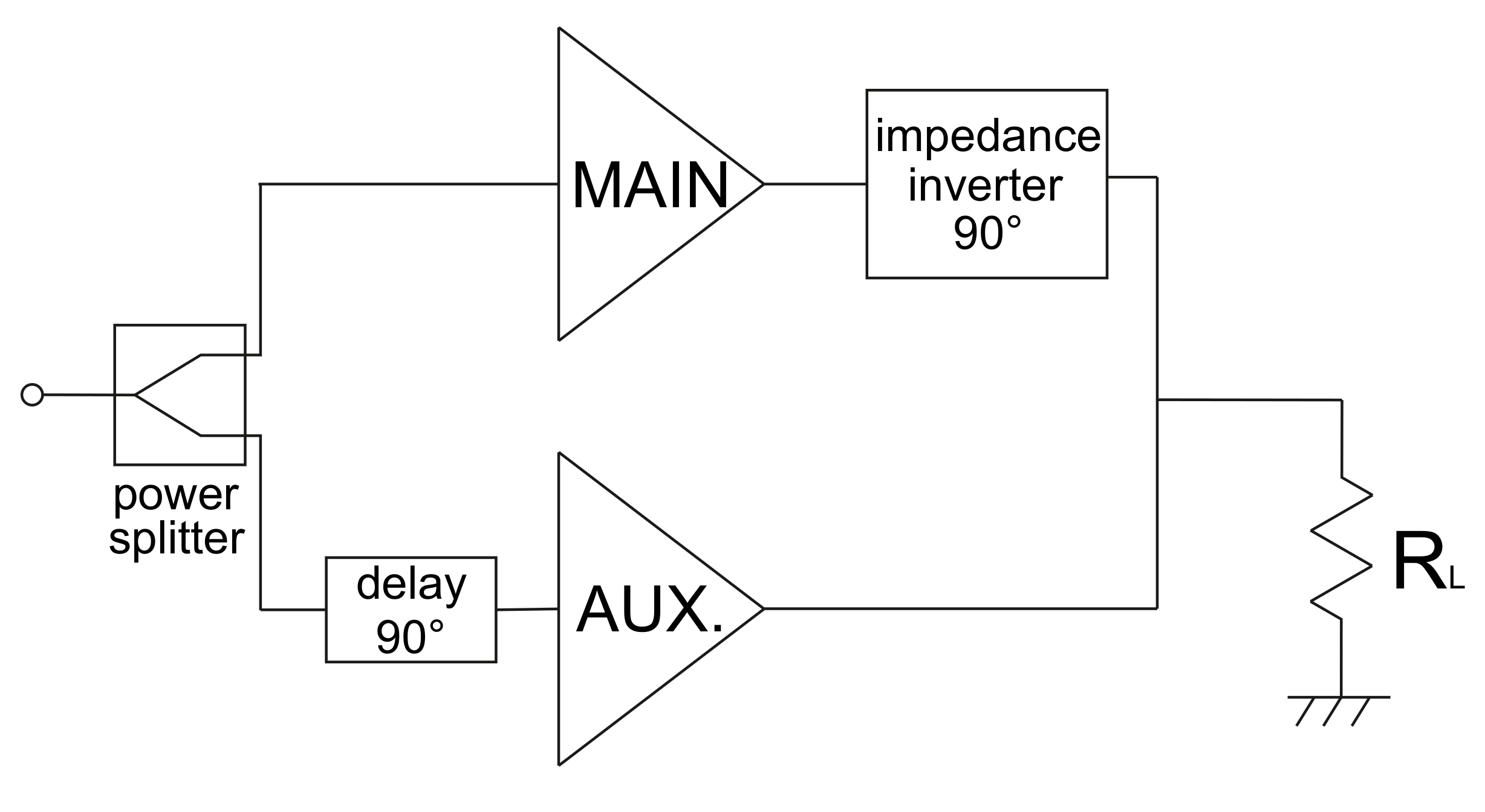
Figure 5.
Simplified equivalent output section of a Doherty Power Amplifier (DPA).
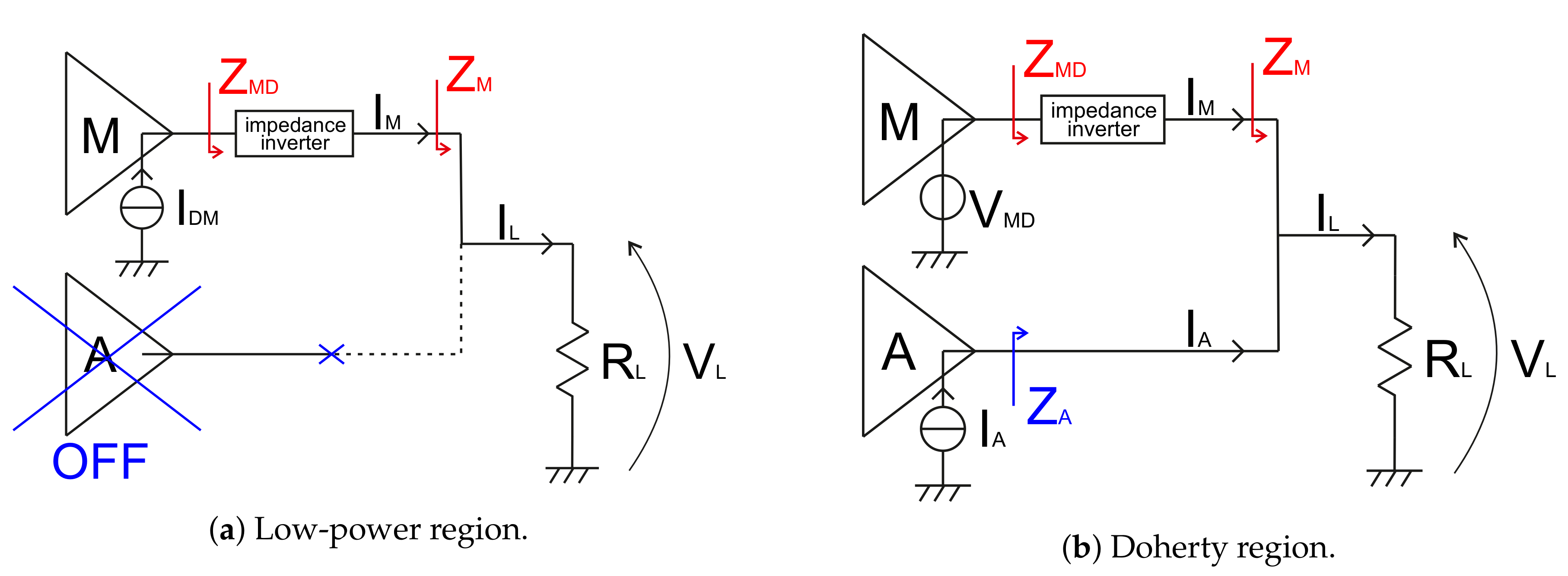
Figure 6.
Doherty power amplifier efficiency. Curves are representative of a Class-AB/C Doherty PA.

Figure 7.
Multi-way and multi-stage DPA efficiencies.

Figure 8.
DPA schematic including matching networks and (red) offset lines.
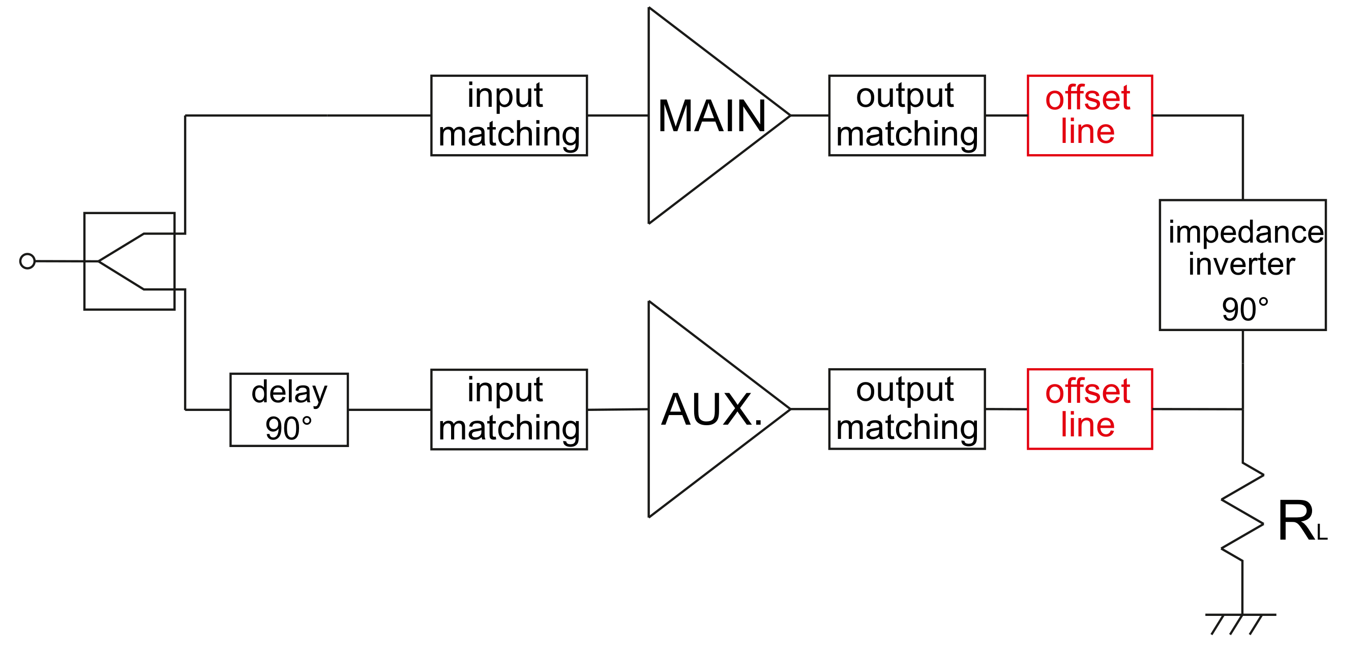
Figure 9.
Digital/dual-input DPA scheme.

Figure 10.
Outphasing power amplifier scheme. SCS: Signal Component Separator; AM: Amplitude-Modulated; PM: Phase-Modulated.
Figure 10.
Outphasing power amplifier scheme. SCS: Signal Component Separator; AM: Amplitude-Modulated; PM: Phase-Modulated.
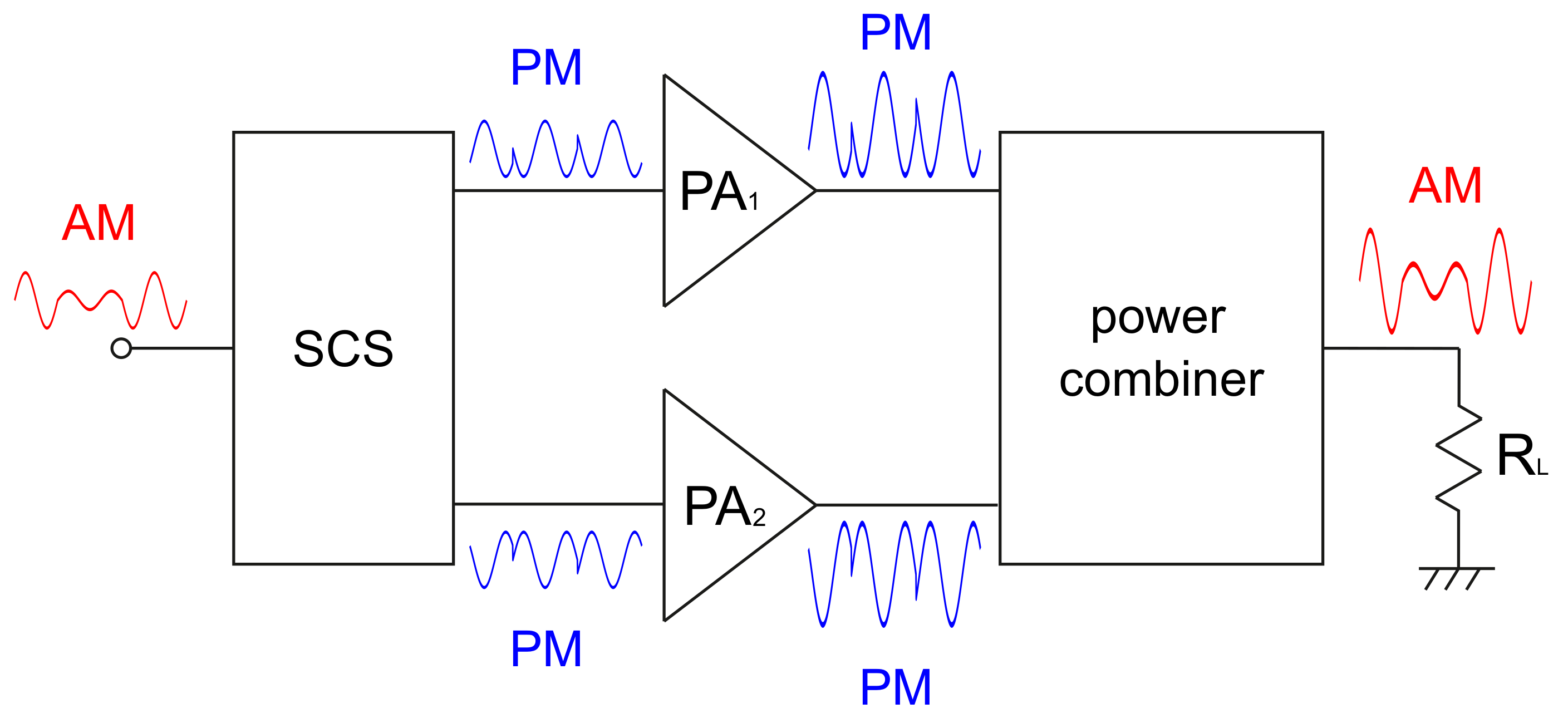
Figure 11.
Simplified output section of an ideal Chireix outphasing amplifier.
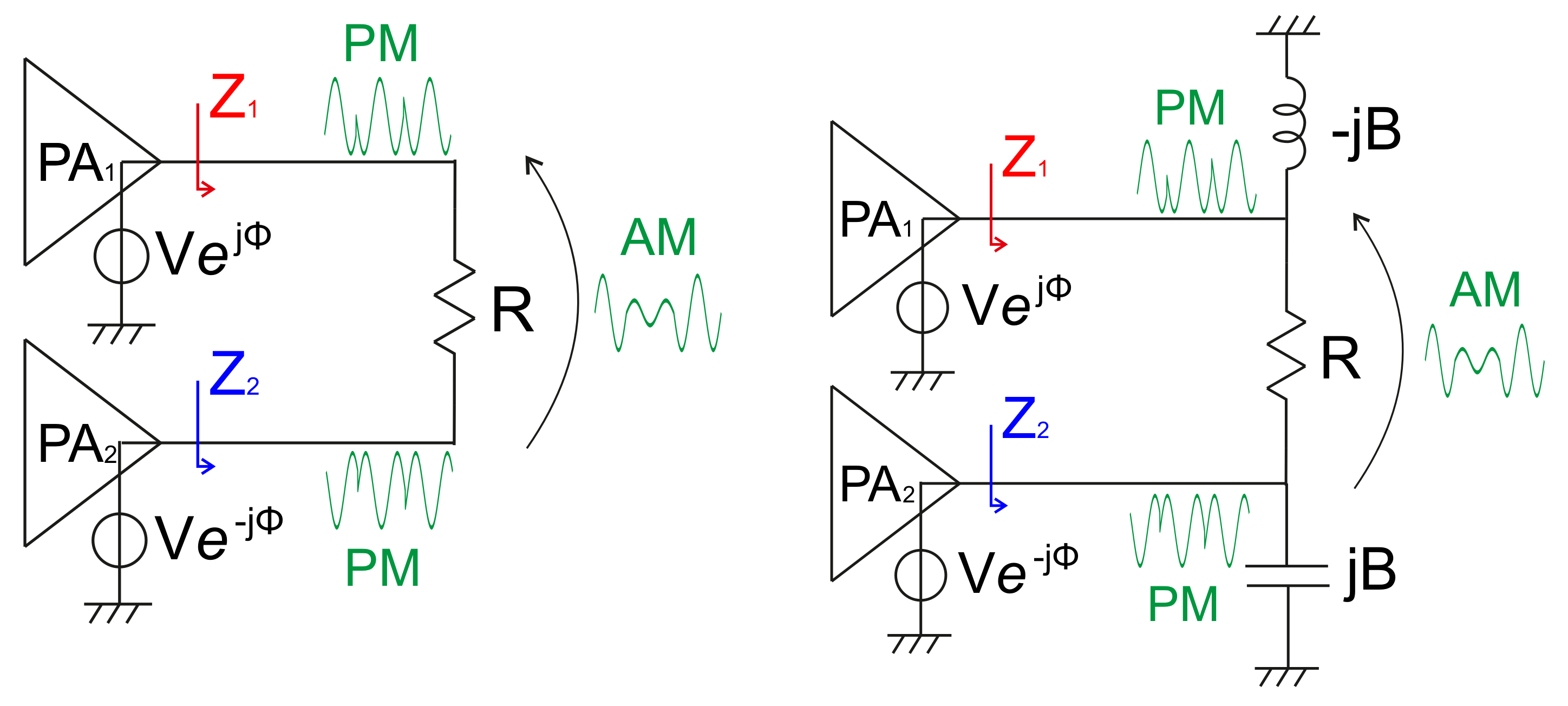
Figure 12.
Load trajectories of the upper (red) and lower (blue) branches for a phase sweep from 0–90.
Figure 12.
Load trajectories of the upper (red) and lower (blue) branches for a phase sweep from 0–90.

Figure 13.
Efficiency vs. OBO curves of Doherty and Chireix amplifiers.
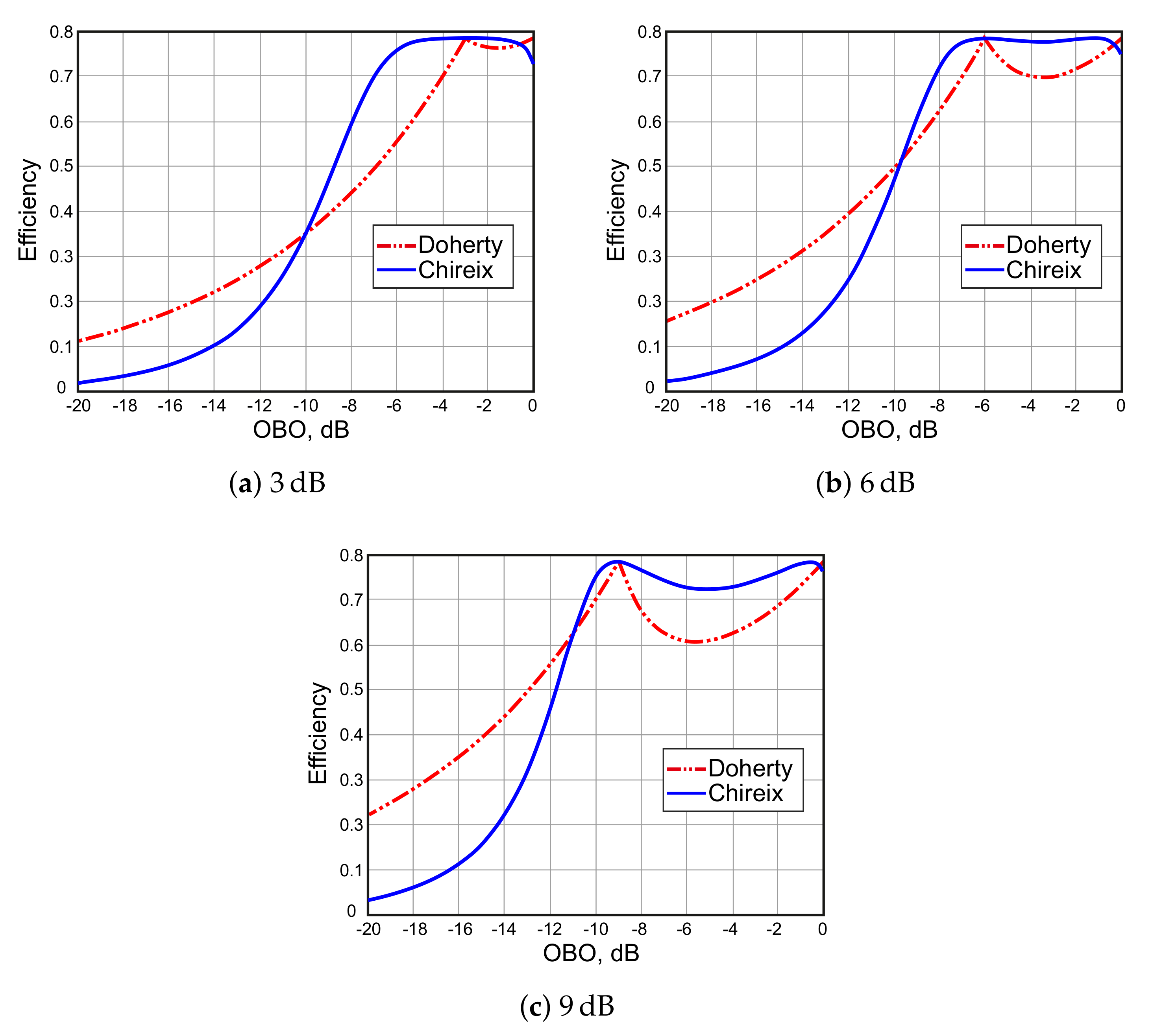
Figure 14.
Typical balun topologies adopted for the Chireix PA output combiner.
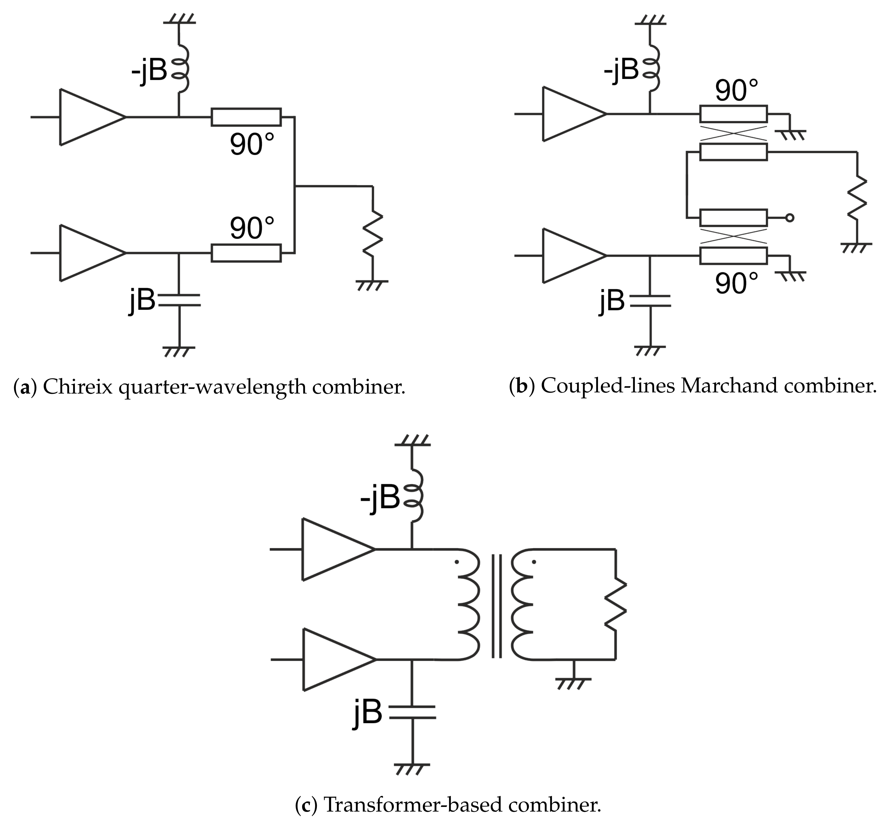
Figure 15.
Conceptual scheme for the realisation of a single-input Chireix PA. AM, Amplitude-Modulated; PM, Phase-Modulated.
Figure 15.
Conceptual scheme for the realisation of a single-input Chireix PA. AM, Amplitude-Modulated; PM, Phase-Modulated.

Figure 16.
Resistance compression network: varies as a function of over a range, set by X, that is only a fraction of the range of variation of .
Figure 16.
Resistance compression network: varies as a function of over a range, set by X, that is only a fraction of the range of variation of .
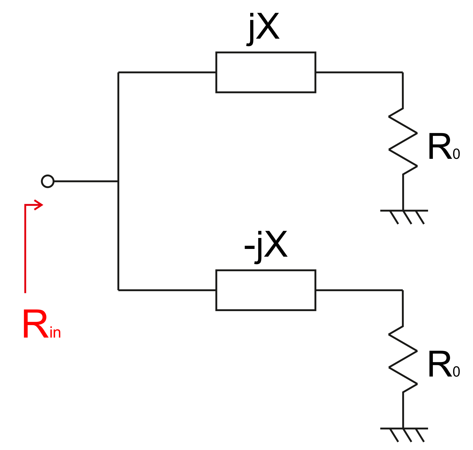
Figure 17.
Dynamic load modulation. RF: Radio Frequency; ENV: Envelope.
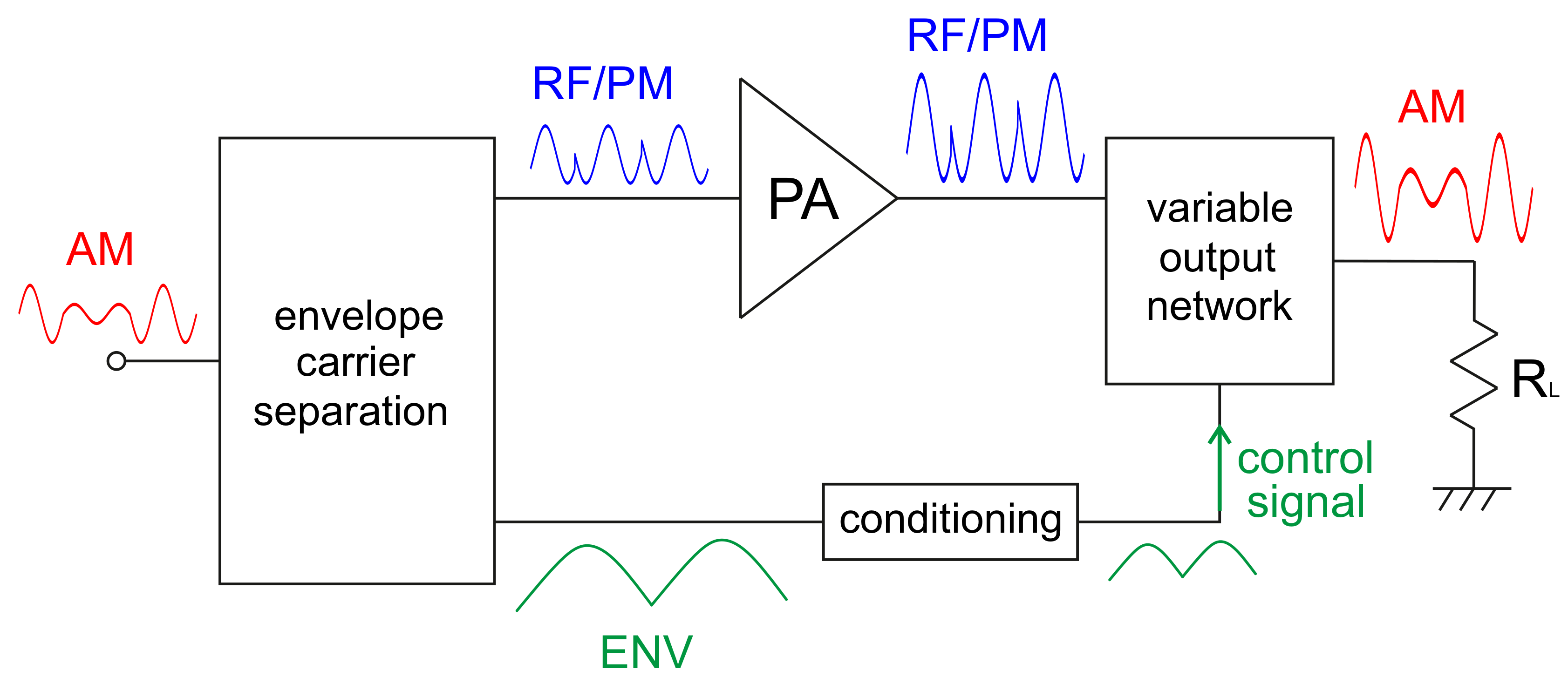
Figure 18.
Discrete Dynamic Load Modulation. PWM: Pulse-Width Modulation.

Figure 19.
Load Modulated Balanced PA (LMBA) scheme.
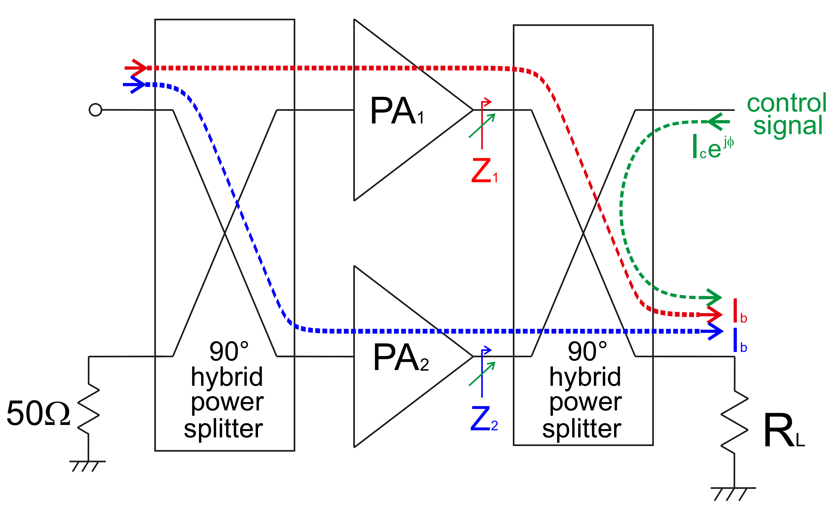
Figure 20.
LMBA impedance modulation curves for different values of .


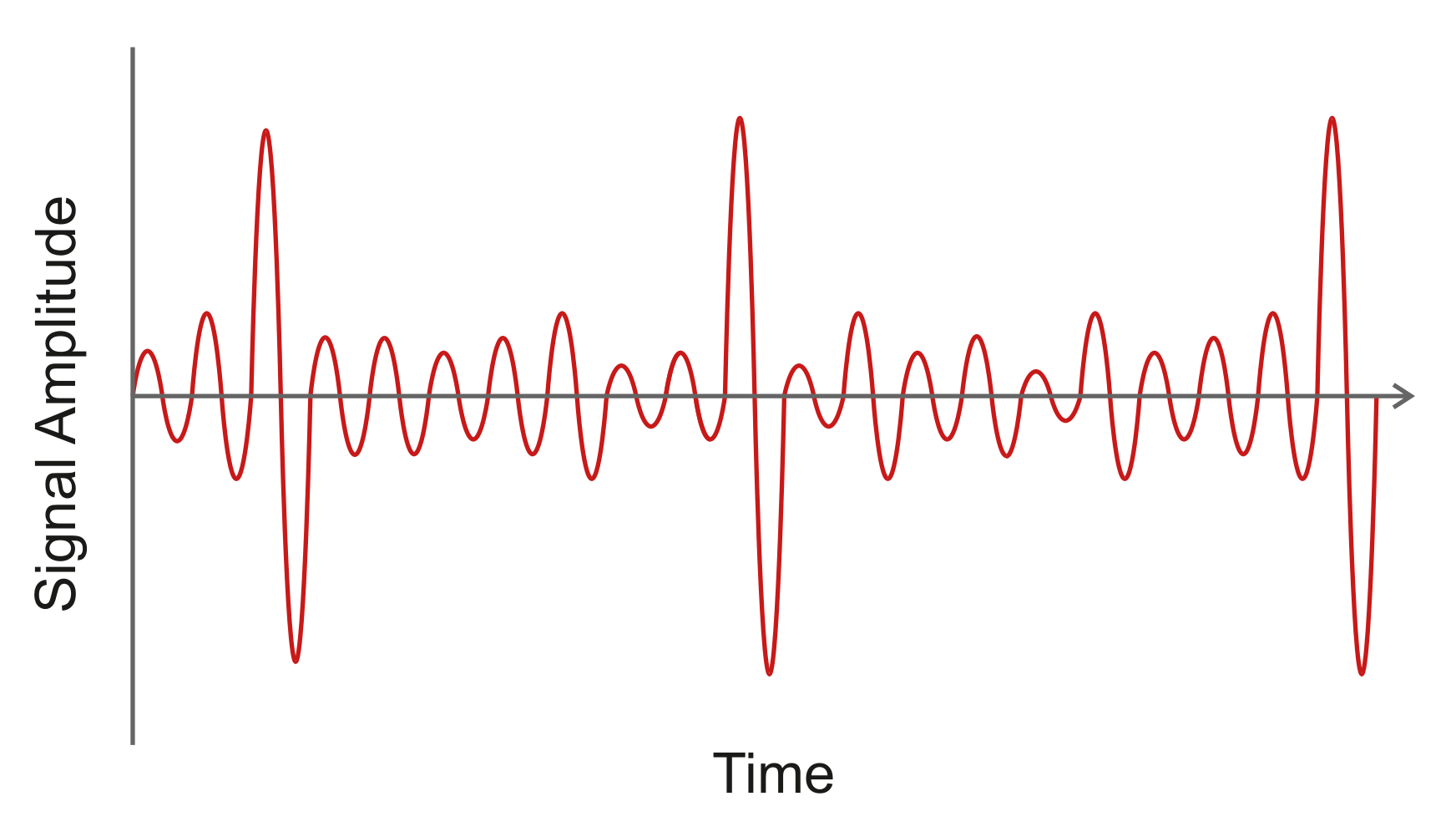
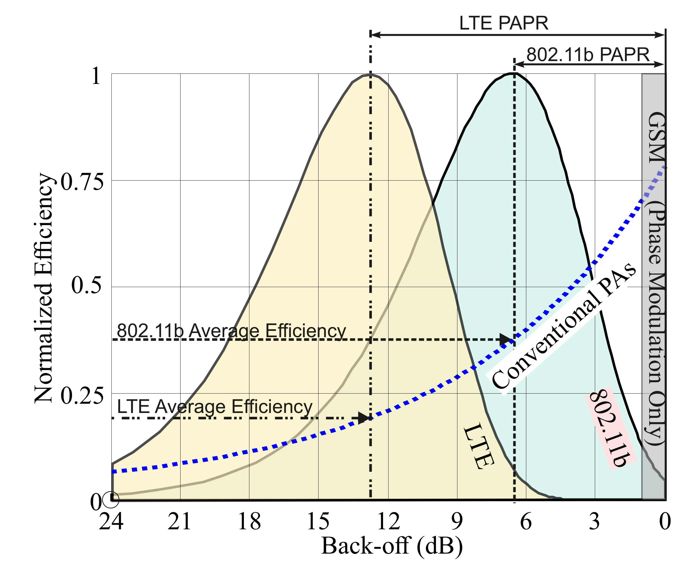
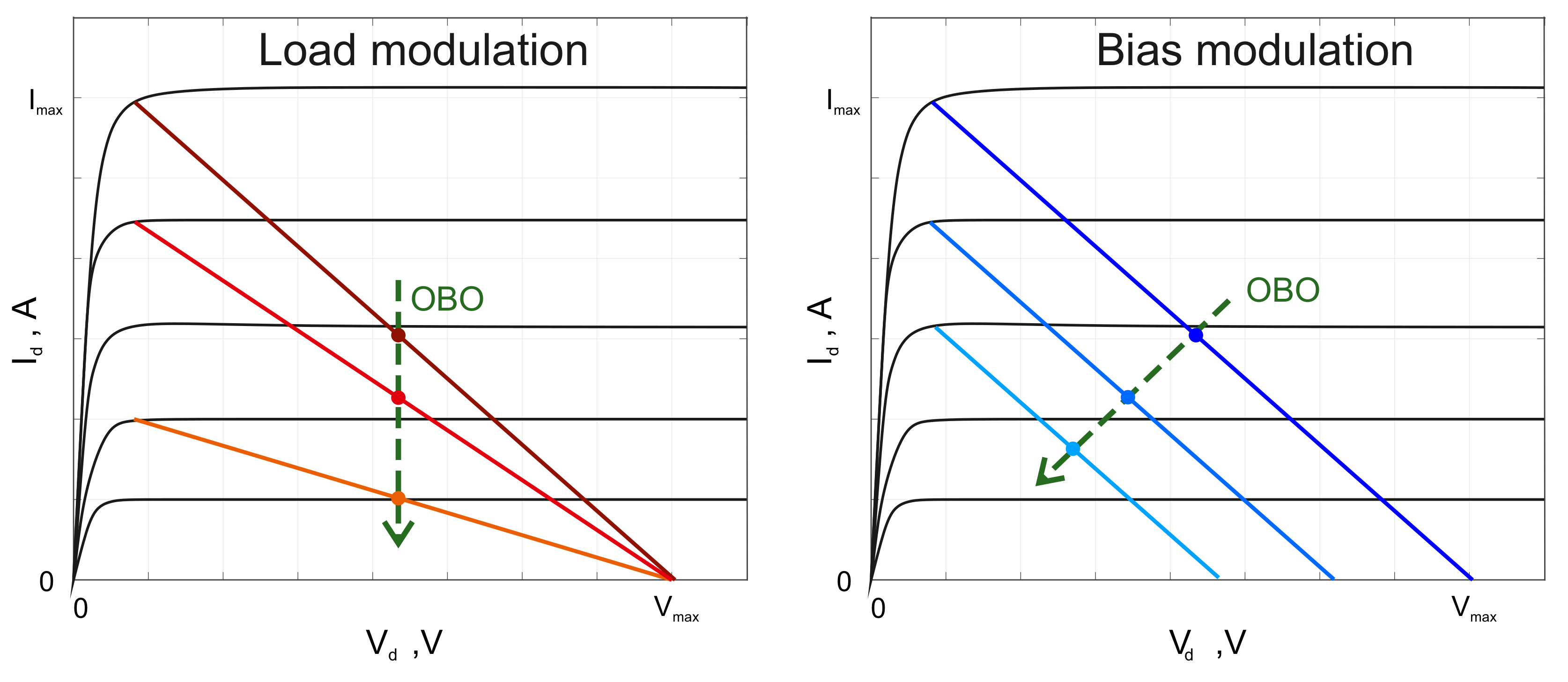
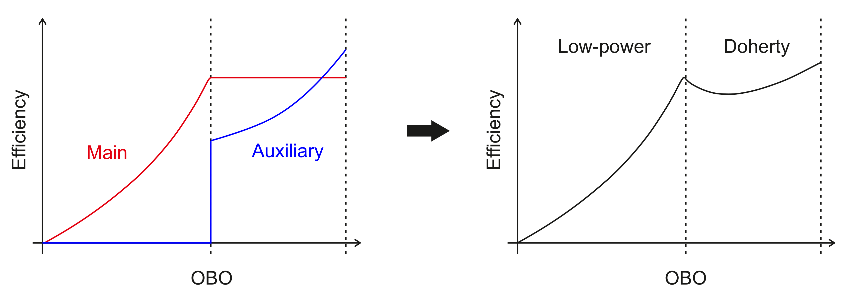
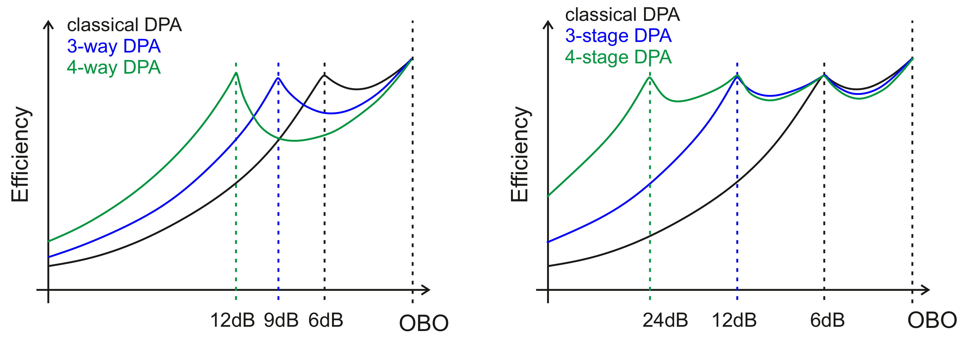
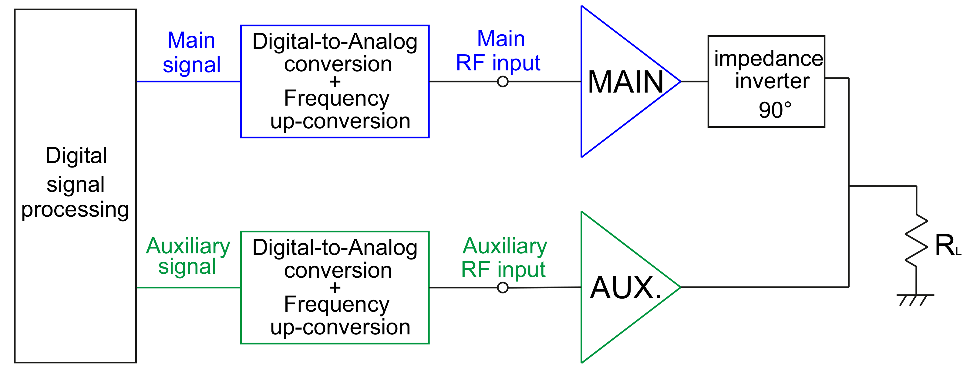
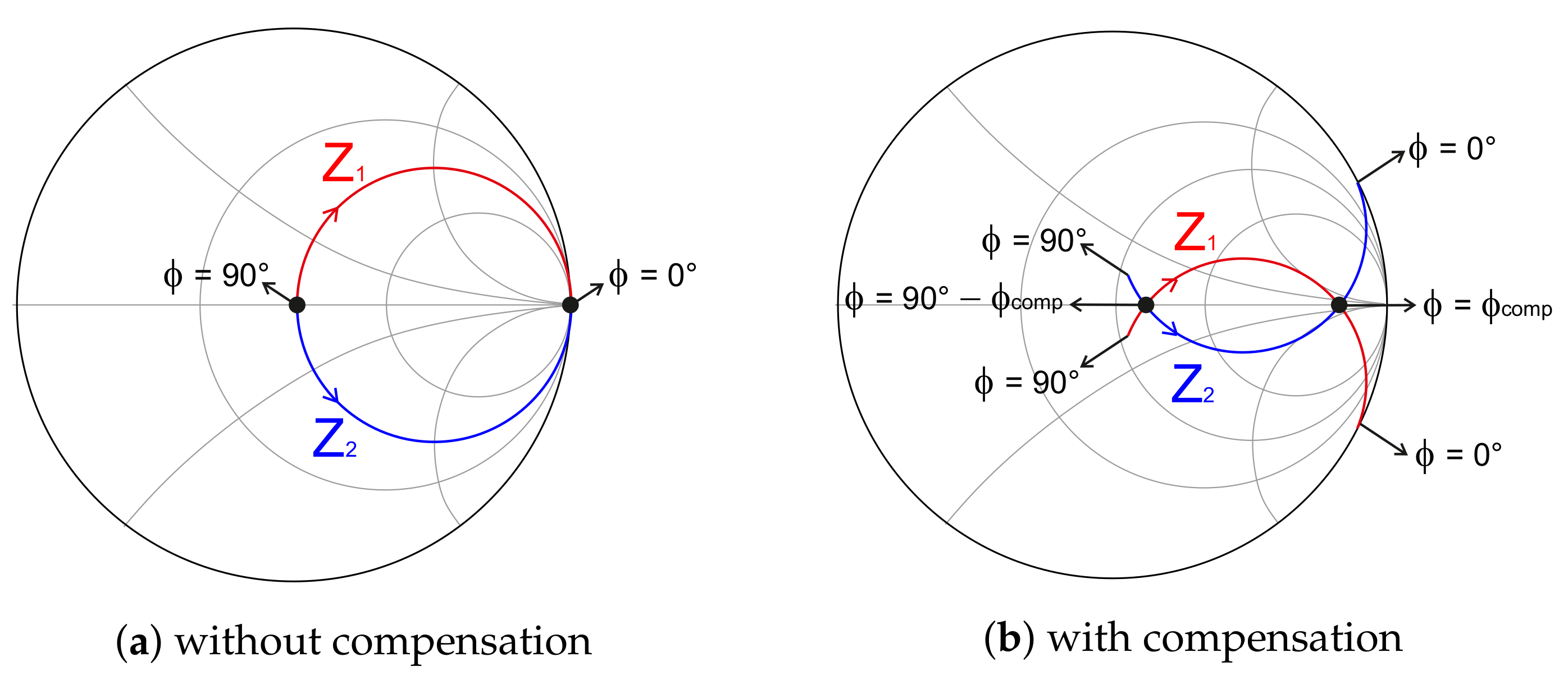
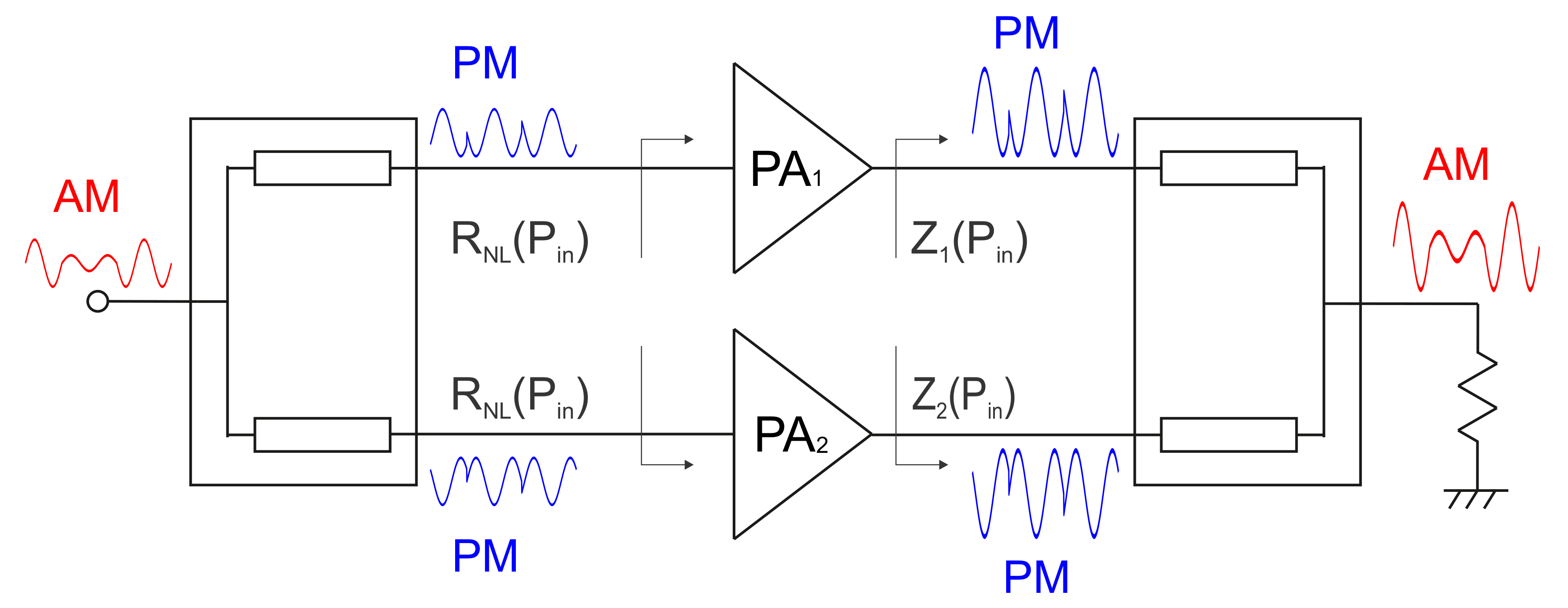
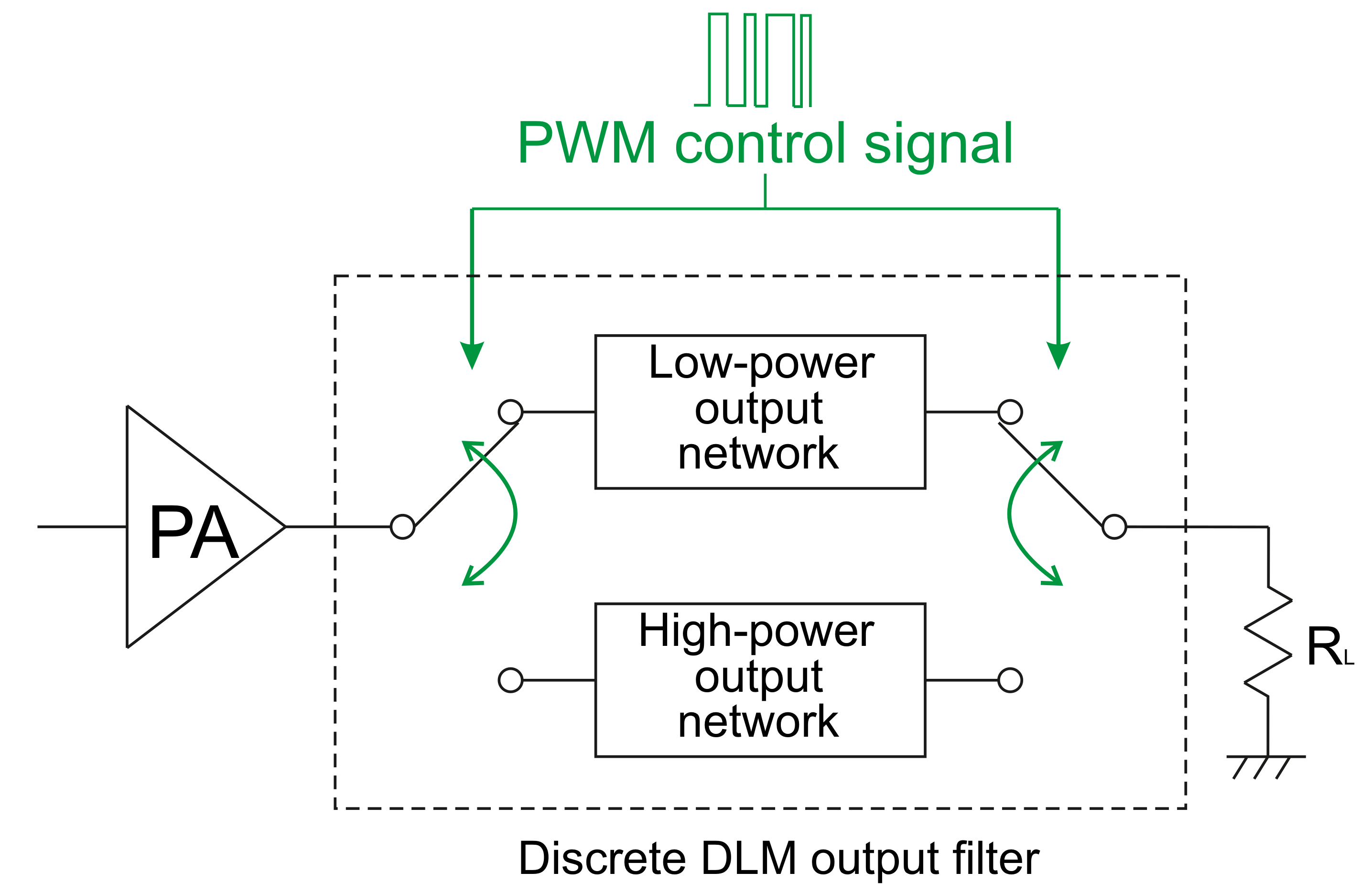
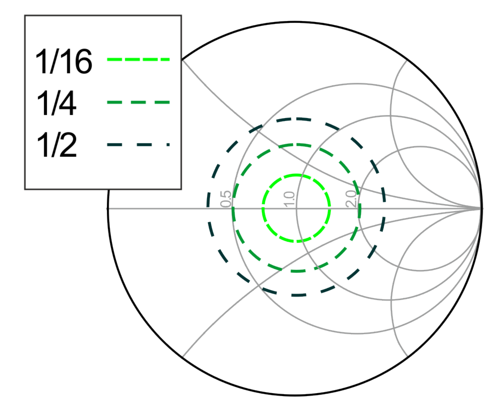
Table 1.
Features of digital mobile communication standards and of microwave backhaul connections.
| Gen. | Standard | Interface and Modulation | Max. Frequency (GHz) | Bandwidth (MH) | Max. Bit-Rate (Mbit/s) | Max. PAPR (dB) |
|---|---|---|---|---|---|---|
| 2G | GSM/EDGE | TDMA/FDMA, GMSK, 8PSK | 1.9 | 0.2 | <1 | 3.3 |
| 3G | UMTS | W-CDMA, QPSK/64QAM | 3 | 5 | 100 | 10.6 |
| 4G | LTE | OFDMA, MIMO 4x4, 64QAM | 5.9 | 20 | 300 | 12 |
| 4G | LTE-Advanced | OFDMA/SC-FDMA, MIMO 8x8, CA, 64QAM | 5.9 | 20 (100 with CA) | >300 | 12 |
| 4G | WiMAX | OFDMA, MIMO 2x2, QPSK/64QAM | 5.8 | 20 | 100 | 12 |
| 5G | 5G | OFDMA, HetNet, massive MIMO, advanced CA, CoMP, … | 40 | >100 (800–2000) | >1000 | >12? |
| 3G/4G backhaul | point-to-point | 4096QAM | 86 GHz | 56 | >800 | 12 |
List of acronyms used in the Table: (Features) PAPR, Peak-to-Average Power Ratio; (Standars) GSM, Global System for Mobile Communications; EDGE, Enhanced Data rates for GSM Evolution; UMTS, Universal Mobile Telecommunications System; LTE, Long-Term Evolution; WiMAX, Worldwide Interoperability for Microwave Access; (Access technology) TDMA, Time-Division Multiple Access; FDMA, Frequency-Division Multiple Access; W-CDMA, Wideband Code-Division Multiple Access; OFDMA, Orthogonal Frequency-division Multiple Access; SC-FDMA, Single-carrier Frequency-Division Multiple Access; (Modulation) GMSK, Gaussian Minimum Shift Keying; PSK, Phase-Shift Keying; QPSK, Quadrature Phase-Shift Keying; QAM, Quadrature Amplitude Modulation; (Interface technology) MIMO, Multiple-Input-Multiple-Output; HetNet, Heterogeneous Networks; CA, Carrier Aggregation; CoMP, Coordinated Multipoint.
© 2017 by the authors. Licensee MDPI, Basel, Switzerland. This article is an open access article distributed under the terms and conditions of the Creative Commons Attribution (CC BY) license (http://creativecommons.org/licenses/by/4.0/).
Share and Cite
MDPI and ACS Style
Ramella, C.; Piacibello, A.; Quaglia, R.; Camarchia, V.; Pirola, M. High Efficiency Power Amplifiers for Modern Mobile Communications: The Load-Modulation Approach. Electronics 2017, 6, 96. https://doi.org/10.3390/electronics6040096
AMA Style
Ramella C, Piacibello A, Quaglia R, Camarchia V, Pirola M. High Efficiency Power Amplifiers for Modern Mobile Communications: The Load-Modulation Approach. Electronics. 2017; 6(4):96. https://doi.org/10.3390/electronics6040096
Chicago/Turabian StyleRamella, Chiara, Anna Piacibello, Roberto Quaglia, Vittorio Camarchia, and Marco Pirola. 2017. "High Efficiency Power Amplifiers for Modern Mobile Communications: The Load-Modulation Approach" Electronics 6, no. 4: 96. https://doi.org/10.3390/electronics6040096
Note that from the first issue of 2016, this journal uses article numbers instead of page numbers. See further details here.