A Compact In-Line Waveguide-to-Microstrip Transition in the Q-Band for Radio Astronomy Applications

 , , ,
, , ,
Abstract
:1. Introduction
2. Design
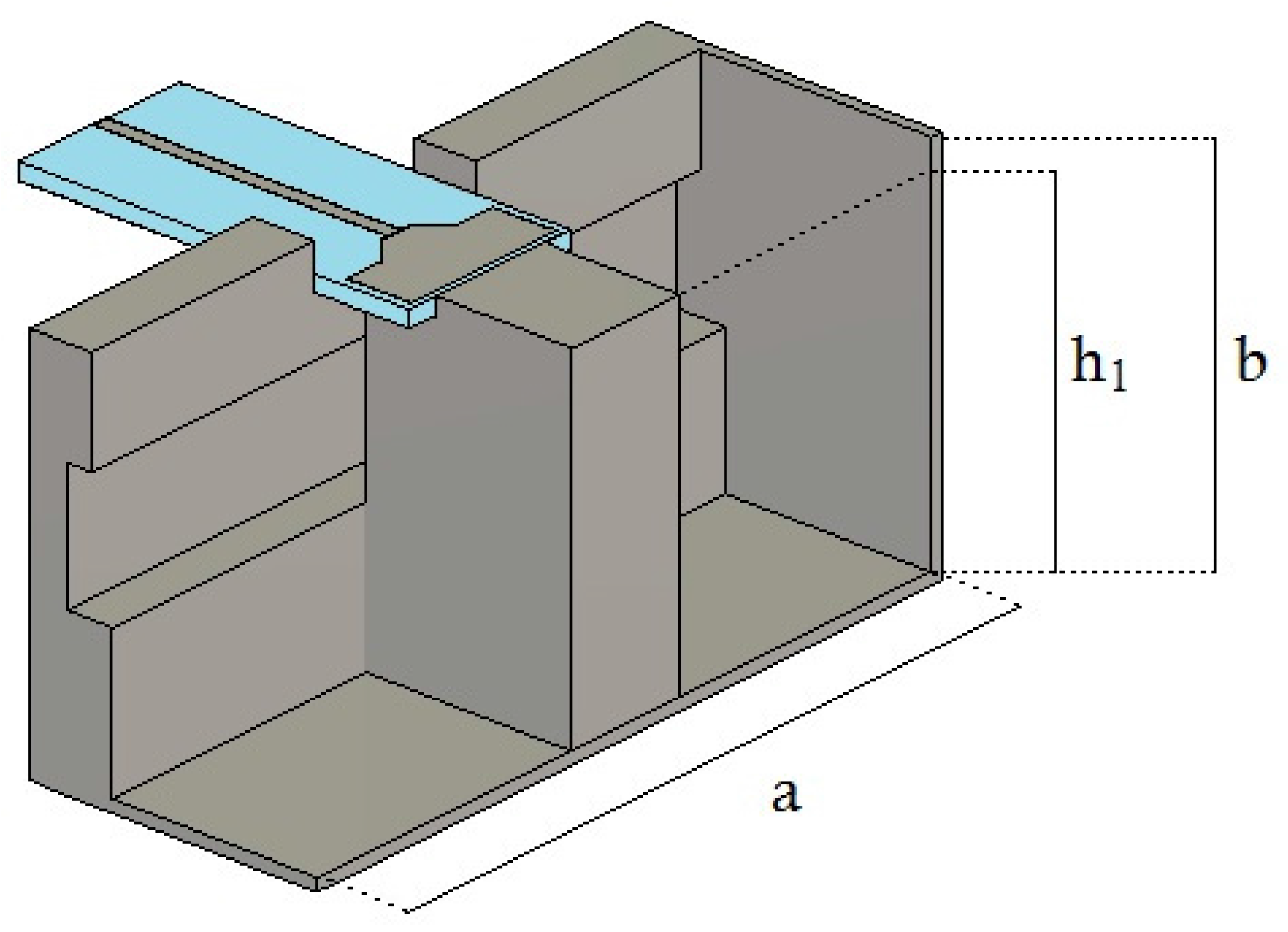
2.1. Theoretical Model
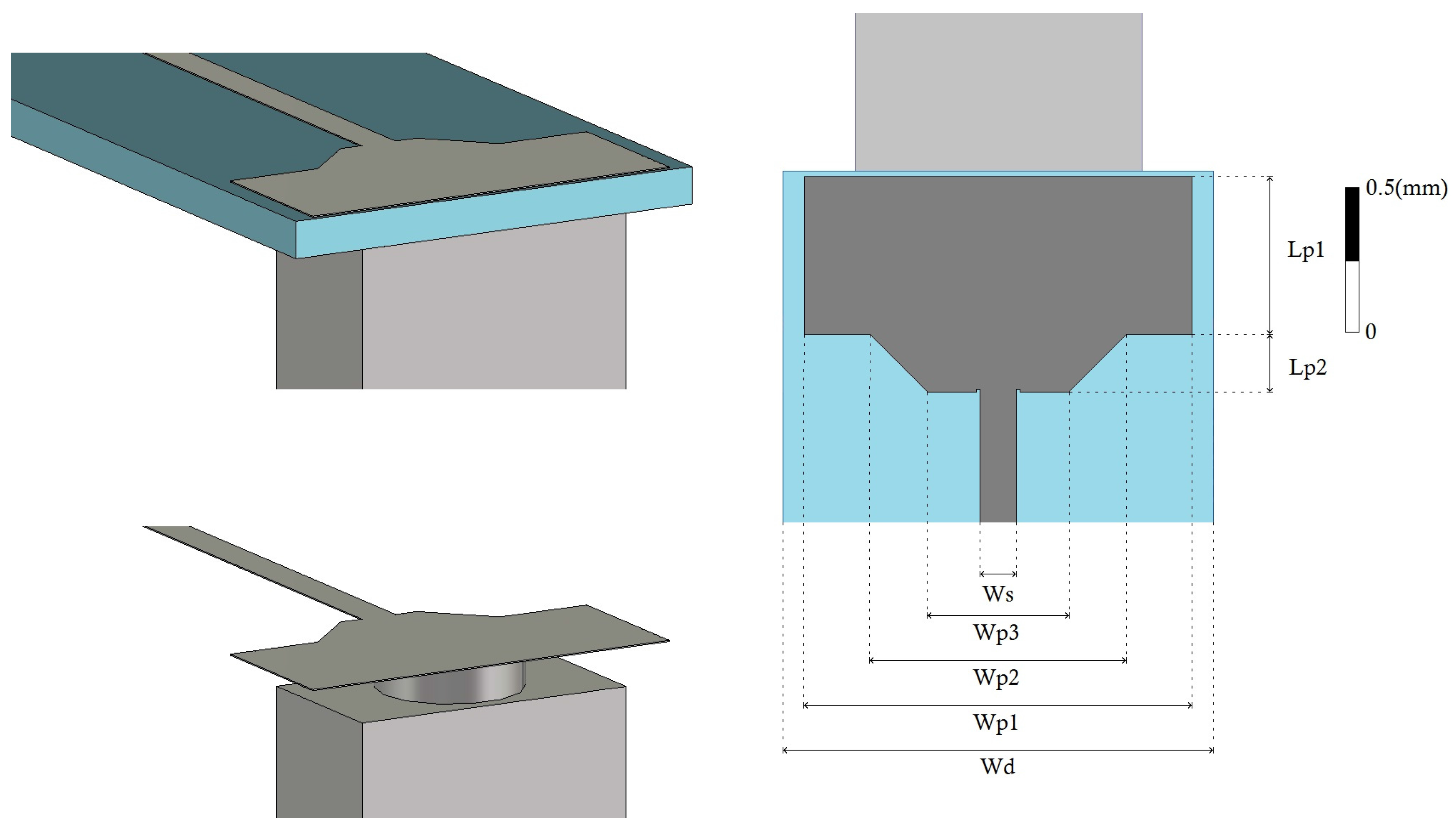
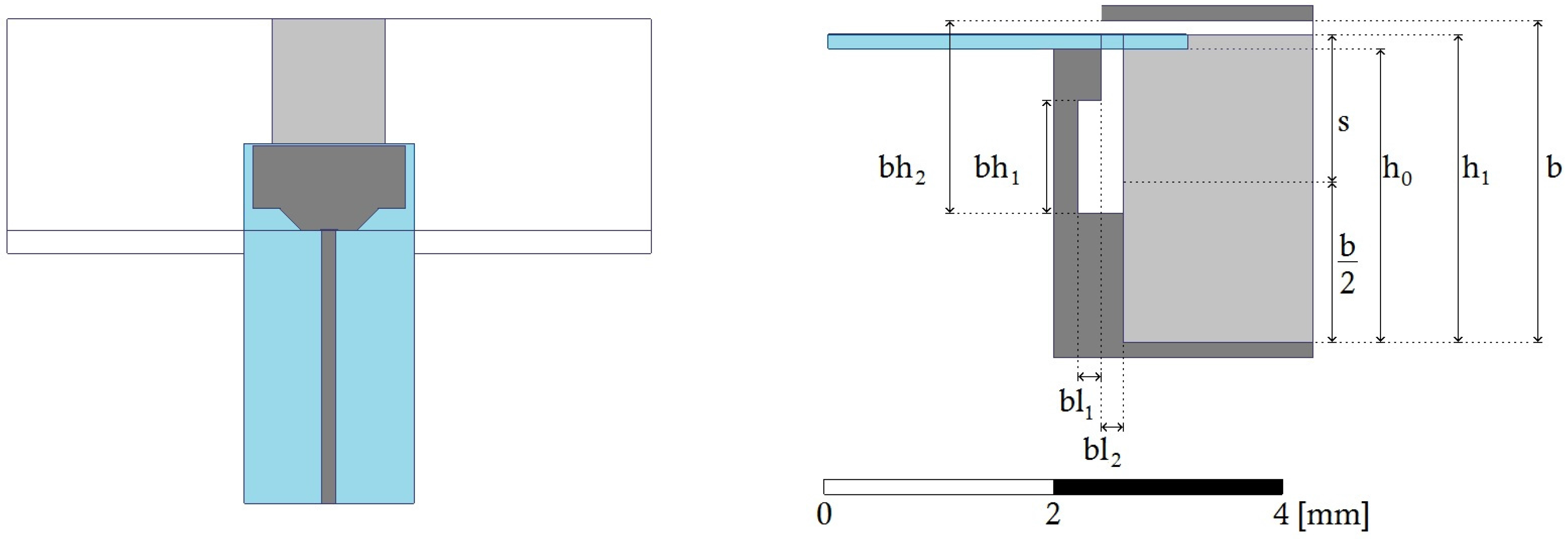
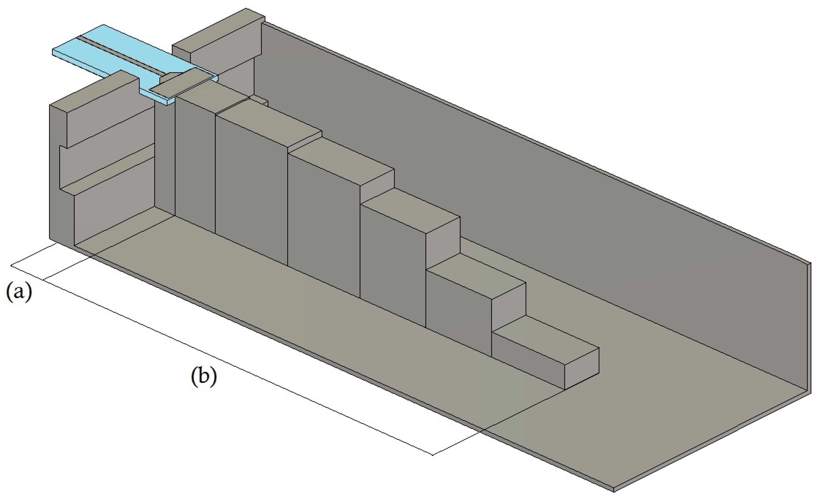
2.2. Design
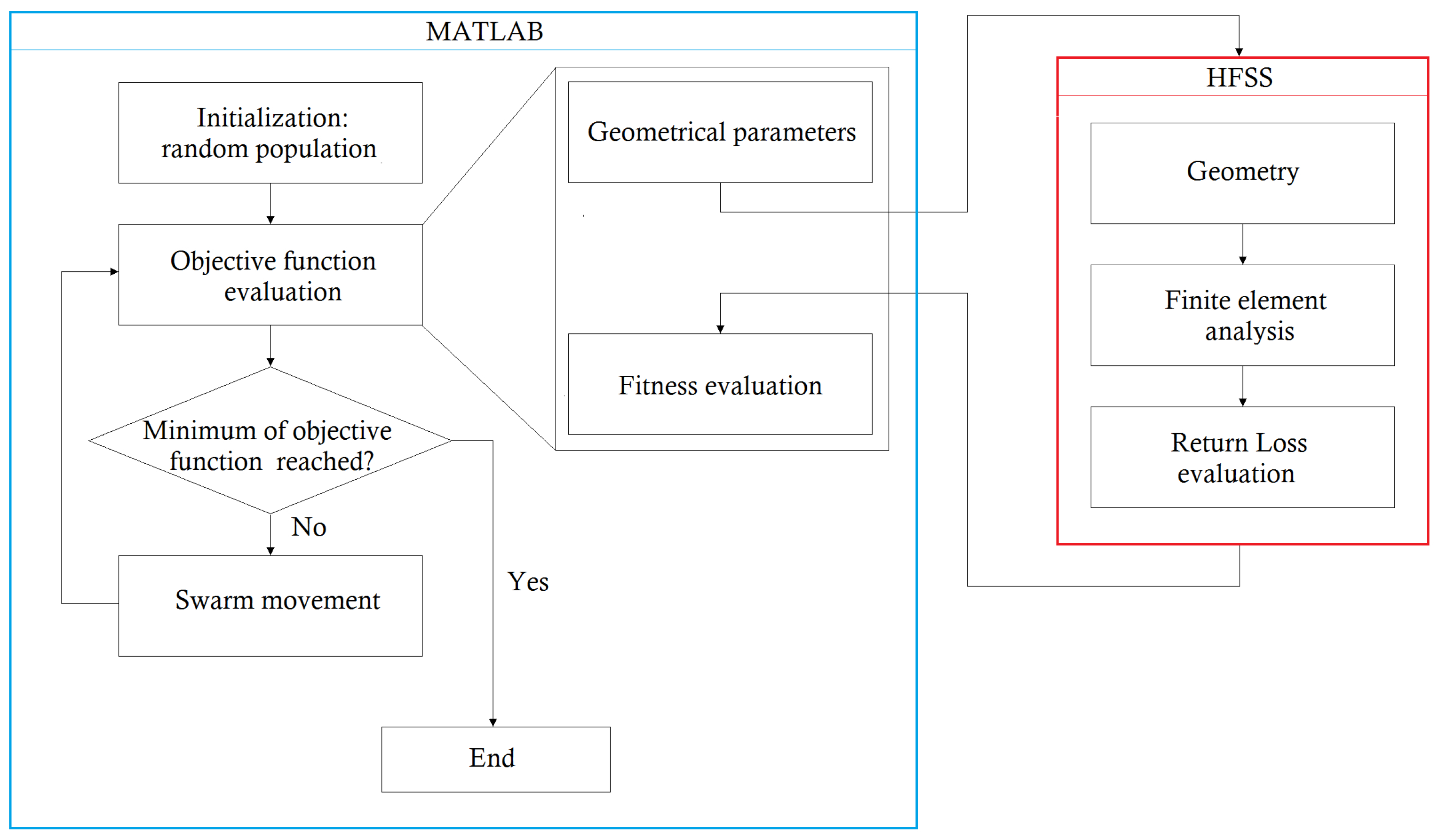
2.3. Optimization
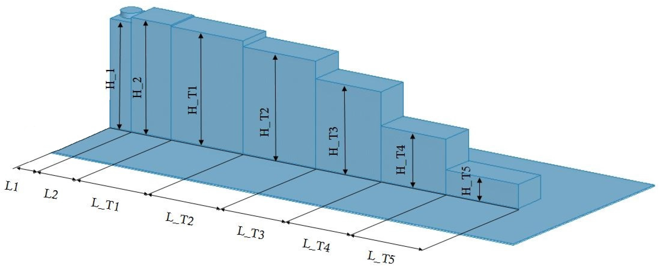
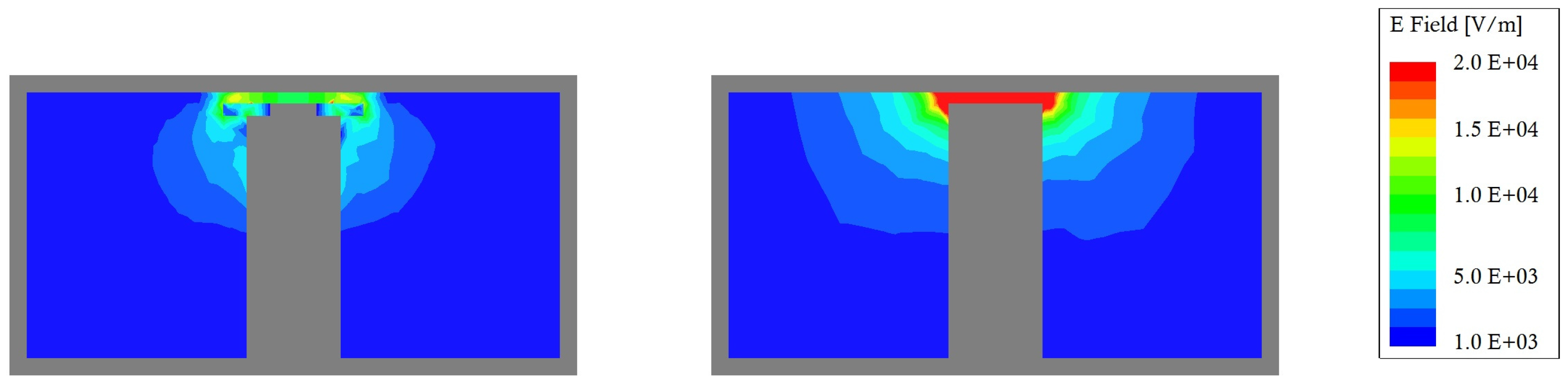
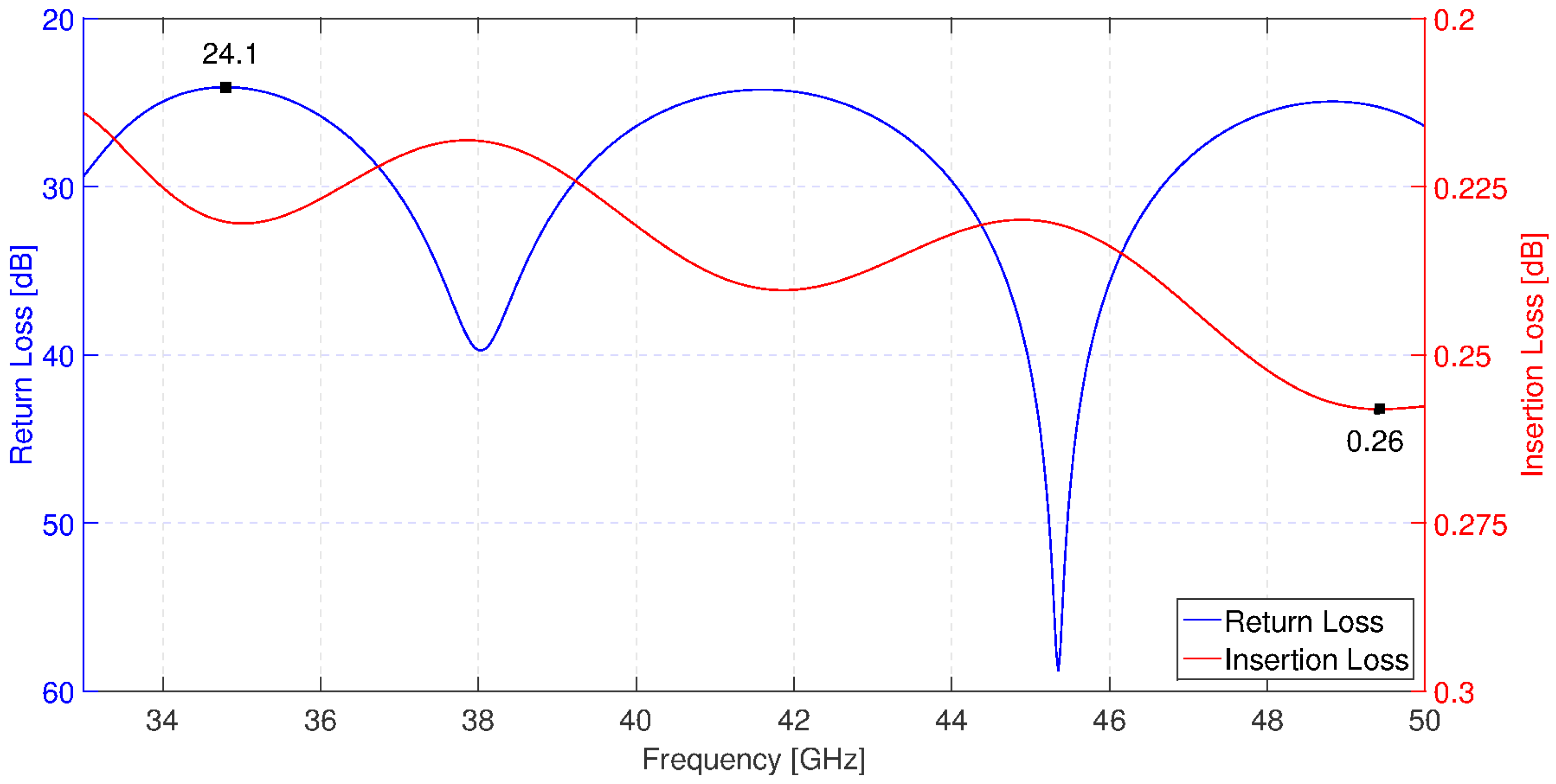
3. Results
4. Conclusions
Author Contributions
Conflicts of Interest
References
- Yeomas, M.E. Radar Receivers. In Radar Handbook; Skolnik, M.I., Ed.; McGraw Hill: New York, NY, USA, 2008. [Google Scholar]
- Kraus, J.D. Radio Astronomy Fundamentals. In Radio Astronomy, 2nd ed.; Cygnus-Quasar Books: Powell, OH, USA, 1986; pp. 101–104. [Google Scholar]
- Valente, G.; Montisci, G.; Pisanu, T.; Navarrini, A.; Marongiu, P.; Casula, G.A. A Compact L-Band Orthomode Transducer for Radio Astronomical Receivers at Cryogenic Temperature. IEEE Trans. Microw. Theory Tech. 2015, 63, 3218–3227. [Google Scholar] [CrossRef]
- Orfei, A.; Carbonaro, L.; Cattani, A.; Cremonini, A.; Cresci, L.; Fiocchi, F.; Maccaferri, A.; Maccaferri, G.; Mariotti, S.; Monari, J.; et al. A Multi-Feed Receiver in the 18 to 26.5 GHz Band for Radio Astronomy. IEEE Antennas Propag. Mag. 2010, 52, 62–72. [Google Scholar] [CrossRef]
- Ladu, A.; Valente, G.; Montisci, G.; Mazzarella, G. A wideband quadruple-ridged horn antenna for the multifeed S-band receiver of the Sardinia Radio Telescope. J. Electromagn. Waves Appl. 2016, 30, 1207–1216. [Google Scholar] [CrossRef]
- Wheeler, G. Broadband waveguide-to-coax transitions. In Proceedings of the 1958 IRE International Convention Record, New York, NY, USA, 21–25 March 1966; Volume 5, pp. 182–185. [Google Scholar]
- Yao, H.-W.; Abdelmonem, A.; Liang, J.-F.; Zaki, K.A. Analysis and design of Microstrip-to-Waveguide Transitions. IEEE Trans. Microw. Theory Tech. 1994, 42, 2371–2380. [Google Scholar]
- Deslandes, D.; Wu, K. Integrated Microstrip and Rectangular Waveguide in Planar Form. IEEE Microw. Wirel. Comp. Lett. 2001, 11, 68–70. [Google Scholar] [CrossRef]
- Simeoni, M.; Coman, C.I.; Lager, I.E. Patch End-Launchers—A Family of Compact Colinear Coaxial-to-Rectangular Waveguide Transitions. IEEE Trans. Microw. Theory Tech. 2006, 54, 2371–2380. [Google Scholar] [CrossRef]
- Kaneda, N.; Qian, Y.; Itoh, T. A Broad-Band Microstrip-to-Waveguide Transition Using Quasi-Yagi Antenna. IEEE Trans. Microw. Theory Tech. 1999, 47, 2562–2567. [Google Scholar] [CrossRef]
- Fang, R.-Y.; Wang, C.-L. Miniaturized Microstrip-to-Waveguide Transition Using Capacitance-Compensated Broadside-Coupled Microstrip Line. IEEE Trans. Comp. Packag. Manuf. Technol. 2013, 3, 1588–1596. [Google Scholar] [CrossRef]
- Jing, S.; Fa-guo, L.; Li-hua, H.; Xiao-ying, S.; Yan-qiu, Z. Waveguide-to-Microstrip Antipodal Finline Transition at W Band. In Proceedings of the 2013 Third International Conference on Instrumentation, Measurement, Computer, Communication and Control, Shenyang, China, 21–23 September 2013; pp. 510–513. [Google Scholar]
- Rebollo, A.; Larumbe-Gonzalo, B.; Gonzalo, R.; Ederra, I. Full W-Band Microstrip-to-Waveguide Inline Transition. In Proceedings of the 8th European Conference on Antennas and Propagation (EuCAP 2014), The Hague, The Netherlands, 6–11 April 2014; pp. 2591–2593. [Google Scholar]
- Han, K.Y.; Pao, C.-K. A V-band waveguide to microstrip inline transition. In Proceedings of the 2012 IEEE/MTT-S International Microwave Symposium Digest, Montreal, QC, Canada, 17–22 June 2012. [Google Scholar]
- Collin, R.E. Theory and Design of Wide-Band Multisection Quarter-Wave Transformers. Proc. IRE 1955, 43, 179–185. [Google Scholar] [CrossRef]
- Pozar, D.M. Impedance Matching and Tuning. In Microwave Engineering; Pozar, D.M., Ed.; John Wiley & Sons, Inc.: Hoboken, NJ, USA, 2011; pp. 256–261. [Google Scholar]
- Helszajn, J.; Caplin, M. Impedance and propagation in ridge waveguides using the transverse resonance method. In Ridge Waveguides and Passive Microwave Components; Helszajn, J., Ed.; IET Electromagnetic Waves Series; The Institution of Engineering and Technology: London, UK, 2000; pp. 46–49. [Google Scholar]
- Simone, M.; Fanti, A.; Mazzarella, G. Ridge waveguide optimization with PSO algorithm. J. Electromagn. Waves Appl. 2015, 29, 199–209. [Google Scholar] [CrossRef]
- Simone, M.; Fanti, A.; Montisci, G.; Casula, G.A.; Mazzarella, G. Combined PSO-FDFD Optimization of Rectangular Ridged Waveguides. ACES J. 2016, 31, 144–151. [Google Scholar]
- Casula, G.A.; Mazzarella, G.; Montisci, G. Design of Shaped Beam Planar Arrays of Waveguide Longitudinal Slots. Int. J. Antennas Propag. 2013. [Google Scholar] [CrossRef]
- Yang, H.; Jin, Z.; Montisci, G.; Liu, Y.; He, X.; Casula, G.A.; Mazzarella, G. Design Equations for Cylindrically Conformal Arrays of Longitudinal Slots. IEEE Trans. Antennas Propag. 2016, 64, 80–88. [Google Scholar] [CrossRef]
- Tekkouk, K.; Hirokawa, J.; Sauleau, R.; Ando, M. Wideband and Large Coverage Continuous Beam Steering Antenna in the 60-GHz Band. IEEE Trans. Antennas Propag. 2017, 65, 4418–4426. [Google Scholar] [CrossRef]
- Hsu, S.; Wei, K.-C.; Hsu, C.-Y.; Ru-Chuang, H. A 60-GHz Millimeter-Wave CPW-Fed Yagi Antenna Fabricated by Using 0.18-μm CMOS Technology. IEEE Electron Device Lett. 2008, 29, 625–627. [Google Scholar]
- Mikulasek, T.; Lacik, J.; Puskely, J.; Raida, Z. Design of aperture-coupled microstrip patch antenna array fed by SIW for 60 GHz band. IET Microw. Antennas Propag. 2016, 10, 288–292. [Google Scholar] [CrossRef]


| Height | [mm] | Length | [mm] |
|---|---|---|---|
| H_1 | 2.6 | L_1 | 0.57 |
| H_2 | 2.72 | L_2 | 1.1 |
| H_T1 | 2.69 | L_T1 | 2 |
| H_T2 | 2.55 | L_T2 | 2 |
| H_T3 | 2.13 | L_T3 | 1.81 |
| H_T4 | 1.31 | L_T4 | 1.81 |
| H_T5 | 0.57 | L_T5 | 2 |
© 2018 by the authors. Licensee MDPI, Basel, Switzerland. This article is an open access article distributed under the terms and conditions of the Creative Commons Attribution (CC BY) license (http://creativecommons.org/licenses/by/4.0/).
Share and Cite
Simone, M.; Fanti, A.; Valente, G.; Montisci, G.; Ghiani, R.; Mazzarella, G. A Compact In-Line Waveguide-to-Microstrip Transition in the Q-Band for Radio Astronomy Applications. Electronics 2018, 7, 24. https://doi.org/10.3390/electronics7020024
Simone M, Fanti A, Valente G, Montisci G, Ghiani R, Mazzarella G. A Compact In-Line Waveguide-to-Microstrip Transition in the Q-Band for Radio Astronomy Applications. Electronics. 2018; 7(2):24. https://doi.org/10.3390/electronics7020024
Chicago/Turabian StyleSimone, Marco, Alessandro Fanti, Giuseppe Valente, Giorgio Montisci, Riccardo Ghiani, and Giuseppe Mazzarella. 2018. "A Compact In-Line Waveguide-to-Microstrip Transition in the Q-Band for Radio Astronomy Applications" Electronics 7, no. 2: 24. https://doi.org/10.3390/electronics7020024