Power Efficient Fully Differential Bulk Driven OTA for Portable Biomedical Application


Electronic Engineering Department, NED University of Engineering and Technology, Karachi 75270, Pakistan
*
Author to whom correspondence should be addressed.
Electronics 2018, 7(3), 41; https://doi.org/10.3390/electronics7030041
Submission received: 19 February 2018
/
Revised: 13 March 2018
/
Accepted: 16 March 2018
/
Published: 20 March 2018
Abstract
:This paper presents a power efficient, bulk driven, source degenerated fully differential operational transconductance amplifier (OTA), operating in the subthreshold region. The input part of the OTA consists of a bulk driven source degenerated differential pair and cross coupled transistors to improve the linearity of OTA. It consists of a bulk driven pair to reduce the supply voltage and to improve the linearity. The proposed fully differential OTA has utilized self-cascode current mirror loads which increases the output impedance and hence the overall intrinsic gain. A subthreshold region is adopted to reduce the power consumption of the circuit. For a 200 mVpp sinusoidal input at 100 Hz, a total harmonic distortion (THD) of −58.56 dB is achieved. The gain, gain bandwidth (GBW), phase margin (PM) and gain margin (GM) values obtained were 48.4 dB, 3.1 KHz, 80° and 19.01 dB, respectively. The common mode rejection ratio (CMRR), power supply rejection ratio (PSRR) and slew rate +/− values were 146.3 dB, 83 dB and 99.56/100 V/ms, respectively. The circuit is capable of operating under a supply voltage of 0.8 V with a power consumption of 59.04 nW, which proves that the circuit is suitable for portable biomedical devices. The proposed circuit is simulated in CADENCE environment virtuoso using LFoundry 150 nm Complementary metal oxide semiconductor (CMOS) process technology.
1. Introduction
With the increasing demand for portable battery operated biomedical devices, there is a growing need for the development of new design techniques for low voltage (LV), low power (LP), integrated circuits (IC) [1]. The biomedical field is rapidly changing and moving towards portability; thus, low power consumption is highly desirable for devices which monitor patients throughout the day [2]. Biomedical devices should be portable and durable due to the constraints of avoiding frequent replacement of batteries and having power efficient circuits as well as low supply voltages so that these devices can be used for a prolonged period of time [3]. Keeping the size and weight of the devices as small as possible without affecting the quality is extremely important; therefore, it is desirable to use as few batteries as possible, which demands low voltage operations [4]. Low voltage operation is also demanded because there is a continued down-scaling of processes. As the channel length of the metal oxide semiconductor (MOS) transistor is scaled down, the gate-oxide thickness becomes only several nanometers thick, and the supply voltage has to be reduced in order to ensure device function and reliability. Nowadays, the allowable supply voltage has gone below 1 V [5]. Not only this, there is an increasing density of components on the chip, and a silicon chip can only have a limited amount of power per unit area. Since the increasing density of components allows for more electronic functions per unit area, the power per electronic function has to be lowered in order to prevent overheating of the chip; thus LV LP designs are necessary [6]. Different design techniques have been proposed in the literature to reduce the supply voltage as well as the power consumption [7,8,9], but the reduction in the threshold voltage (Vth) has not been reduced by the same amount. With a low supply voltage, the threshold voltage is the main limitation in designing of low voltage analog integrated circuits [10]. This issue has been resolved by using the low threshold voltage MOS-like flipped voltage flower [11], the floating gate [12], the pseudo differential approach [13], the bulk driven MOS [14], the sub-threshold operation [15], etc. Out of these methods, sub-threshold operation is the best choice for low voltage, low power and low frequency biomedical applications. Bulk driven technique is also one promising approach for low voltage operations as it is compatible with the CMOS process and does not require any change in the conventional MOS transistor [16]; this not only allows for a large signal swing, but also a reduced open loop gain and unity gain bandwidth (UGBW) [17]. It is suitable for low voltage operations as it removes the threshold voltage from the signal path, but its bulk source transconductance (gmb) is 3–5 times smaller than the gate source transconductance (gm) [18], and it increases the input referred noise. A low GBW does not matter for biomedical low frequency signals, but its intrinsic gain is reduced [7].
The operational transconductance amplifier (OTA) is one of the most important building blocks used in various applications, such as data converters, oscillators, continuous time filters and analog to digital converters [19]. One drawback of OTA is its limited linear range which has to be increased to reduce the distortion at the output [20]. Bio signals, such as the electrocardiogram (ECG), electroencephalogram (EECG) and electromyogram (EMG) are low power, low voltage signals. Different bio signals have different amplitudes and frequencies ranging from 1 uV to 500 mV with low frequencies up to a few KHz. Various design techniques have been reported in recent years to achieve transconductance in the order of a few nA/V and to enhance the linear range, such as input attenuation [21], source degeneration [22], cross coupled differential pairs [23] and the adaptive biasing technique [24]. Bulk driven MOS transistors were used in [25] to control the cancellation factor, and the transconductance was linearly adjusted by bulk voltage. A feed-forward technique was used in [26] to cancel out the third order nonlinear component of OTA, but its improved performance was achieved at the expense of high noise and increased power. Source degeneration, nonlinear term cancellation and current division technique was used in [27] to improve the linear range up to +/− 0.4 V under a supply voltage of 1 V. The linearity of OTA is an important issue because the overall system performance is determined by the linearity of OTA. This issue becomes challenging when low voltage and low power are the major concerns [28]. The use of complex architecture to enhance the linear range has drawbacks since it increases noise, mismatches and the chip area, which degrades the performance of the circuit. OTA, operated in the subthreshold region, is associated with low voltage, low power circuits, as it favors LV design due to its reduced VDS of about 78 mV, rather than the 200 mV that is required for strong inversion saturation MOS [17]. In the subthreshold region, OTA has a narrow linear range, because in this region, the MOS transistor depends exponentially on the voltage. Source degeneration is the one of the simplest methods used to linearize the OTA; it uses passive resistors to enhance the linearity, but these passive resistors can occupy a large area so can be replaced with an MOS, operated in the triode region. This reduces the distortion component and the transconductance value as well [29].
The objective of this research is to design a power efficient, low voltage circuit, suitable for biomedical application, to avoid frequent battery replacement in portable devices and to allow operation of the device for a prolonged period of time. This work further focuses on improving the linearity of the circuit to reduce the distortion at the output and achieve a high performance OTA circuit. In this paper, a fully differential, bulk driven, source degenerated, differential pair, operating in the weak inversion region is proposed. The bulk driven method is used to reduce the threshold voltage which, in turn, reduces the supply voltage. Weak inversion is adopted to reduce the power consumption of the circuit. The source degeneration method is used to reduce the transconductance required for a low frequency circuit and to enhance the linear range, but a trade-off exists for linearity and gain: as the linearity increases, the gain reduces. To overcome the reduction in gain due to source degeneration, a self-cascode MOS are used. Self-cascode current mirror loads are used to enhance the output impedance and thereby, the gain in OTA, without any excess power dissipation. Section 2 describes the materials and methods used, showing a block diagram, schematic and working of OTA in its subsections; Section 3 presents some derived equations; Section 4 shows the simulated results; and Section 5 concludes the paper with some comparisons with the results already available in the literature.
2. Materials and Methods
Different methods were used in this research to achieve LV LP circuits with enhanced linear ranges.
2.1. Linearization Methods
2.1.1. Source Degeneration with Cross Coupled Differential Pair
To improve the linearity of the amplifier and to achieve desirable performance of the circuit, a combination of different linearization techniques were used. Figure 1 shows the circuit diagram of the conventional source degeneration transistor with cross coupled differential pairs. Using this method, the transconductance is reduced by a factor of 1 + N and the third harmonic is reduced by keeping different aspect ratios in the input differential pairs to cancel out the odd harmonics. Even harmonics are automatically suppressed due to the differential nature of the circuit. The source degeneration factor is N = . Reduction in the transconductance of the OTA is given by the following equation:
2.1.2. Bulk Driven Transistors
Figure 2 shows bulk driven differential pairs; in this technique, input signals are applied to the bulks of the input transistors. Bulk driven transistors are used for operation under low supply voltages; this reduces or removes the threshold voltage from the signal path. However, it reduces the gain and gain bandwidth product, which is problematic for high frequency applications. However, for low frequency circuits, this problem is resolved because a low transconductance and gain bandwidth is required [10]. The linearity of an amplifier can be improved by using bulk driven differential pairs, because this provides inherent signal attenuation and enhances linearity without extra power dissipation. Trade-off exists with linearity and noise; input referred noise is increased with an improvement in linearity. The transconductance of the bulk is 3–5 times less compared to the gate transconductance [9]. Low transconductance is required for low frequency applications; therefore, this reduction in transconductance is favorable for biomedical circuits which are designed for low frequency ranges. The main advantage of this technique is the compatibility with the CMOS processes, PMOS is preferred for bulk driven input transistors because it does not have to change the structure of the MOS; it favors standard single well CMOS technology in which PMOS is fabricated with the bulk being isolated, avoiding the need of complex and costly twin tub CMOS process [18].
2.2. Proposed OTA
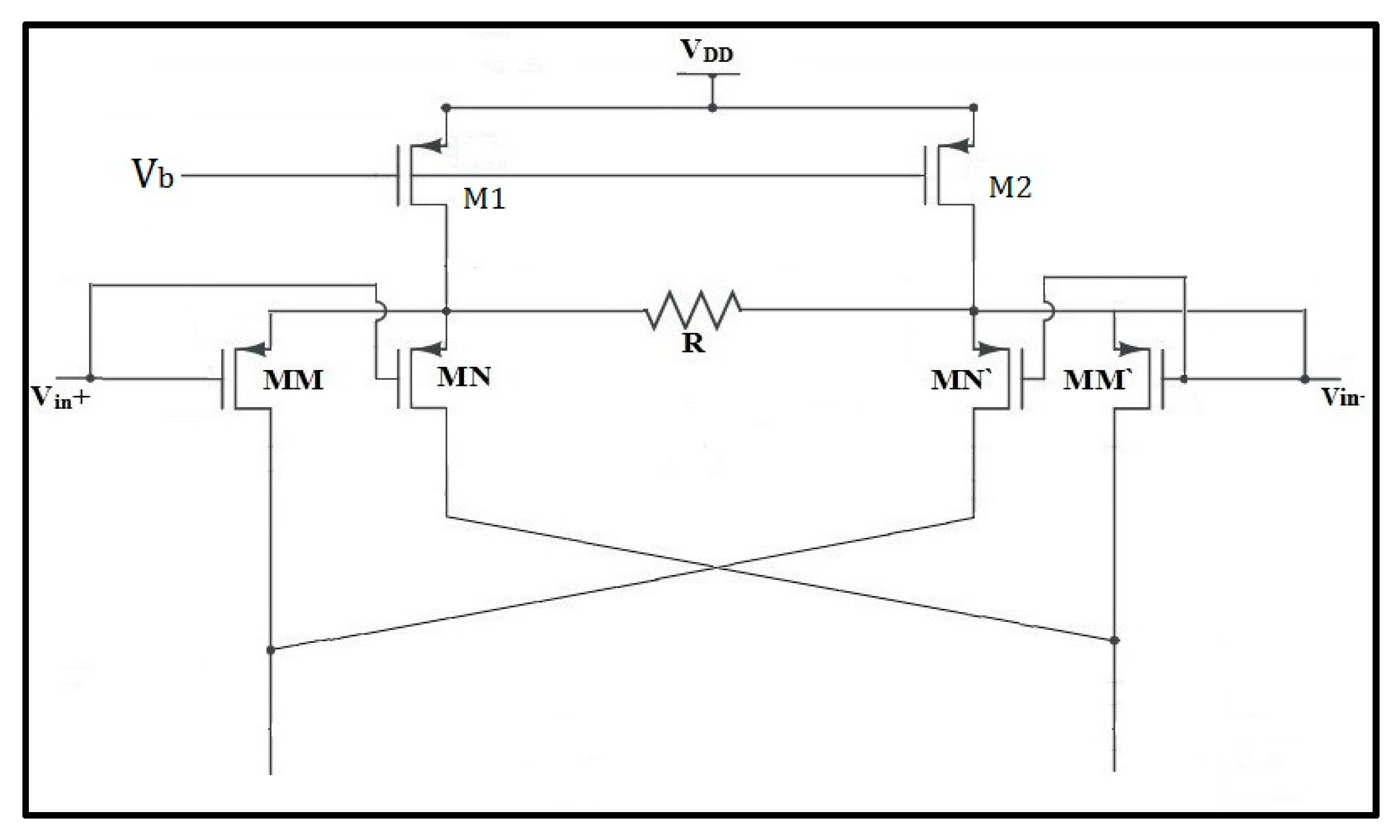
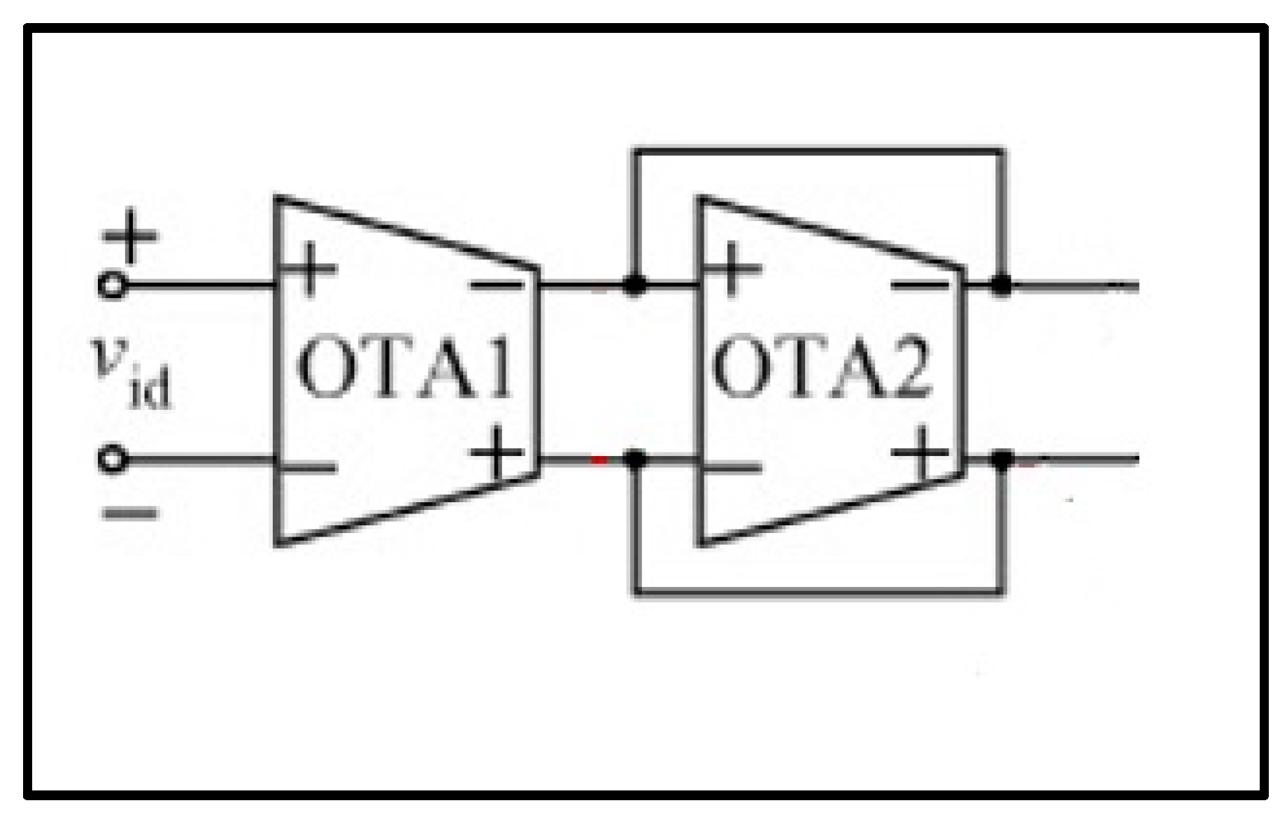
Figure 3 shows the block diagram of a fully differential OTA. The bulk driven input pairs are used with two cross coupled differential pairs to cancel out the non-linear component. A source degeneration resistor is used to increase the linearity. The small signal currents, ia and ib, flow through the transistors, M1 and M2, which are cross coupled, and the final currents, i1 and i2, are generated, which are copied by CM4, CM6 and CM1 to the output which provides a current (i2–i1) and CM3, CM5 and CM2 which produces the current (i1–i2) at the other output end. Figure 4 shows the detailed schematic of the bulk driven, fully differential, self-cascode OTA.
The input part of the OTA comprises two bulk driven differential pairs, cross coupled with the opposite pair to cancel the non-linear term. The source is degenerated with the help of a resistor to improve the linearity, which is the simplest, best option for the circuit. Bulk driven MOS are selected to reduce the supply voltage, as the threshold voltage does not appear in the signal path. Two different currents, ia and ib, flow, depending upon the sizes through the two differential pairs, which then get added at the cross coupled node and form currents i1 and i2, at nodes Vda and Vdb, respectively. The currents from the cross coupled differential pair, i1, are then copied by the diode connected self-cascode load, M7, M8, to the current mirrors, M17, M18 and M11, M12, through current mirrors, M15, M16 and M13, M14. Similarly, current i2, from the loads M5 and M6, is mirrored to M9, M10 and M19, M20 through current mirrors, M23, M24 and M21, M22. The output node, i+, provides a current, i1–i2 and the opposite output end, i-, provides the current, i2–i1. The current gains of all the current mirrors are set to 1. The OTA circuit input comprises a total of eight branches, out of which two branches are from the input pairs, two branches are from the two current mirrors and the remaining two are from the output branch. The input part should be properly optimized so that an optimized gain, phase and GBW with a low total harmonic distortion (THD) should be achieved. The output part consists of common source drivers, M5, M6 and M7, M8, with their self-cascode loads, M21, M22 and M13, M14. The designed OTA utilizes a self-cascode structure instead of a normal cascode because self-cascode structures provide high output impedances and save a Vth drop, compared to conventional cascodes [30]. All the transistors are operated in the subthreshold region to ensure a power efficient circuit suitable for low voltage, low frequency, portable biomedical applications.
Fully differential structures always require a common mode feedback circuit (CMFB) to stabilize the common mode output voltage, but this proposed OTA is based on current mirrors which have an inherent common mode feedback. In general, the single ended output OTA and op-amp structures are the common mode signal, generated at the diode connected low-impedance nodes of the current mirroring MOS transistor; these are copied to the final output node in the first stage and the output common mode signal becomes well defined and it does not need the CMFB network (N/W). However, in a fully differential structure, the common gates of the output section, n-MOS or p-MOS, are biased by a constant DC voltage (V bias-n or V bias-p, respectively). The output nodes’ voltage (DC value) is not defined in this case, and it needs to be stabilized through a negative feedback-based CMFG N/W. However, in the case of the proposed OTA circuit, there exists two-subsections in the first stage. This is called a balanced OTA structure, in which both internal nodes are symmetrical low-impedance nodes, unlike the conventional single ended, output based nodes of the current mirror asymmetric OTA, where one node is of a high impedance and the other node is a low-impedance node. In the balanced, bulk driven, cross coupled-based, V/I converter (used in this design), both of the internal outputs’ (intermediate) nodes are low-impedance mode nodes, where there exists one p-MOS in a diode connected configuration, and the DC voltage generated there well defines both of the final differential output nodes’ (conveyed to output nodes for well-matched input section CMOS transistors) DC bias voltages correspondingly. So, a CMFB circuit is not mandatory for the balance or symmetrical structure of this circuit.
The dimensions of the transistor are listed in Table 1.
3. Performance Equation
This section is sub-divided into two sections: The first section shows the details of self-cascode composite transistors in the subthreshold region. The second section shows the derivation of the transconductance of the proposed OTA circuit.
3.1. Subthreshold Equation
The weak inversion current is an exponential function of the input voltage. The drain to source the current IDS of a transistor in the subthreshold region is given by
where,
The complete equation is
where represents the characteristic current and np is the slope factor in the weak inversion. VGS, VBS and VDS are the gate, bulk and the drain voltages, respectively. is the threshold voltage at VBS = 0 and is the thermal voltage in which K is the Boltzmann’s constant and q is the electric charge. is the characteristic current given by The transistor will be saturated in this region when . The gate transconductance in the subthreshold region is given by
This is a function of and whereas the bulk transconductance is a function of body effect coefficient, , and the Fermi potential, , which is given by
The bulk transconductance, , is 2–3 times less than the gate transconductance, , and it does not depend on the aspect ratios of MOSFETs, as it does in strong inversion.
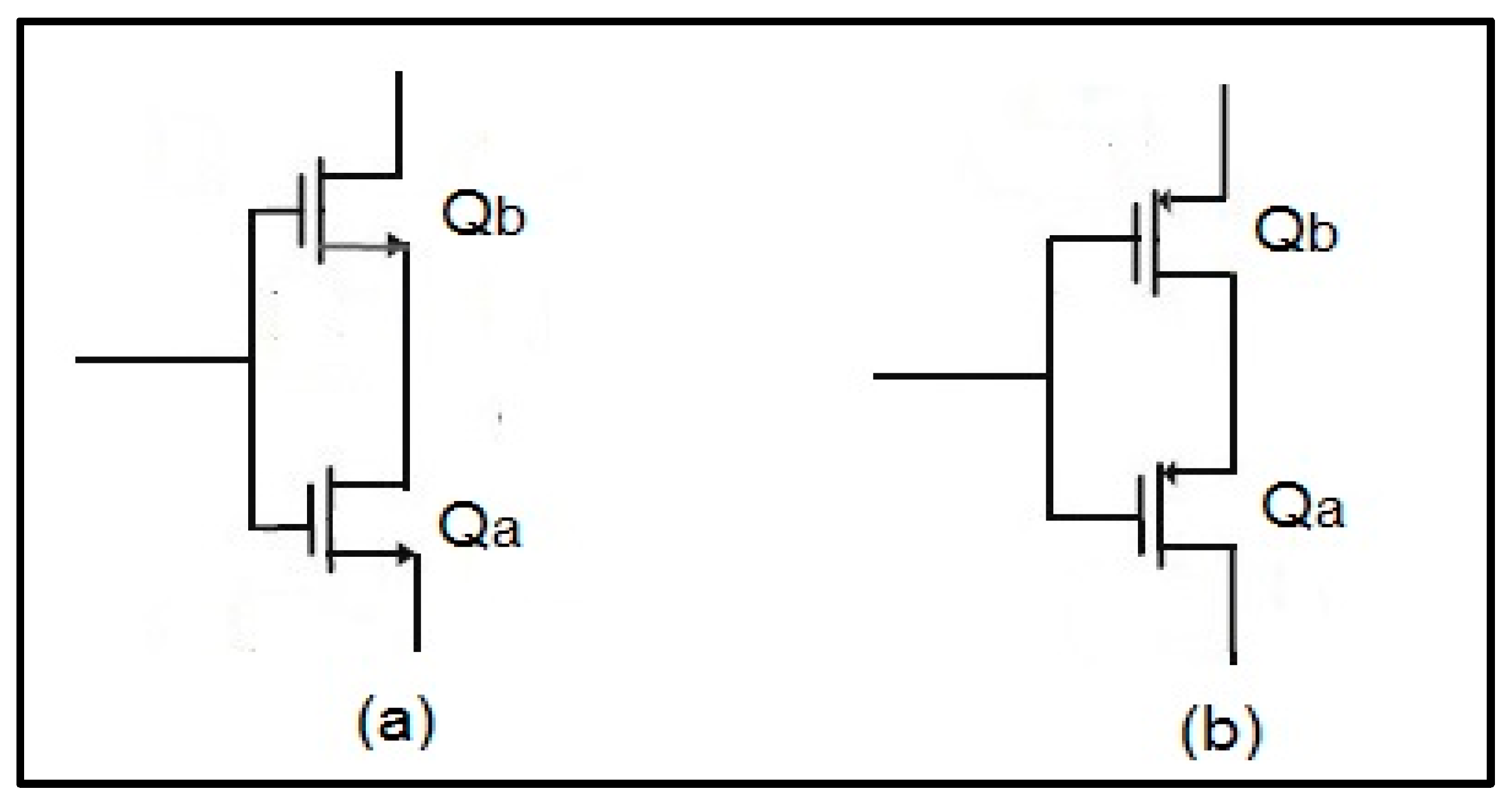
3.2. Composite MOS
The composite transistors, NMOS and PMOS, are shown in Figure 5 these are important configurations in weak inversion [13]. These self-cascode composite transistors are able to provide high output impedance and a lower Vth drop than a normal cascode; therefore, they is preferred for low voltage applications.
3.2.1. Sizing of Composite Transistors
Considering Figure 5a, the currents and voltages of the composite transistor can be derived and written as
where, and are the drains to source the current flowing through transistors Qa and Qb, is the drain to source the voltage of transistor Qa, and and are the gates to source voltages of transistors Qa and Qb, respectively. The transistor on the rail side is called the rail device and the transistor on the other side is called the cascode device [7]. Considering that both of the transistors are in the saturation region of weak inversion and are implemented in the same well, thereby causing a body effect, by solving Equations (2) and (9), the expression of can be written as [17,30]
The drain source voltage of transistor Qa is a logarithmic function of the transistor sizes, rather than the gate to source voltage, as in a conventional transistor. For both the transistors to be in the saturation region of weak inversion, . To maintain this condition, the sizes of the transistor should be set according to Equation (13).
The above condition shows that the size of transistor Qb should be at least greater than 19 times the size of transistor Qa. Therefore a large area is required to maintain the transistors in saturation [30]. The same condition applies to the PMOS composite transistor as well.
3.2.2. Small Signal Model of Composite Transistors
Figure 6 shows the small signal model of the composite transistor from Figure 3a when both transistors are saturated. The output resistance is multiplied by the gain of the common gate amplifier; thus, it becomes larger for same value of VGS. The currents and voltages of the composite transistors are same as for a single transistor, and a small value of VDS is enough to saturate both the transistors, as long as the transistor ratios satisfy Equation (13). The composite transistor has biasing similar to a single MOS; therefore, it does not increase the power of the circuit and the purpose of the composite transistor is to increase the output impedance and thus the gain. The small signal equivalent equation is given by [15,30]:
And
3.2.3. Noise of Composite MOS
The noise of a composite MOS comprises of flicker noise and thermal noise, which can be given by the following expression [11]:
Total noise can be calculated as a single MOS transistor.
3.3. Transconductance of OTA
In regard to the simplified block diagram of the OTA shown in Figure 7, the input transistor pair gate is grounded, and the input signal is applied to the bulks. The grounded gates provide an inversion layer, and a current (Ib) flows through the input pairs, even if no input signal is applied and no current flows through the degeneration resistor. If a small signal differential voltage is applied at the bulk of the differential pairs and V1 is greater than V2, then a current (iR) will flow through the source degeneration resistor (Rs). This current can be expressed as
Considering the simplified half circuit and its small signal model of Figure 8, N represents the transconductance ratio between M2 and M4. The transconductance of the OTA is given by [31,32]:
where, ( = ) = is the effective bulk transconductance of the differential pairs, is the conductance of the source degeneration resistance. N shows that the size of the transistor M2 is N times M4. The transconductance of the differential pair is decreased by a factor of (1 + N) and depends on Rs.
Further simplifying Equation (22),
Equations (23) and (24) show that is linear to the conductance, . Thus, by increasing Rs, linearity is increased at the cost of decreased transconductance.
4. Simulation Results
The proposed OTA was simulated in CADENCE virtuoso environment using LFoundry 150 nm CMOS process parameters. Different simulation graphs were extracted from CADENCE and plotted on MATLAB software using CSV files. The objectives of the different simulations were to obtain various performances of the OTA with respect to ac response, transient response, corner simulation and the DC sweep.
4.1. AC Response
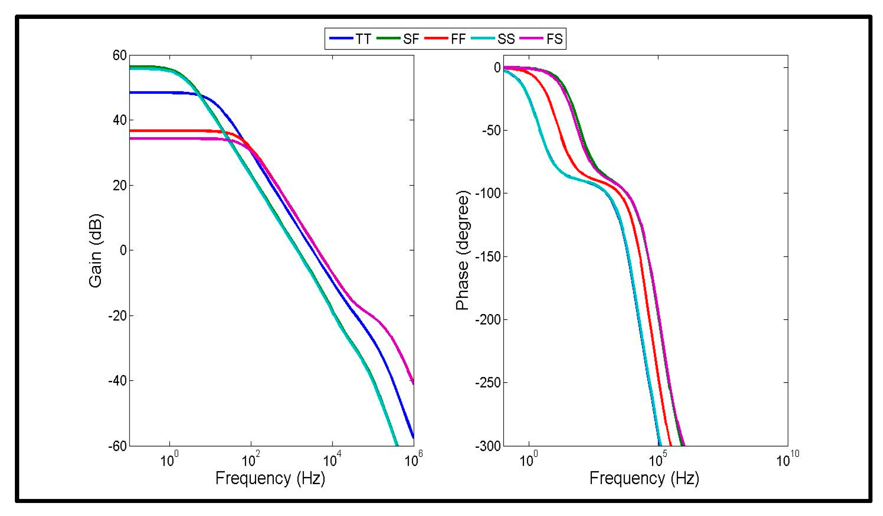
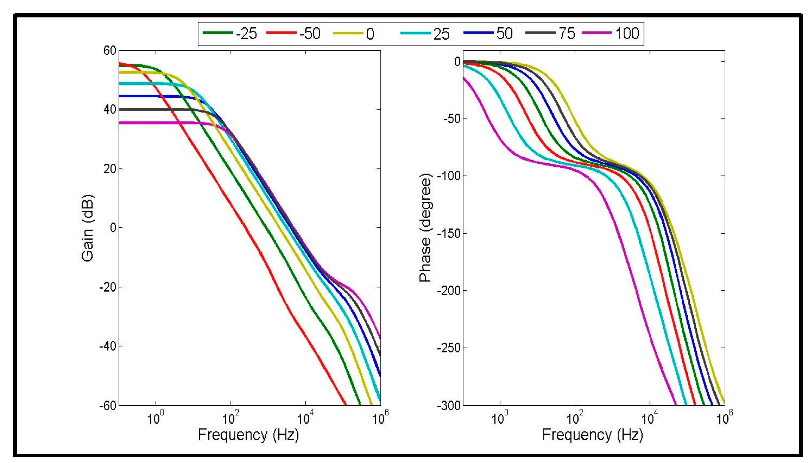
The AC analysis of the proposed OTA was done with a capacitive load of 1 pF and the DC gain obtained was 48.4 dB with a unity gain bandwidth (GBW) of 3.1 KHz; the phase margin (PM) and gain margin (GM) were found to be 80° and 19.01 dB, respectively. The gain was improved from 32 dB to 48 dB by using the composite MOS. The GBW can be improved further by keeping the current mirrors (CM) ratio high, but here in the proposed OTA, the CM ratio was kept at 1:1, as for low frequency circuits, the GBW is usually low. The gain and phase responses of the proposed OTA are shown in Figure 9 along with various corner simulations at the four corners (i.e., slow NMOS, slow PMOS (SS); slow NMOS, fast PMOS (SF); fast NMOS and slow PMOS (FS); and lastly fast NMOS and fast PMOS (FF)). Figure 10 shows the effect of temperature variation on the ac gain and phase response. The designed circuit must be capable of working under device tolerance, temperature and process variations, and device mismatch effects. The process corners were simulated to check the robustness of the circuit.
Table 2 shows the simulation results of the ac analysis under process corners. The performance deviations at the four corners regarding the gain, GBW, PM and GM lie in the range of 34–56 dB, 1.3 K–4.3 K, 76.5°–83.5° and 19–20.5 dB, respectively, whereas the gain, GBW, PM and GM for a TT (typical typical) case are 48.4 db, 3.1 KHz, 80° and 19.01 dB, respectively.
To verify that the designed circuit works properly in different environmental conditions, the effect of temperature variations, from −50° to 100 °C, on the above-mentioned parameters of the ac response, are shown in Table 3.
4.2. Common Mode Rejection Ratio (CMRR)
The common mode rejection ratio (CMRR) is the ability of a differential amplifier to reject the common mode signal (i.e., signals common to both inputs). CMRR can be calculated as
where, is the differential gain and is the input common mode gain.
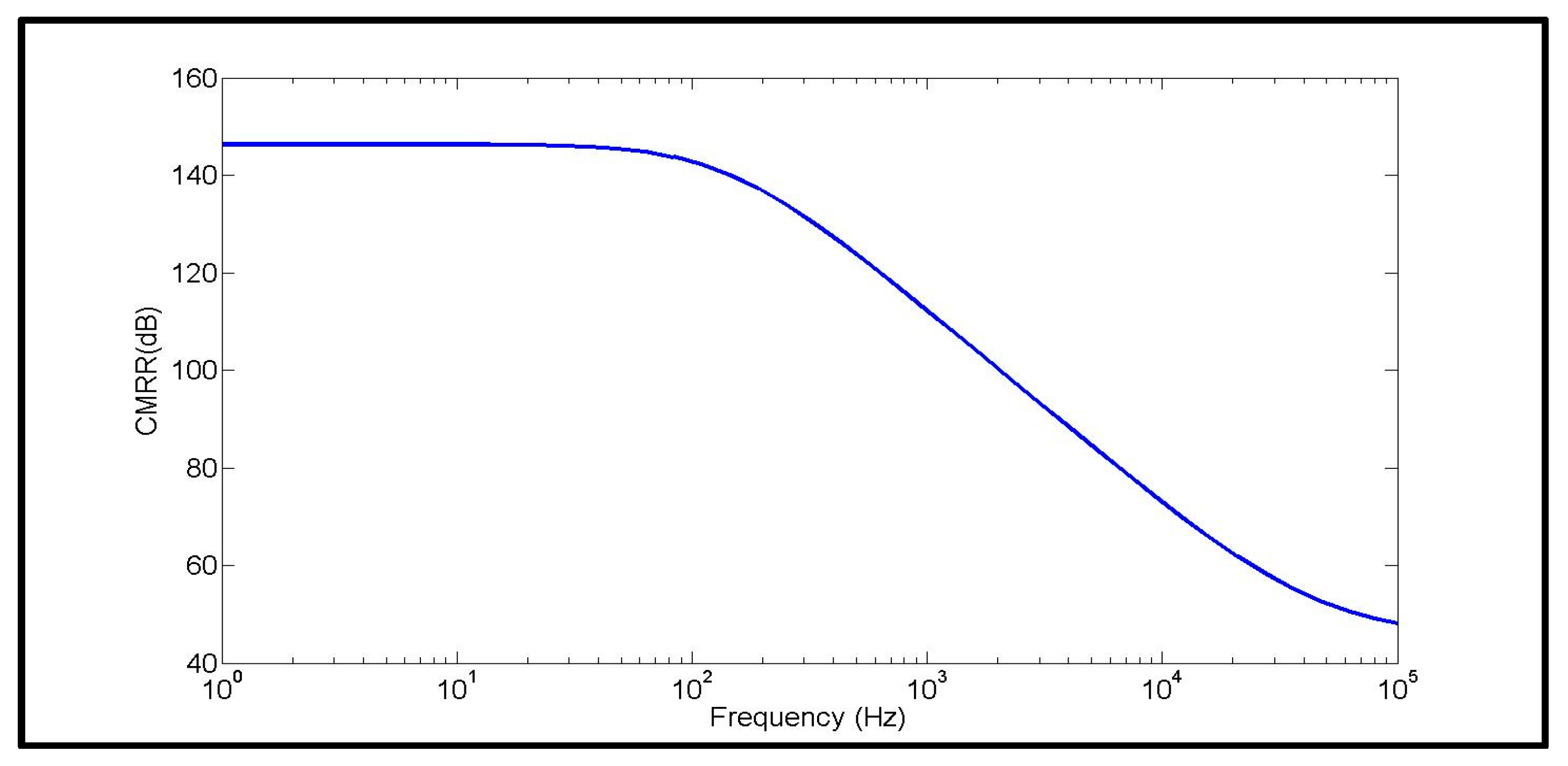
Figure 11 shows that the CMRR is 146.3 dB, which is high at low frequencies and starts to decrease as differential gain decreases and common mode gain increases. Various common mode noises can be rejected by having good noise immunity, and this can be achieved by having a higher CMRR: the higher the CMRR, the lower the effect of the common mode signal.
4.3. Power Supply Rejection Ratio (PSRR)
The power supply rejection ratio (PSRR) is the ability of a device to maintain its output voltage as the DC power supply voltage (VDC) varies. It can be expressed as
where, is the differential mode gain and A+ is the ratio of differential voltage to the change in power supply. A+ can be expressed as
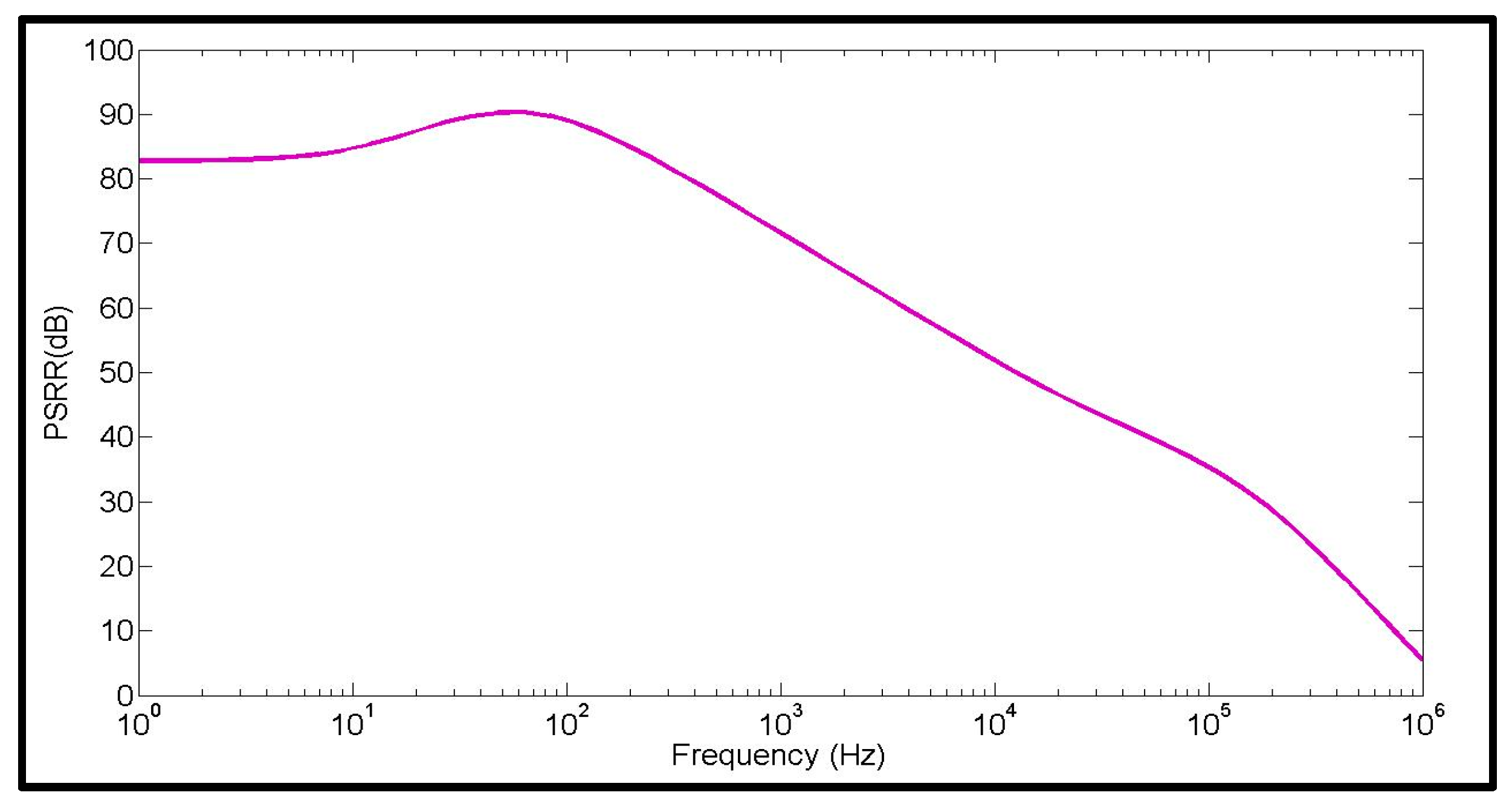
Figure 12 shows that a PSRR of 83 dB is obtained at low frequencies. Higher PSRR values are required to reduce the effect of ripples generated due to the variation in power supply.
4.4. Slew Rate (SR)
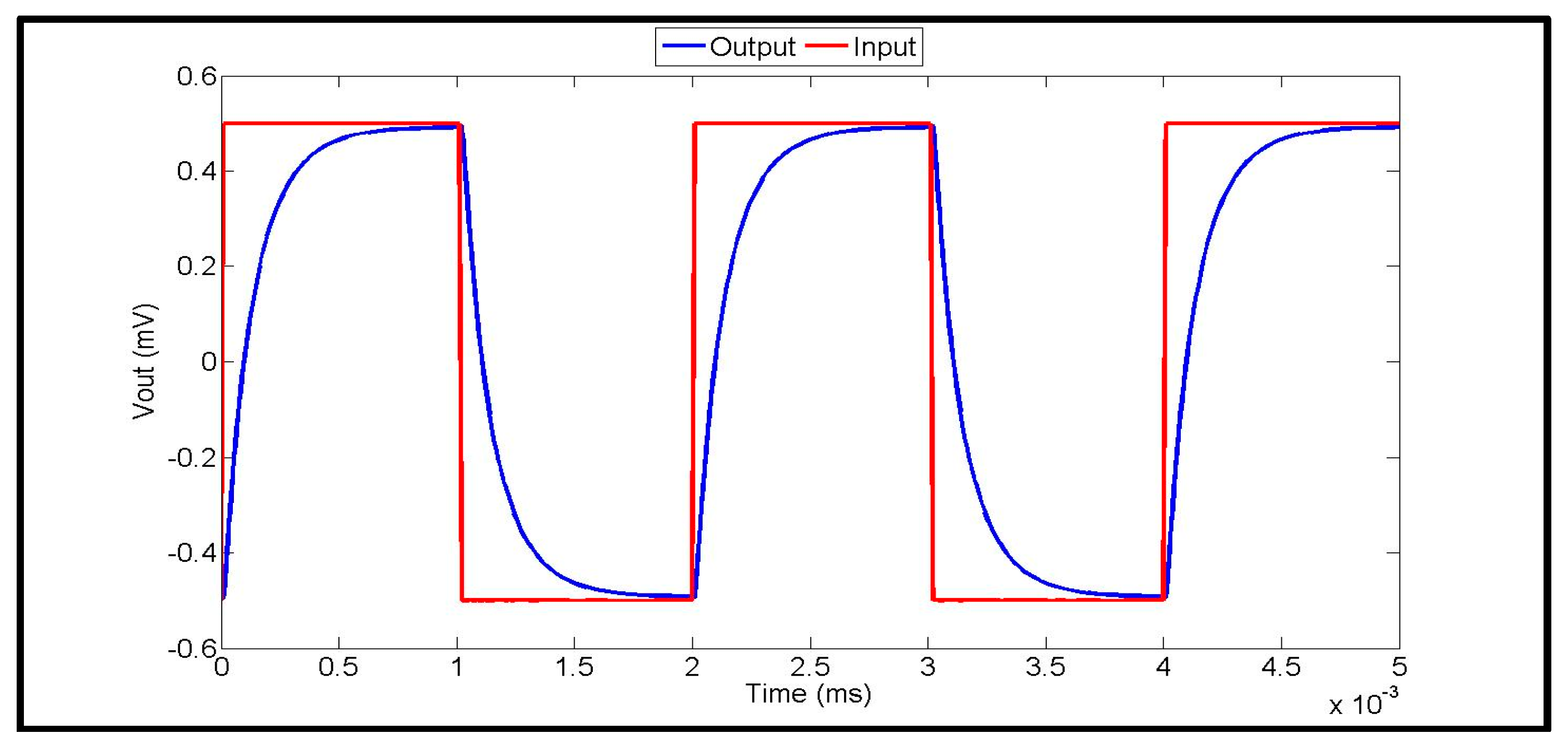
The slew rate is the rate of change of output voltage with respect to the input voltage. The proposed circuit is operated in thte subthreshold region which requires a very low current, which decreases the slew rate and slows down the speed of OTA. However, the capacitor value is kept smaller than 1 pF which maintains the slew rate at a desirable value. Figure 13 shows the response of the OTA when an input is applied with a 1 Vpp square wave. The positive SR (SR+) is 99.56 V/ms and the negative SR (SR−) is 100 V/ms.
4.5. Transient Response
The transient response of the OTA with the differential input signal and the differential output signal is shown in Figure 14. The transient response of the OTA was simulated in a unity gain configuration using the setup shown in Figure 15. The transient response was performed with an input signal of 200 mVpp at a frequency of 100 Hz.
4.6. Transconductance
The transconductance of the OTA for low frequency applications should be very low—usually in the order of few nA/V—to obtain the low cut-off frequency which is required in biomedical devices. A trade off exists for lower values of Gm; there is increased input referred noise levels which can be minimized by properly sizing the input differential pairs. The sizes of the input transistors are kept larger because larger sizes, particularly in terms of length, reduce the flicker noise, which, in turn, reduces the input referred noise [27,33]. The transconductance obtained is 23 nA/V with a linear range of +/− 100 mV, which is shown in Figure 16.
4.7. Total Harmonic Distortion (THD)
The total harmonic distortion (THD) is a measurement of the harmonic distortion present in a signal and is defined as the ratio of the sum of the powers of all harmonic components to the power of the fundamental frequency. The total harmonic distortion (THD) is obtained by applying a sinusoidal input of 200 mVpp at a frequency of 100 Hz. The achieved THD is −58.56 dB, which is shown in Figure 17. Second harmonics are suppressed due to the differential nature of the circuit.
Figure 18 shows the differential output current versus frequency plot, showing the linear range of the OTA with respect to the output current.
4.8. Power Consumption
The DC analysis of OTA was carried out in an open loop configuration to check the condition involving saturation in the weak inversion region . The currents in each branch are 11 nA and the total current consumed by the overall circuit is 74 nW with a supply voltage of 0.8 V. Therefore, the overall power consumption of the OTA is 59.04 nW.
5. Discussion
Different simulation results were shown in the above section to prove that a considerable linearity can be achieved by using the source degeneration technique, bulk driven and cross coupled differential pairs to improve the THD. Bulk driven transconductance is lower than that of the gate driven technique, but this low transconductance is favorable for our circuit, because this circuit focuses on low frequency biomedical applications. The transconductance obtained was 23 nA/V. The currents in each branch were 11 nA and the total current consumed by the overall circuit was 74 nW. A low power of up to 59.04 nW can be obtained for portable devices, and this power can be further reduced if the supply voltage is reduced to 0.6 V (circuit works well), but the dynamic range can also be reduced, which can reduce the signal to noise ratio (SNR) of the circuit, so the supply voltage was kept at 0.8 V. The highest CMRR was achieved which shows that the input common mode signal has a low effect, and it proves that the proposed OTA has good noise immunity and is able to reject various common mode noises. PSRR was also obtained to find the effect of ripples generated due to variation in power supply. The slew rate obtained was 99.56/100 V/ms, which is comparatively low because the circuit operated in the subthreshold region and in this region, currents are very low, which limits the speed of OTA. Different corner simulations have been executed to check the effect of variations on gain, GBW, GM, PM; not only this, but temperature variations were also observed. The PM remained stable around 80° which shows that the circuit is quite stable, even at different corners. The performance deviation at the four corners with respect to gain, GBW, PM and GM values lay in the ranges of 34.24–56.32 dB, 1.3–4.3 K, 76.5–83.5° and 19.01–20.5 dB, respectively, whereas the gain, GBW, PM and GM values for a TT (typical typical) case are 48.4 db, 3.1 KHz, 80° and 19.01 dB, respectively. A comparison of these results with the results available in the literature is shown Table 4.
From Table 4, it can be seen that a high CMRR, low power, greater PM and low THD were achieved and were found to be favorable, compared to the results available in the literature. Due to the differential nature of the structure, even harmonics were suppressed and the odd harmonics were reduced by using cross coupled differential pairs, which helps in achieving a low THD below 55 dB. The technology used was 150 nm which is a reduced size compared to others in the literature. The circuit works well up to a supply voltage of 0.6 V, which can further reduce the power up to 44.2 nW, but the output swing will be reduced for such low voltages; therefore, the supply voltage was kept at 0.8 V. To compare the proposed work with state of the art technologies, a figure of merit (FOM) was adopted, which can be calculated by
The designed OTA circuit can be used in different applications, such as amplifiers, filters, oscillators, data converters, etc. In terms of portable biomedical applications, it can be used in ECGs, EEGs, EMGs, neural recording networks, etc., as its power consumption is low which makes it suitable for portable devices.
6. Conclusions
This paper presented the design of a fully differential, bulk driven OTA. The OTA comprised a source degeneration MOS with a cross coupled differential pair to improve linearity. The bulk driven technique was used to improve linearity and to reduce the supply voltage which removes the threshold voltage from the signal path. Source degeneration and cross coupled techniques reduced the transconductance which is favorable for our circuit because low transconductance is required for low frequency applications. The transconductance obtained was 23 nA/V. A low voltage and low power were obtained by operating the transistors in the subthreshold region, which is one of the best options to make the circuit power efficient. The gain, GBW, PM and GM values obtained were 48.4 dB, 3.1 KHz, 80° and 19.01 dB, respectively. Different corner simulations were performed to check the robustness of the circuit. Temperature effects were also observed on the ac response. The CMRR, PSRR and slew rate+/− values were 146.3 dB, 83 dB and 99.56/100 V/ms, respectively. The circuit utilizes self-cascode composite transistors to enhance the output resistance and thus the gain, from 32 dB to 48 dB; the self cascode MOS does not require any biasing circuitry and provides a Vth drop that is less than that of a conventional MOS. The power of the circuit was also reduced by up to 59.04 nW with a supply voltage of 0.8 V. The THD obtained was −58.56 dB for an input signal of 200 mVpp at a frequency of 100 Hz. FOM was also calculated to compare the proposed work with state of the art technology, and FOM was calculated as 254.13. The circuit was simulated in CADENCE virtuoso environment using 150 nm LFoundry CMOS process. The obtained results prove that the circuit is suitable for low voltage, low power and low frequency applications.
Author Contributions
Saleha Bano contributed to the idea, design and implementation of the simulation steps. Ghous Bakhsh Narejo and Syed Muhammad Usman Ali Shah contributed in drafting and reviewing the final form.
Conflicts of Interest
The authors declare no conflict of interest.
Appendix A
To clearly understand the terms used in this paper a tabulated form of acronyms are included which is shown in Table A1.

Table A1.
Acronyms.
| Acronyms | Definition |
|---|---|
| OTA | Operational transconductance amplifier |
| THD | Total harmonic distortion |
| FOM | Figure of merit |
| BD | Bulk driven |
| GD | Gate driven |
| GBW | Gain bandwidth |
| GM | Gain margin |
| PM | Phase margin |
| SR | Slew rate |
| CMRR | Common mode rejection ratio |
| PSRR | Power supply rejection ratio |
| SNR | Signal to noise ratio |
| LV | Low voltage |
| LP | Low power |
References
- Rakus, M.; Stopjakova, V.; Arbet, D. Design techniques for low voltage analog integrated circuits. J. Electr. Eng. 2017, 68, 245–255. [Google Scholar] [CrossRef]
- Raj, N.; Sharma, K.; Jasuja, A.; Gard, R. A low power OTA for biomedical applications. Cyber J. Multidiscip. J. Sci. Technol./J. Sel. Areas Bioeng. 2010, 1–5. [Google Scholar] [CrossRef]
- Wang, T.-Y.; Liu, L.-H.; Peng, S.Y. A power efficient highly linear reconfigurable bio-potential sensing amplifier using gate balanced Pseudo resistors. IEEE Trans. Circuits Syst. II Express Briefs 2015, 62, 199–203. [Google Scholar] [CrossRef]
- Chakraborty, A. Low power low voltage operation of operational amplifier. Int. J. Res. Eng. Technol. 2015, 4, 297–300. [Google Scholar]
- Yodtean, A.; Thanachayanont, A. Sub 1-V highly linear low power class AB bulk driven tunable CMOS transconductor. Analog Integr. Circuits Signal Process. 2013, 73, 383–397. [Google Scholar] [CrossRef]
- Hogervorst, R.; Huijsing, J. Design of Low-Voltage, Low-Power Operational Amplifier Cells, 3rd ed.; Springer: Dordrecht, The Netherland, 2000; pp. 1–206. ISBN 978-1-4757-2489-9. [Google Scholar]
- Sharan, T.; Bhadauria, V. Fully differential, bulk driven, class AB, sub-threshold OTA with enhanced slew rates and gain. J. Circuits Syst. Comput. 2017, 26, 1750001. [Google Scholar] [CrossRef]
- Sharan, T.; Chetri, P.; Bhadauria, V. Ultra-low-power bulk-driven fully differential subthreshold OTAs with partial positive feedback for Gm-C filters. Analog Integr. Circuits Syst. 2018, 94, 427–447. [Google Scholar] [CrossRef]
- Carrillo, J.M.; Torelli, G.; P-Aloe, R.; Valverde, J.M.; D-Carrillo, J.F. Single-pair bulk driven CMOS input stage: A compact low-voltage analog cell for scaled technologies. Integr. VLSI J. 2010, 43, 251–257. [Google Scholar] [CrossRef]
- Raikos, G.; Vlassis, S. 0.8V bulk driven operational amplifier. Analog Integr. Circuit Signal Process. 2010, 63, 425–432. [Google Scholar] [CrossRef]
- Carvajal, R.G.; R-Angulo, J.; L-Martin, A.J.; Torralba, A.; Galan, J.A.G.; Carlosena, A.; Chavero, F.M. The flipped voltage follower: A useful cell for low voltage low power circuit design. IEEE Trans. Circuits Syst. I 2005, 52, 1276–1291. [Google Scholar] [CrossRef]
- Rodriguez-Villegas, E.; Yufera, Y.; Reuda, A. A 1.25V micropower Gm-C filter based on FGMOS transistor operating in weak inversion. IEEE J. Solid State Circuits 2004, 39, 100–111. [Google Scholar] [CrossRef]
- Lo, T.-Y.; Hung, C.C. A 1-V 50 MHz pseudo differential OTA with compensation of mobility reduction. IEEE Trans. Circuits Syst. II 2007, 54, 1047–1051. [Google Scholar] [CrossRef]
- Szczepanski, S.; Pankiewicz, B.; Koziel, S.; Wojcikowski, M. Multiple output differential OTA with linearized bulk driven active-error feedback loop for continuous time filter applications. Int. J. Circuit Theory Appl. 2015, 43, 1671–1686. [Google Scholar] [CrossRef]
- Cotrim, E.D.C.; Ferreira, L.H.C. An ultra-low-power CMOS symmetrical OTA for low-frequency Gm-C applications. Analog Integr. Circuits Signal Process. 2012, 71, 275–282. [Google Scholar] [CrossRef]
- Khateb, F.; Biolek, D.; Khatib, N.; Vávra, J. Utilizing the Bulk-driven technique in analog circuit design. In Proceedings of the IEEE 13th International Symposium on Design and Diagnostics of Electronic Circuits and Systems (DDECS), Vienna, Austria, 14–16 April 2010. [Google Scholar]
- Ferreira, L.H.C.; Pimenta, T.C.; Moreno, R.L. An ultra–low-voltage ultra-low power MOS miller OTA with rail-to-rail input/output swing. IEEE Trans. Circuits Syst.-II Express Briefs 2007, 54, 843–847. [Google Scholar] [CrossRef]
- Sharan, T.; Bhadauria, V. Sub-threshold, cascode compensated, bulk driven OTAs with enhanced gain and phase margin. Microelectron. J. 2016, 54, 150–165. [Google Scholar] [CrossRef]
- Azhari, S.J.; Rezaei, F. High linear, high CMRR, low power OTA with class AB output stage. Int. J. Comput. Theory Eng. 2010, 2, 473–477. [Google Scholar] [CrossRef]
- Mincey, J.S.; Briseno-Vidrios, C.; Martinez, J.S.; Rodenbeck, C.T. Low-power Gm-C filter employing current re-use differential difference amplifiers. IEEE Trans. Circuits Syst. II Express Briefs 2017, 64, 635–639. [Google Scholar] [CrossRef]
- El Mourabit, A.; Lu, G.; Pittet, P. Wide linear range sub-threshold OTA for low power, low voltage and low frequency applications. IEEE Trans. Circuits Syst. I 2005, 52, 1481–1488. [Google Scholar] [CrossRef]
- Worapishet, A.; Naphaphan, C. Current feedback source degenerated CMOS transconductor with very high linearity. Electron. Lett. 2003, 39, 17–18. [Google Scholar] [CrossRef]
- Kwon, K.; Kim, H.T.; Lee, K. A 50–300 MHz highly linear and low noise CMOS Gm-C filter adopting multiple gated transistors for digital TV tuner ICs. IEEE Trans. Microw. Theory Tech. 2009, 57, 306–313. [Google Scholar] [CrossRef]
- Razaei, F.; Azhari, S.J. Transconductor linearization based on adaptive biasing of source degenerative MOS transistors. Circuits Syst. Signal Process. 2015, 34, 1149–1165. [Google Scholar] [CrossRef]
- Moreno, R.F.L.; Baruqui, F.A.P.; Petraglia, A. Bulk-tuned Gm-C filter using current cancellation. Microelectronics 2015, 46, 777–782. [Google Scholar] [CrossRef]
- Kim, D.; Kim, B.; Nam, S. A transconductor and tunable Gm-C high-pass filter linearization technique using feed forward Gm cancellation. IEEE Trans. Circuits Syst. II Express Brief 2015, 62, 1058–1062. [Google Scholar] [CrossRef]
- Lee, S.-Y.; Cheng, C.-J. Systematic design and modeling of OTA-C filter for portable ECG detection. IEEE Trans. Biomed. Circuits Syst. I 2009, 3, 53–64. [Google Scholar] [CrossRef] [PubMed]
- Abbasalizadeh, S.; Sheikhaei, S.; Forouzandeh, B. A 0.9 V supply OTA in 0.18 um CMOS technology and its application in realizing a tunable low-pass Gm-C filter for wireless sensor networks. Circuits Syst. 2013, 4, 34–43. [Google Scholar] [CrossRef]
- Sarrafinazhad, A.; Kara, I.; Baskaya, F. Design of a digitally tunable 5th order Gm-C filter using linearized OTA in 90 nm CMOS Technology. In Proceedings of the International Symposium on Signals, Circuits and Systems (ISSCS), Iasi, Romania, 9–10 July 2015. [Google Scholar]
- Ferreira, L.H.; Pimento, T.C.; Moreno, R.L. An ultra-low-voltage ultra-power weak inversion composite MOS transistor: Concept and applications. IEICE Trans. Fundamental Commun./Electron. Inf. Syst. 2002, E-85/A/B/C/D, 1–6. [Google Scholar] [CrossRef]
- Jihai, D.; Chuang, L.; Weilin, X.; Baolin, W. OTA-C filter for ECG acquisition systems with highly linear range and less pass band attenuation. J. Semicond. 2015, 36. [Google Scholar] [CrossRef]
- Soares, C.F.T.; de Maoraes, G.S.; Pertaglia, A. Low transconductance OTA with improved linearity suitable for low frequency Gm-C filters. Microelectronics 2014, 45, 1499–1507. [Google Scholar] [CrossRef]
- Sun, C.-Y.; Lee, S.-Y. A fifth order Butterworth OTA-C LPF with multiple output differential input OTA-C filter for ECG applications. IEEE Trans. Circuits Syst. II Express Brief 2017. [Google Scholar] [CrossRef]
- Akbari, M.; Nazari, M.; Sharifi, L.; Hashemipour, O. Improving power efficiency of a two stage operational amplifier for biomedical applications. Analog Integr. Circuits Signal Process. 2015, 84, 173–183. [Google Scholar] [CrossRef]
- Grasso, A.D.; Marano, D.; Palumbo, G.; Pennisi, S. Design methodology of subthreshold three-stage CMOS OTS suitable for ultra-low power low area and high driving capability. IEEE Trans. Circuit Syst. I 2015, 62, 1453–1462. [Google Scholar] [CrossRef]
- Akbari, M.; Hashemipour, O. A 0.6 V, 0.4uW bulk driven operational amplifier with rail to rail input/output swing. Analog Integr. Circuits Signal Process. 2016, 86, 341–351. [Google Scholar] [CrossRef]
Figure 1.
Cross coupled differential pair with source degeneration.

Figure 2.
Bulk driven differential pair.
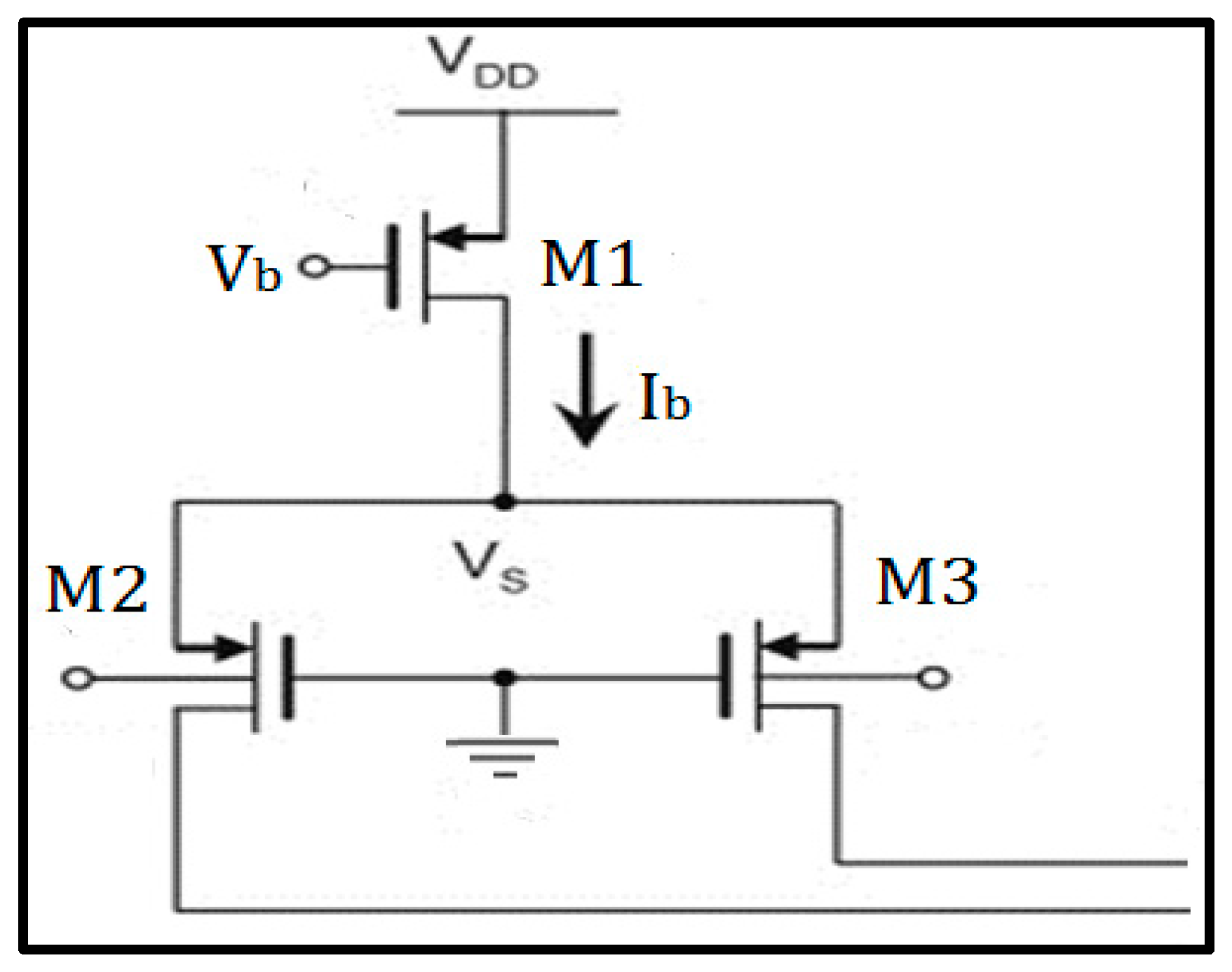
Figure 3.
Block diagram of the fully differential operational transconductance amplifier (OTA).
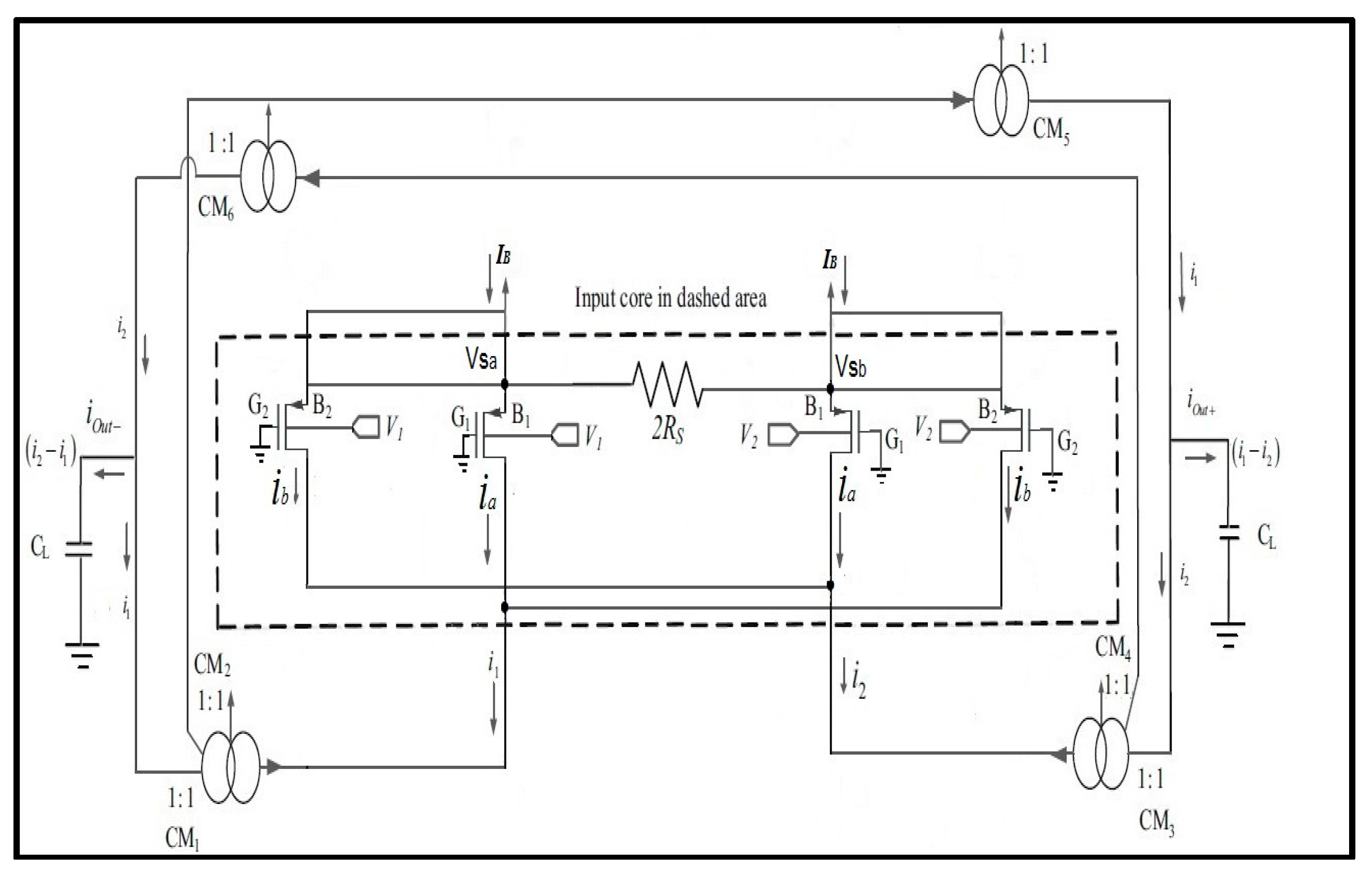
Figure 4.
Schematic of the bulk driven fully differential self-cascode OTA.
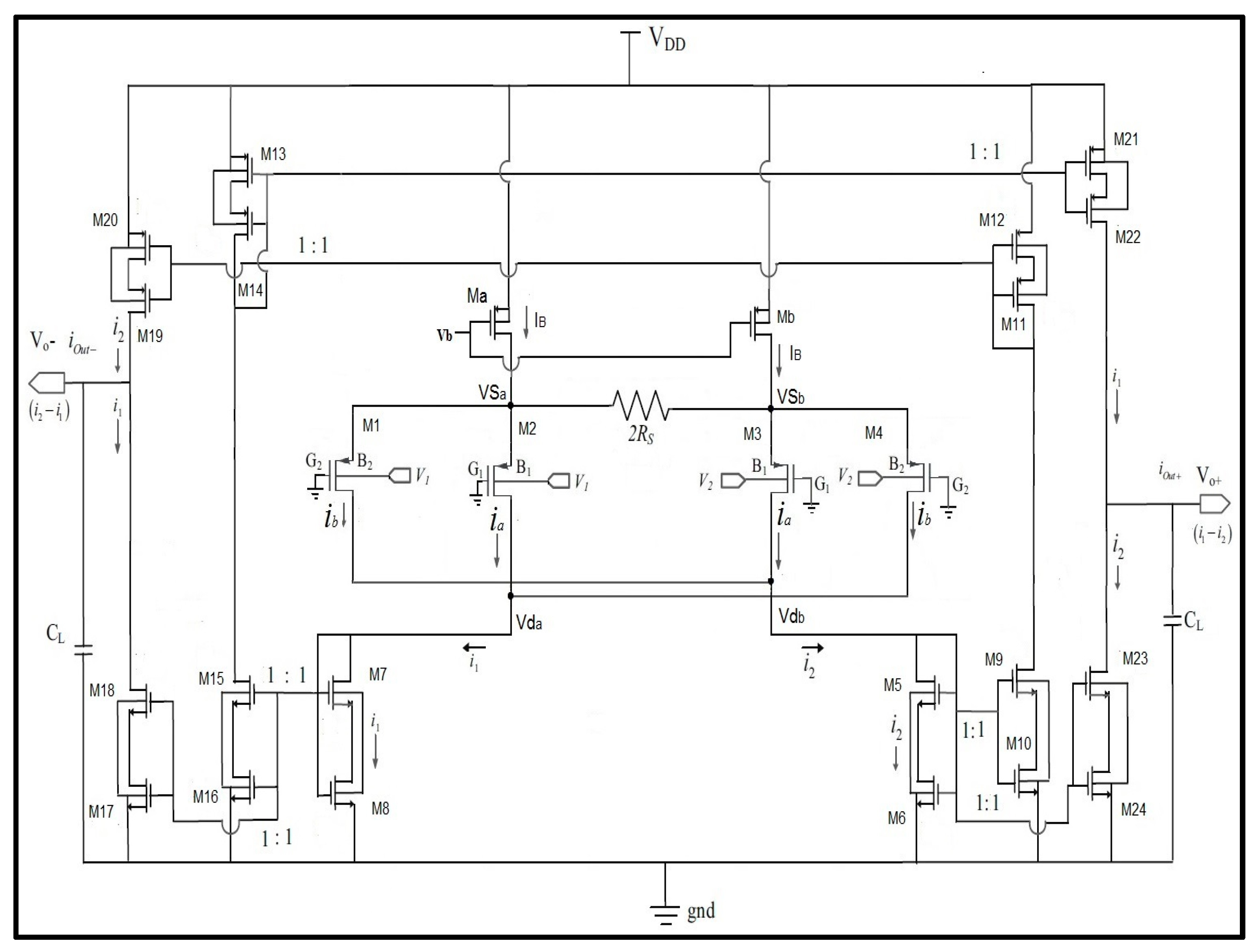
Figure 5.
(a) NMOS composite transistor (b) PMOS composite transistor.

Figure 6.
Small signal model of the composite transistor.
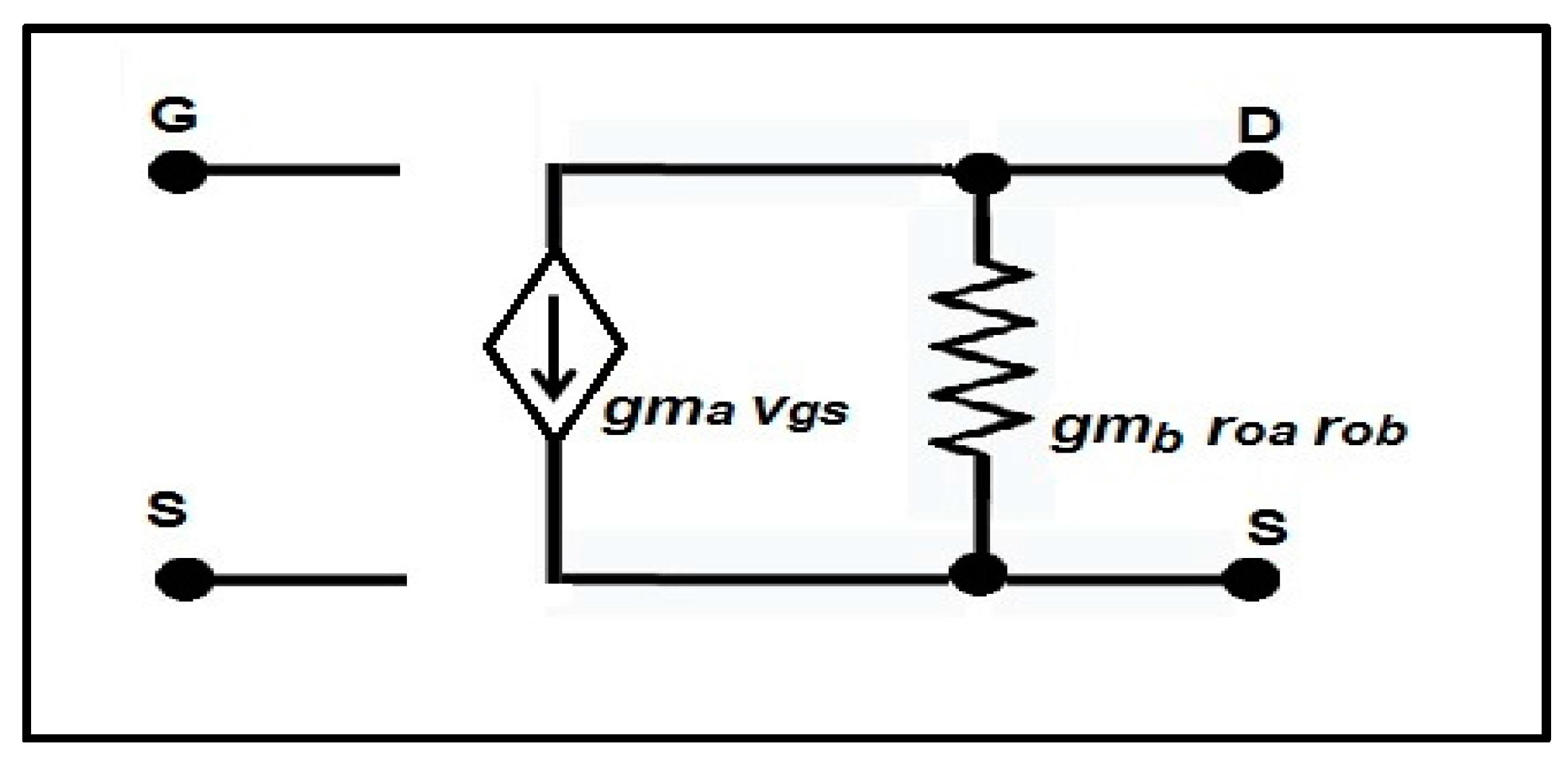
Figure 7.
Half circuit of the proposed OTA.
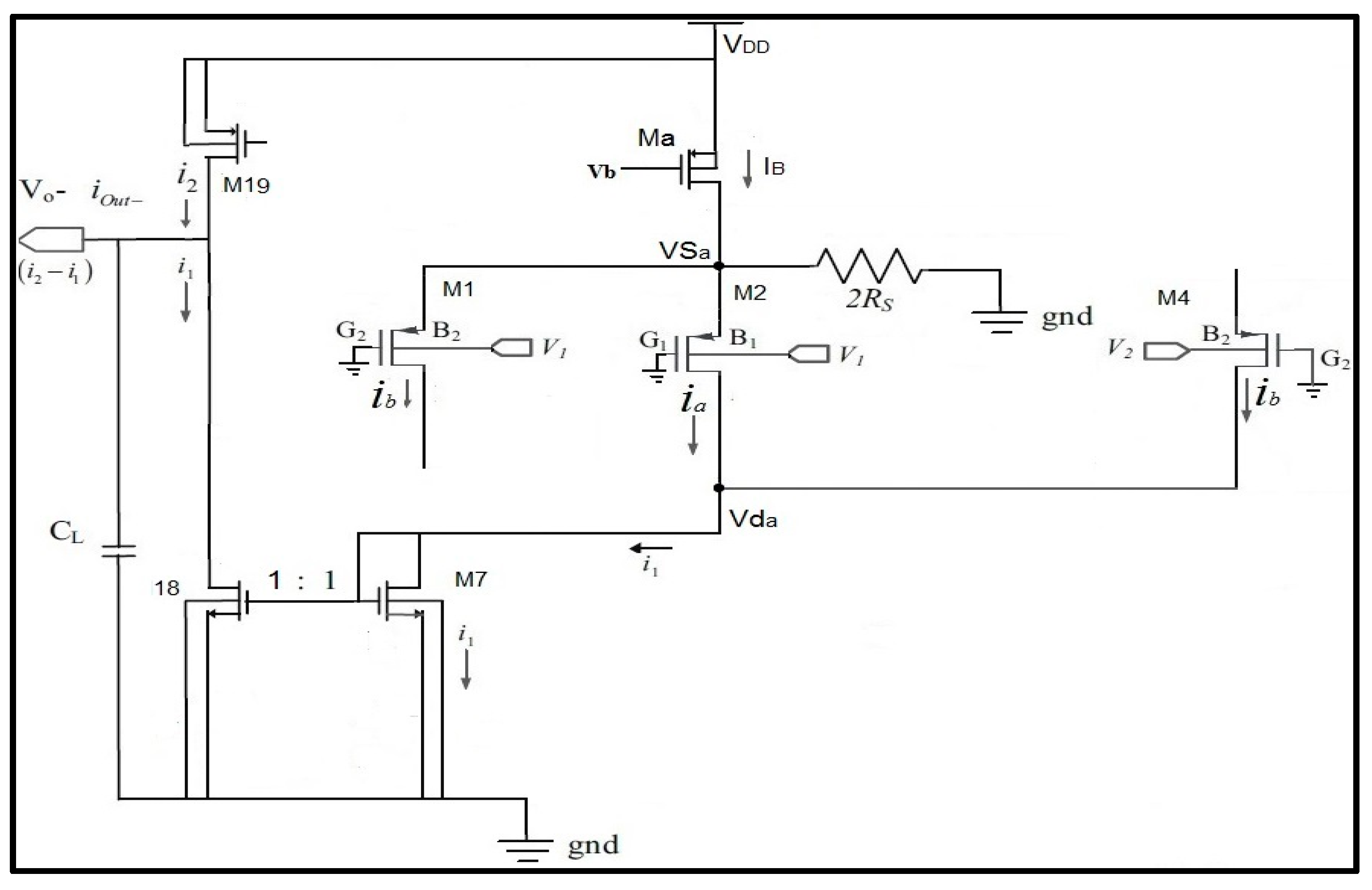
Figure 8.
Small signal model of the half circuit.
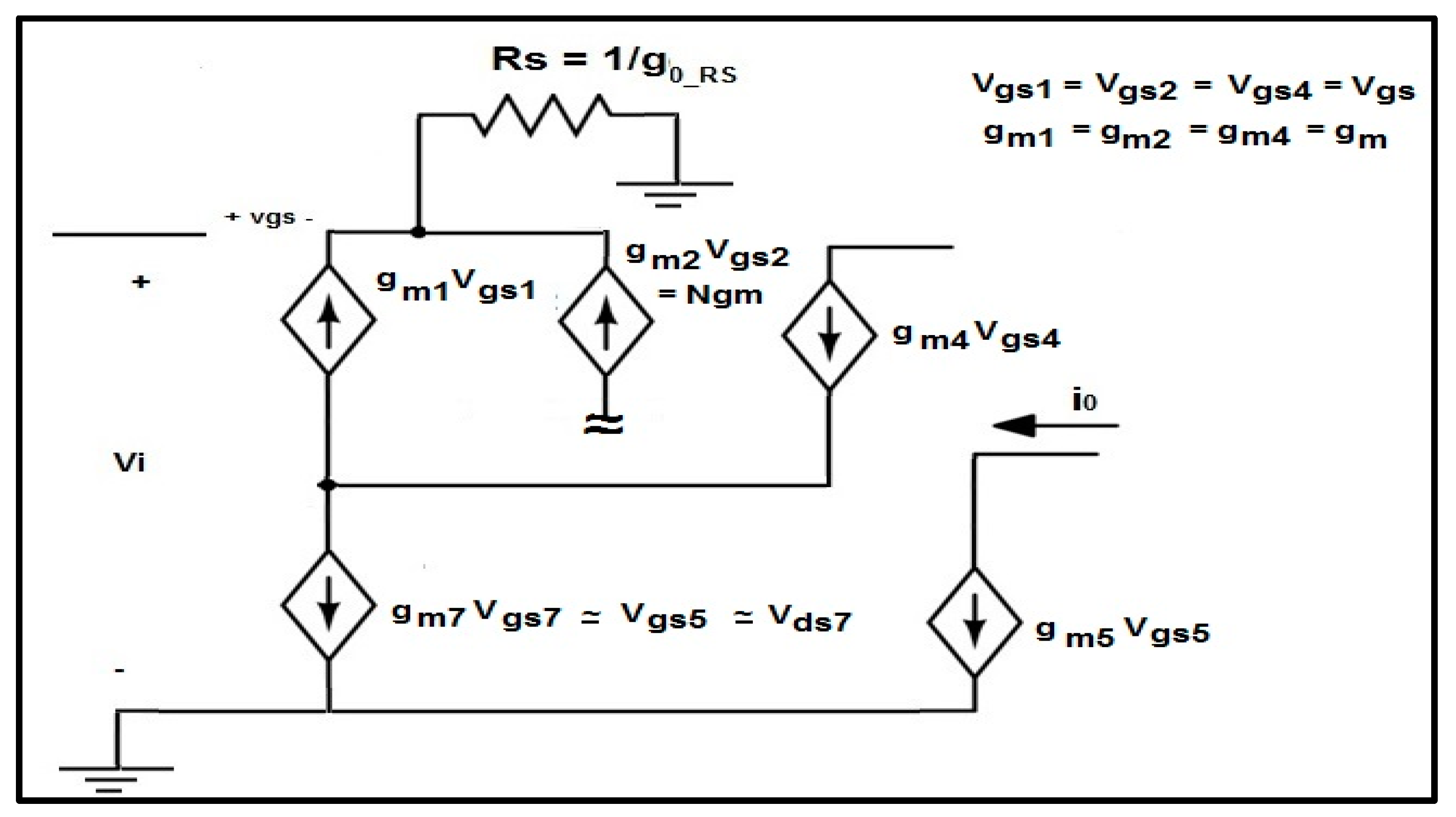
Figure 9.
Process corner effects on the ac gain and phase response.

Figure 10.
Temperature variation effects on the ac gain and phase response.

Figure 11.
The common mode rejection ratio (CMRR).

Figure 12.
The power supply rejection ratio (PSRR).

Figure 13.
Slew Rate.

Figure 14.
Transient response of the differential input and output.

Figure 15.
Setup for the fully differential to unity gain conversion.

Figure 16.
Transconductance plot of OTA.
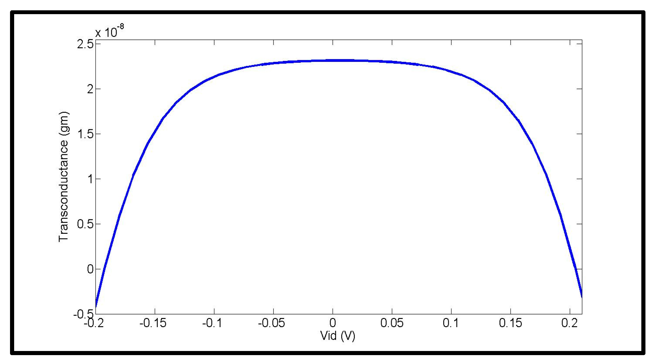
Figure 17.
Total harmonic distortion (THD) plot, applying a sinusoidal input of 200 mVpp at a frequency of 100 Hz.
Figure 17.
Total harmonic distortion (THD) plot, applying a sinusoidal input of 200 mVpp at a frequency of 100 Hz.
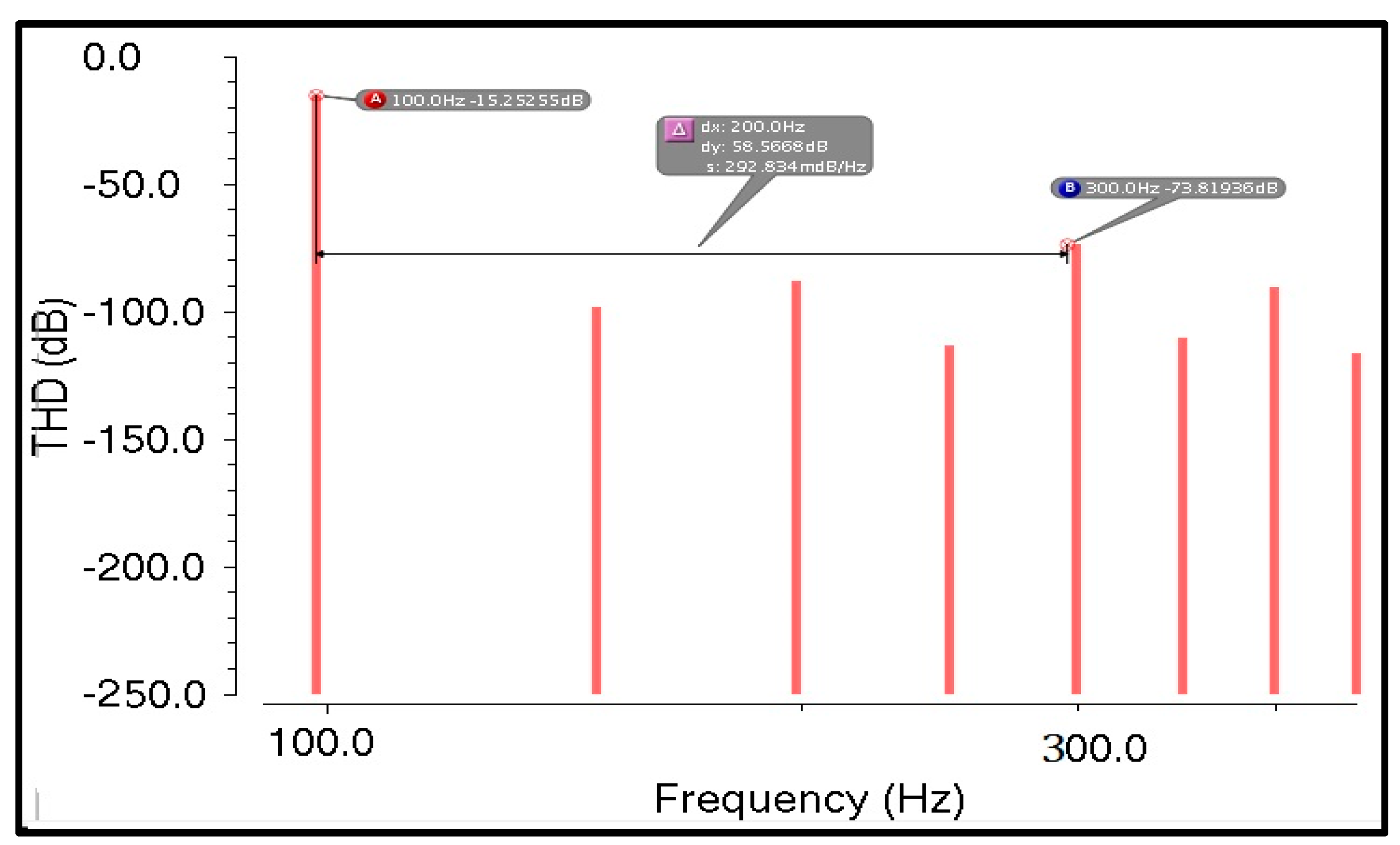
Figure 18.
Differential output current of OTA.
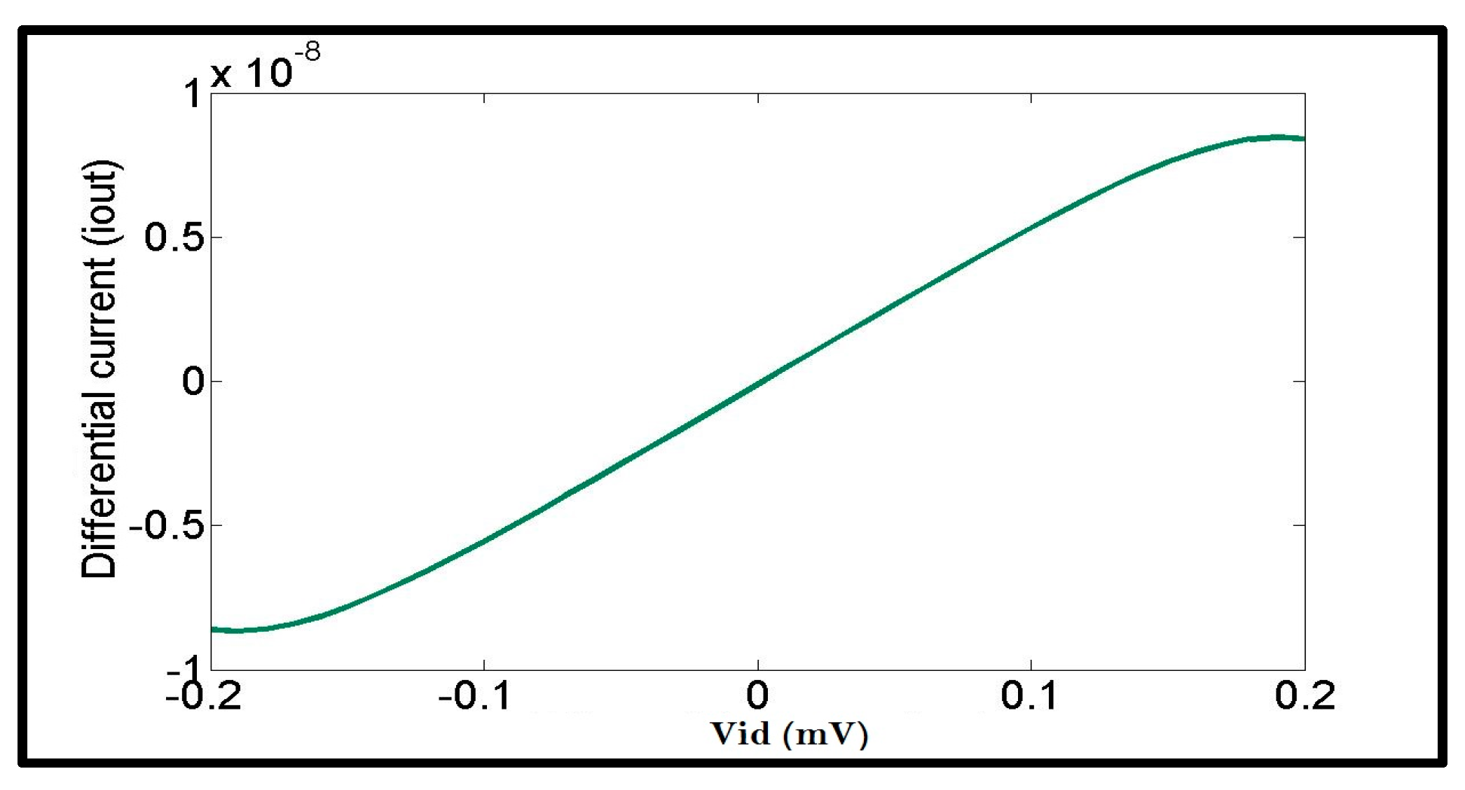
Table 1.
Transistor Dimensions.
| Transistors | W/L (um) |
|---|---|
| Ma, Mb | 1/0.5 |
| M1, M4 | 10/10 |
| M2, M3 | 30/10 |
| M5, M7, M9, M15, M18, M23 | 30/1 |
| M6, M8, M10, M16, M17, M24 | 1.5/1 |
| M12, M13, M20, M21 | 8/1 |
| MM11, M14, M19, M22 | 160/1 |
Table 2.
Effect of corners on ac response.
| Corner Name | Corner | Gain (dB) | GBW (Hz) | PM (degree) | GM (dB) |
|---|---|---|---|---|---|
| Nominal | TT | 48.40 | 3.1 K | 80° | 19.01 |
| C0 | SS | 55.78 | 1.3 K | 76.5° | 20.4 |
| C1 | SF | 56.32 | 1.4 K | 78.6° | 20.5 |
| C2 | FS | 34.24 | 4.2 k | 83.5° | 19.2 |
| C3 | FF | 36.67 | 4.3 K | 83.3° | 19.3 |
Table 3.
Effect of temperature variation on the ac response.
| Temperature (°C) | Gain (dB) | GBW (Hz) | PM (degree) | GM (dB) |
|---|---|---|---|---|
| −50 | 55.4 | 234.7 | 78.5° | 25.2 |
| −25 | 54.84 | 866.5 | 77.8° | 22.1 |
| 0 | 52.48 | 1.9 K | 77.5° | 20.1 |
| 25 | 48.72 | 2.9 K | 79.9° | 18.9 |
| 50 | 44.38 | 3.8 K | 81.1° | 18.7 |
| 75 | 40 | 4.4 K | 82.1° | 18.9 |
| 100 | 35.4 | 4.7 K | 83.4° | 18.8 |
Table 4.
Comparison of the different parameters of the OTA in the current study with different OTAs available in the literature.
Table 4.
Comparison of the different parameters of the OTA in the current study with different OTAs available in the literature.
| Parameters | This Work [2018] | [2017] Ref [7] | [2015] Ref [34] | [2015] Ref [35] | [2015] Ref [36] |
|---|---|---|---|---|---|
| Technology (nm) | 150 nm | 180 nm | 180 nm | 350 nm | 180 nm |
| Topology | BD (D) | BD (D) | GD (D) | GD (S) | BD (S) |
| Stages | Single | Single | Two | Three | Two |
| VDD | 0.8 V | 0.5 V | 0.6 V | 1 V | 0.6 V |
| Gain (dB) | 48.4 dB | 70.4 dB | 90.1 dB | 120 dB | 82 dB |
| GBW (Hz) | 3.1 KHz | 9.24 KHz | 34.9 KHz | 20 KHz | 19.1 KHz |
| GM (dB) | 19.01 dB | 19.5 dB | 20 dB | - | - |
| PM (degree) | 80° | 54° | 62.2° | 54° | 60° |
| CMRR (dB) | 146.3 dB | 106 dB | 37 dB | 70 dB | 114.7 dB |
| PSRR (dB) | 83 dB | 70 dB | 30.7 dB | 184 dB | |
| SR+/− (V/ms) | 99.56/100 | 967 | 7.5 | 7.38/2.88 | 5.6 |
| Power (W) | 59.04 nW | 64 nW | 300 nW | 195 nW | 400 nW |
| THD (dB) | −58.56 dB | −52.4 dB | −40 dB | Less as SE | −55.9 dB |
| Cap. load (pF) | 1 pF | 2 × 15 pF | 2 × 7.5 pF | 200 pF | 15 pF |
| FOM | 254.13 | 9828.5 | 78.6 | 90.83 | 21.92 |
where BD and GD represent bulk driven and gate driven topologies, respectively. S and D represent the single ended and fully differential structures, FOM represents figure of merit and VDD represents the supply voltage.
© 2018 by the authors. Licensee MDPI, Basel, Switzerland. This article is an open access article distributed under the terms and conditions of the Creative Commons Attribution (CC BY) license (http://creativecommons.org/licenses/by/4.0/).
Share and Cite
MDPI and ACS Style
Bano, S.; Narejo, G.B.; Ali Shah, S.M.U. Power Efficient Fully Differential Bulk Driven OTA for Portable Biomedical Application. Electronics 2018, 7, 41. https://doi.org/10.3390/electronics7030041
AMA Style
Bano S, Narejo GB, Ali Shah SMU. Power Efficient Fully Differential Bulk Driven OTA for Portable Biomedical Application. Electronics. 2018; 7(3):41. https://doi.org/10.3390/electronics7030041
Chicago/Turabian StyleBano, Saleha, Ghous Bakhsh Narejo, and Syed Muhammad Usman Ali Shah. 2018. "Power Efficient Fully Differential Bulk Driven OTA for Portable Biomedical Application" Electronics 7, no. 3: 41. https://doi.org/10.3390/electronics7030041
Note that from the first issue of 2016, this journal uses article numbers instead of page numbers. See further details here.