1. Introduction
Biological solid-state devices have attracted more and more interest in recent years due to their promising advantages such as massive parallelism, power efficiency, adaptivity to complex non-linear computations, and high tolerance towards defects and variability [
1,
2]. For brain science, the synapse is the fundamental unit in neuromorphic systems, and therefore, to study the imitation of biological synapse is a critical first step toward neuromorphic computing. In previous research, conventional von Neumann digital computers software simulation and silicon complementary metal-oxide-semiconductor (CMOS) logic circuits were selected to implement artificial neural networks. However, these architectures lacked synapses’ intrinsic advantages in processing well-defined biological behavior, and instead were incomparable with biological systems in terms of space, speed and energy efficiency [
3,
4]. Large chip area and high power dissipation became blocks to the application of transistor-based neuromorphic system architectures, since ten transistors are required to mimic the function of each biological synapse at least. Additionally, data storage and computation are separated in von Neumann digital architecture and result in intrinsic delay during data transfer, which influence the computation speed. Therefore, it is more feasible to emulate the biological synapse in single solid-state devices with their inherent memory and computing abilities.
Recently, memristor has been widely investigated for next-generation nonvolatile memory (NVM) in embedded and stand-alone applications due to its advantages such as simple device structure, excellent scalability, fast program/erase speed and low power consumption. It is worth noting that the typical two-terminal metal-insulator-metal (MIM) structure of memristor is similar to synapses in a biological brain, and its high-density three-dimensional (3D) cross-point integrated architecture is compatible with neuromorphic systems in the biological brain. In addition, memristors with bipolar switching behaviors could analog memory characteristic by offering multi-level conductance states. These memristors have been proposed as attractive candidates to emulate synaptic functions in biologically inspired neuromorphic systems due to their multi-level conductance states [
5,
6,
7]. So far, a wide variety of materials including metal oxides, metal nitrides, metal-oxide nano-laminates and organics have shown synaptic behaviors [
8,
9,
10,
11,
12,
13]. Among these materials, few of them were compatible with CMOS process. A systematic study of the memristor operating as a biological synapse with CMOS compatible materials and fabrication processes are still lacking. HfO
2, as a high-k materials with resistive switching characteristics, has the potential to be used as the functional layer of synaptic devices [
14,
15,
16], and could well be compatible with the traditional CMOS process and play an important role in the process of device scaling.
In this paper, we develop comprehensive abilities of biological synapse in HfO2-based synaptic devices. Highly uniform HfO2 were fabricated by atomic layer deposition (ALD) method, which enable device sizes capable of scaling to nanoscale. Besides, HfO2 has superior electrical properties and excellent thermal and chemical stability, as well as being one of the preferred high-k gate dielectric materials in CMOS technology. High-density HfO2-based memristive devices can be successfully integrated with conventional CMOS technology. According to this work, synaptic devices with Ag active electrodes show comprehensive biological synapse abilities with lower power consumption. Short-term plasticity (STP), long-term potentiation/depression, spike-timing-dependent plasticity (STDP) and other properties of biological synapses were achieved with a series of electrical diagnosis scheme. These precisely electronic synapse behaviors are derived from the oxidation and reduction of metallic Ag between electrodes. This CMOS compatible HfO2-based synaptic devices show high potential to form an artificial neuromorphic computing system.
3. Result and Discussion
A synapse is the fundamental unit in the biological brain for connection between adjacent neurons.
Figure 1a illustrates a biological synapse connecting two neurons and the schematic structure of equivalent an HfO
2-based synaptic device. The action potentials (spikes) are generated by one neuron, propagate through the axon and are transmitted to the next neuron through the synapses. The typical two-terminal HfO
2-based metal-insulator-metal (MIM) structure is similar to synapse in a biological neuromorphic system, and top and bottom electrodes of a synaptic device can be regarded as pre-synaptic and post-synaptic neuron, respectively.
The devices with Ag top electrode and TaN top electrode were evaluated through direct-current voltage sweeping. The initial synaptic devices show high resistance state (HRS). After an electroforming process, repetitive I-V characteristics were measured under proper compliance current. As shown in
Figure 1b,c, both Ag and TaN top electrode exhibit superior bipolar switching characteristics. Stable cycling switching ability with an ON-OFF ratio and over 10-year data retention are obtained (
Figure S1). The set and reset operation voltage distribution and power consumption are presented as histograms and statistical charts in
Figure 1d,e, respectively. The Ag/HfO
2/Pt devices exhibit much lower SET/RESET operation voltage and power consumption. The SET and RESET voltage ranges of the Ag/HfO
2/Pt devices were from 0.21 to 0.37 V and from −0.1 to −0.15 V, while those of the TaN/HfO
2/Pt devices were from 1.3 to 1.8 V and from −1.3 to −1.5 V. The average power consumption was 0.1/0.02 mW in Ag/HfO
2/Pt devices, while it was 1.6/1.2 mW in TaN/HfO
2/Pt devices.
Moreover, a pulse-driven switching test was also implemented in TaN/HfO
2/Pt devices; these devices exhibit excellent pulse endurance properties at the nanosecond level (
Figure S2). As superior data storage reliability and ultra-fast programming speed, it is clear that HfO
2-based devices with TaN top electrode seems more suitable for NVM application, while Ag/HfO
2/Pt devices exhibit lower power consumption and multi-level resistance states (
Figure S3), which offer more advantages in neuromorphic computing application.
To further clarify the switching mechanism of the two types, HfO
2 based devices, the I-V curves were analyzed in
Figure 2a–d. The current transportation in both low resistance state (LRS) and high resistance state (HRS) exhibit ohmic current at positive and negative electrical field in Ag/HfO
2/Pt devices. For TaN/HfO
2/Pt devices, the LRS exhibits quasi-ohmic current (slope is approximately equal to 1) at positive electric field. However, the HRS exhibits ohmic, quasi-ohmic and space charge limited current along with an increasing electric field. Similar current transport mechanisms were observed with negative voltages. These results indicated that the stochastic and avalanching generation and recombination of oxygen ion and oxygen vacancy in the HfO
2 layer result in the forming and rupture of conducting filaments in TaN/HfO
2/Pt devices, which induce ultra-fast switching characteristics in TaN/HfO
2/Pt devices. In Ag/HfO
2/Pt devices, the forming and rupture of conducting filaments derive from the oxidation and reduction of metallic Ag, which can be driven by a much lower electric field.
Figure 3 shows the schematic illustration of the evolution of the metallic Ag filament formation and rupture in Ag/HfO
2/Pt synaptic devices. These Ag/HfO
2/Pt synaptic devices correspond to conventional electrochemical memory (ECM) cells [
17]. Under a positive bias, the active Ag is oxidized into Ag
+ ions at the Ag top electrode, and then, the migration and accumulation of those Ag
+ ions happened toward the Pt cathode. Finally, the Ag
+ ions are reduced to Ag conductive filaments across the HfO
2 dielectric layer. Therefore, these Ag/HfO
2/Pt synaptic devices exhibit an ohmic transport mechanism in the LRS state (set process). The diameter of Ag filament can be modulated by regulating the value of compliance current, thus multi-level resistance states can be realized in Ag/HfO
2/Pt synaptic devices (
Figure S3). When a negative bias is applied to the top Ag electrode, the oxidation of Ag filaments into Ag
+ ions and reduction at the Ag electrode occurred, which leading to the rupture of the filament conduction path and switching these devices to an OFF-state (reset process).
Synaptic plasticity is widely considered as the major cellular mechanism during learning and memorization in the biological brain. To mimic the abilities of synaptic plasticity comprehensively is the key feature of electron synaptic devices [
18,
19,
20,
21]. Synaptic plasticity illustrates the dynamic change of connection strength (synaptic weight) between biological neurons under electric spikes, and it can be classified into short-term and long-term plasticity (STP and LTP). STP means the duration of the potentiation of synaptic weight ranging from a few seconds to a few minutes. While for LTP, the potentiation of synaptic weight can last from hours to weeks or even years. However, STP can be converted to LTP through repeated rehearsals as well.
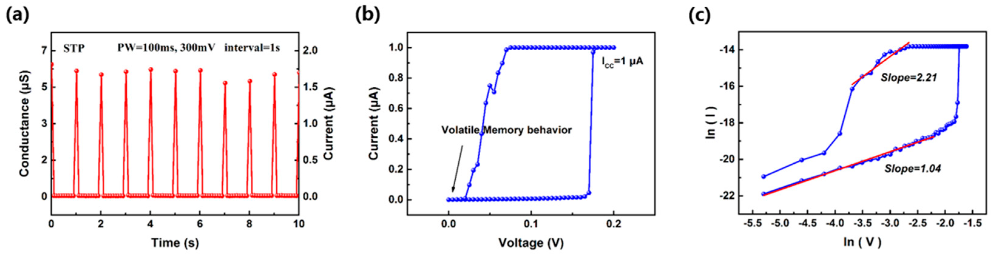
Figure 4a shows the STP properties of the Ag/HfO
2/Pt synaptic devices. To mimic the synaptic behaviors, 300 mV amplitude input pulse sequences with 100 ms pulse width and 1 s repetition interval were applied. An increase of conductance can be observed when a pulse arrived, and the conductance value reaches 5.7 μS (corresponding to a 1.7 μA output current). However, these devices cannot maintain its high conductance state and the conductance quickly decays to its initial conductance value during the relaxation duration of 1 s. This behavior corresponds to the STP behaviors in biological synapses. It is worth noting that the conductance value under the input pulse is lower than 77.5 μS, which is calculated approximately as the conductance value of one quantized channel. This phenomenon is attributed to the incomplete formation of Ag conductive filament. In order to further demonstrate this phenomenon, a DC I-V characteristic with a compliance current of 1 μA was measured. These devices show volatile memory behavior (shown in
Figure 4b).
Figure 4c shows the I-V characteristic in LRS and HRS. The current transportation in HRS exhibits an ohmic current, which is consists to the conclusion previous noted in this work. On the other hand, the current in LRS across the device is a space charge limited current. The threshold between different transport mechanisms in the LRS of the device is the conductance of one quantized channel. When the compliance current increase and the device conductance is over a constant value (77.5 μS), the devices exhibit an ohmic transport mechanism again in the LRS (shown in
Figure S3). Thus, STP behaviors converts to LTP ability in Ag/HfO
2/Pt synaptic devices.
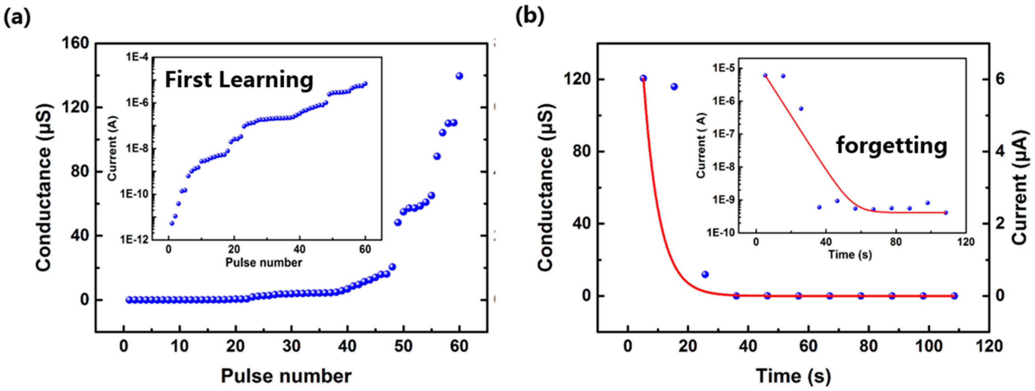
The “learning and forgetting” behaviors of a biological brain were also observed in Ag/HfO
2/Pt synaptic devices. As shown in
Figure 5a, input pulse sequences with a pulse number of 60, amplitude of 300 mV, 100 ms pulse width, and 100 ms intervals were applied to the fresh synaptic devices. The conductance gradually increases with the number of pulses, and saturates at 140 μS after the first “learning process”. When the applied pulse sequences are removed, a spontaneous decay of conductance occurs. The decay rate of conductance is fast at the initial state and then gradually slows down. Such a changing trend corresponds to the “human-memory forgetting curve” (
Figure 5b). Insets in
Figure 5a,b exhibit the “learning-experience” behavior on semi log coordinate. It is worth noting that the conductance of the synaptic devices does not relax to the initial state but rather stabilizes at an intermediate level. In the following “learning process”, less input pulse sequences are needed to produce the same amount of memory as the first “learning process”.
From a filamentary view, during the initial “learning process”, the conductance gradually increases due to the formation of a metallic Ag filament in the HfO2 layer. After learning, the Ag filament in Ag/HfO2/Pt synaptic devices is unstable, which is similar to the incomplete forming process during NVM application. After the “learning process”, the Ag filament is not dissolved completely. Thus, the conductance of Ag/HfO2/Pt synaptic devices remains in an intermediate level, and it can re-learn the forgotten information much easier through rehearsals.
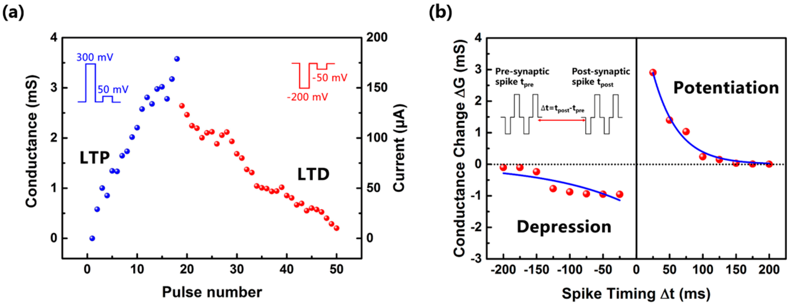
Figure 6a shows the measured long-term potentiation (LTP) and depression (LTD) curves using potentiating/depressing pulse sequences with an amplitude of 300 mV/−200 mV, a pulse width of 100 ms and a period of 250 ms. A read pulse with an amplitude of 50 mV/−50 mV, a pulse width of 100 ms was applied to measure the cell conductance followed every potentiating and depressing pulse, respectively. The conductance of Ag/HfO
2/Pt synaptic devices gradually increases with the stress of each potentiating pulse, and then gradually decreases with the following depressing pulses. The evolution of the conductance of Ag/HfO
2/Pt synaptic devices exhibits nonlinear behavior, and the change rate of conductance in the potentiating process is faster than in the depressing process. This could be due to the potentiating process being a positive feedback between the formation rate of metallic Ag filament, the temperature and local field strength [
22,
23], while the depressing process is a negative feedback and a slow decay of conductance can be observed.
Figure 6b shows the implementation of the STDP rule in Ag/HfO
2/Pt synaptic devices. The STDP rule is one of the important aspects in synaptic plasticity in a biological brain. The STDP rule can be understood as the change of synaptic weight dependence on the relative timing of pre-synaptic and post-synaptic spikes. If the pre-synaptic spike precedes a post-synaptic spike in arriving at the synapse (Δt > 0), the synaptic weight potentiation, corresponds to the increase of conductance. If the post-synaptic spike precedes pre-synaptic spike (Δt < 0), the synaptic weight depression, corresponds to the decrease of conductance. Furthermore, as the absolute value of Δt decreases, the amplitude of the change of synaptic weight increases. Both pre- synaptic and post-synaptic spikes contain a negative pulse with an amplitude of −200 mV in the beginning followed by a positive pulse with an amplitude of 300 mV. Each input pulse alone cannot modulate the conductance of Ag/HfO
2/Pt synaptic devices. When the pre-synaptic spike reaches the device earlier than the post-synaptic (Δt > 0), a conductance increase is observed. If Δt < 0, the conductance of Ag/HfO
2/Pt synaptic devices will decrease as well. The change of the conductance in the depression area is smaller than the potentiation one; it could be due to the inherent large resistive window in Ag/HfO
2/Pt devices which interfere with the visual presentation of the STDP rule on some level.


