TSV Technology and High-Energy Heavy Ions Radiation Impact Review

School of Electro-Mechanical Engineering, Xidian University, Xian 710071, China
*
Author to whom correspondence should be addressed.
Electronics 2018, 7(7), 112; https://doi.org/10.3390/electronics7070112
Submission received: 6 June 2018
/
Revised: 30 June 2018
/
Accepted: 4 July 2018
/
Published: 13 July 2018
Abstract
:Three-dimensional integrated circuits (3D IC) based on TSV (Through Silicon Via) technology is the latest packaging technology with the smallest size and quality. As a result, it can effectively reduce parasitic effects, improve work efficiency, reduce the power consumption of the chip, and so on. TSV-based silicon interposers have been applied in the ground environment. In order to meet the miniaturization, high performance and low-cost requirements of aerospace equipment, the adapter substrate is a better choice. However, the transfer substrate, as an important part of 3D integrated circuits, may accumulate charge due to heavy ion irradiation and further reduce the performance of the entire chip package in harsh space radiation environment or cause it to fail completely. Little research has been carried out until now. This article summarizes the research methods and conclusions of the research on silicon interposers and TSV technology in recent years, as well as the influence of high-energy heavy ions on semiconductor devices. Based on this, a series of research methods to study the effect of high-energy heavy ions on TSV and silicon adapter plates is proposed.
1. Introduction
Silicon interposers based on TSV (Through Silicon Via) technology are applied on the ground and in low-altitude environments to meet the needs of miniaturization, high performance and low cost of aerospace devices. However, in the high temperature difference, high impact and overload space environment, the silicon interposers being charged by high-energy heavy ions leads to damage of the insulating layer, the electromigration and heat transfer damage of RDL (redistribution layers), micro-bump and heterogeneous proton diffusion of the heterogeneous interface at the micro/nanosize. As a result, a series of problems like mechanical damage are caused.
2. Silicon Interposers and TSV Technology
With the development of the miniaturization, high performance and high reliability of electronic products, system integration is also increasing day by day. Under the circumstances, improving the performance by further reducing the feature size and interconnect line width of the integrated circuit is limited by the physical properties of the material and the process of the device. It becomes increasingly difficult for conventional 2-D SiP technology to keep up with Moore’s law due to the large parasitic resistance, inductance, and capacitance associated with long interconnects. A semiconductive wafer suitable for the fabrication of high frequency devices was invented by W. Shockley [1] in 1958 for the first time, which is considered as the first silicon interposer, includes closely spaced holes extending through it and was suitable for the fabrication of high frequency devices. A few years later, a thru-connection with an opening hole extending between opposite surfaces of a semiconductor wafer was invented by M.G Smith et al. [2], which opposite surfaces were connected ohmically to the degenerately doped portions to be electrically connected along the thru-connection. With further research and exploration, 2.5D/3D integration technology with TSV realized integrated circuits with advantages of high interconnection density, high performance, low power consumption, and low cost [3,4]. In addition, the core is widely considered to be the leading technology in the field of high density packaging in the future and is an effective way to break through Moore’s Law [5,6,7].
2.1. Silicon Interposer Production
People have made remarkable achievements in the production of silicon adapter plates today; however, the production process of interposers is becoming increasingly meticulous with the continuous improvement of integration and reduction of the package size. In recent years, scientists have conducted a series of research and optimization on the production process of silicon interposers.
Through-silicon via (TSV) is one of the most important parts for interposer system. In the traditional production process, TSV is first formed by Si etch and then filled by copper (Cu) plating. TSV is insulated by dielectrics to prevent short-circuit between metals and is covered by a thin barrier/seed layer for Cu plating [8,9,10,11]. Different processes have been used to deposit liner, such as thermal oxidation, plasma enhanced chemical vapor deposition (PECVD) and sub-atmospheric chemical vapor deposition (SACVD) [12,13]. Filling TSV is a very critical step for device reliability to ensure high breakdown voltage and low leakage current. There is some research devoted to relatively mature manufacturing processes and low cost to fully fill TSV. A high-cost and performance-effective passive silicon interposer was reported by Yao S. et al. [14]. A high-density and low-cost passive silicon interposer was proposed by Yook J.-M. et al. [15]. The mismatch in CTE (coefficient of thermal expansion) among TSV’s constituent materials will cause excess thermo-mechanical stress, which can eventually result in various reliability problems, such as open crack, interfacial delamination, and TSV protrusion [16,17]. Plenty of approaches have been proposed to minimize the stress. Annular TSV, with less stress and better reliability, shows great application potential for a simpler manufacturing process. In addition, research has been reported [18,19,20,21] predicting the cycle life and modelling the electrical and mechanical. A wafer-level passive silicon interposer with annular TSVs is proved by El Bouayadi et al. [22]. Forced convection factor decreases the via filling efficiency due to the convection-dependent adsorption (CDA) effect, as proposed by Zhang Y.Z. [23]. An annular copper through-silicon via (TSV) integration process was developed by Guan et al. [24] and showed great application prospects for passive interposer applications. With memory bandwidth becoming the bottleneck in developing faster devices, the demand for high bandwidth memory interface is becoming higher and higher. A scalable network-on-chip microprocessor with 2.5 D integrated memory and accelerator was designed by Manoj S. et al. [25]. A new on-silicon-interposer passive equalizer for next-generation high-bandwidth memory (HBM) with 1024 I/O lines and 8-Gb/s data transmission was proposed by Jeon Y. et al. [26]. The existing TSV technology is improved by Zhang Y. et al. [27] with the integrated process, as shown in Figure 1. Laurila M.-M. et al. [28] proposed a method to fabricate the RDL (redistribution layers) of the silicon interposers using a combination of E-Jet and Inkjet Printing, which was environmentally careful and can reduce material waste and costs compared with photolithography. The above methods of metallizing TSVs are summarized in Table 1.
Most of the interposers are made of p-type low-resistivity silicon as the substrate material, and the via holes are filled with Cu. Zhang W. et al. [29] discussed different liner and barrier/seed approaches with thermal oxide to realize void-free copper-filled TSVs and provide lower leakage current. When filling vias with molten solder, many serious problems appear, such as defects and total duration. Molten solder was successfully driven by Ko et al. [30] into through vias with the help of a vacuum environment. In addition, a 100% filling ratio for vias with diameter of 30 μm and depth of 220 μm could be obtained in only 4 s without any defects. A radio frequency MEMS (microelectromechanical system) switch is made by Ogawa et al. [31] to accurately drop molten solders into vias. Another approach which fills vias with a Sn–Zn alloy by means of electroplating/reflow and dipping was suggested by Jee et al. [32]. Khorramdel and Mäntysalo [33] used an inkjet printer to print Ag-based nanoparticle inks into blind vias in order to avoid the filling material melting process. A new concept for the quick metallization of TSVs with super high aspect ratio based on wire bonding techniques was reported by Schröder et al. [34]. Instead of the traditional electroplated Cu, Ag-based and C-based conductive polymers are employed to metallize these trenches, along with multilayer TSVs in order to accelerate the metallization process and enhance the electrical connection quality at the bonding interface by Yang Qiu et al. [35]. Obviously, these alternatives had a much higher filling rate than Cu electroplating, and are summarized in Table 2.
According to the research on the selection of substrate materials, the signal loss of the 10 Hz high-frequency signal passing through the micro-signal line and the CPW (co-planar waveguide) at the silicon interposers made of high-resistance silicon is between 0.062 and 0.072 dB/m, and was studied by Choi K. S. et al. [36]. This is of the same order of magnitude as the loss of 0.01–0.02 dB/m when it passes through the LTCC (low-temperature cofired ceramics), indicating that the high-resistance silicon transfer board can be well applied to high-frequency circuits. A glass adapter plate replacing the silicon adapter plate to reduce costs was proposed by Y. Kim et al. [37]. However, due to the low loss of the glass adapter plate, the crosstalk noise is relatively large. In order to reduce the crosstalk, the coupling capacitor and the EBG (electromagnetic bandgap) structure are proposed in the glass adapter plate. In the selection of through-hole filler material research, a new silicon adapter plate structure based on the traditional TSV technology was proposed by W. Wang et al. [38], which converts the original TSV filled with Cu metal into a polysilicon for filling and is mainly used in MEMS devices. This TSV form, without metal, can be compatible with high-temperature processes and is more suitable for the special requirements of MEMS processes; the CNT-TGV (carbon nanotubes-through glass via), with high thermal conductivity, composed of nanocarbon, can reduce the maximum temperature of the adapter plate to a great extent compared with Cu-TGV (Cu-through glass via), and was discovered by L. Qian et al. [39].
2.2. Silicon Interposer Structure
For the interposer structure, an RDL (redistribution layer) layer is formed on the upper surface for electrical interconnection between the upper chip and the adapter plate. Therefore, the design of the RDL layer affects the signal integrity of the entire package. Plenty of work has been done to model and optimize the electrical performance of the conventional 3-D interconnects [40,41]. H. Wang et al. [42] found that doubling the insulation layer between the isolated silicon substrate and the metal signal line in the RDL layer on the surface of the silicon transfer plate and decreasing the thickness of the CPW (co-planar waveguide) copper wire from 5 μm to 3 μm helped reduce the Signal Loss and Crosstalk. When fully considering the contact resistance of the metal-silicon interface, a rigorous model for the new signal-ground-signal TSV signaling scheme using grounded TSVs was proposed by D.C. Yang et al. [43] to analyze the crosstalk reduction. In addition, Y.-S. Li et al. [44] proposed converting the conventional CPW RDL structure as shown in Figure 2.
A novel silicon interposer structure, researched by D. Dahl et al. [45], was composed of a thin metal substrate, in which the metal case and the metal via structure and the silicon substrate had a through-hole radius rb = 15 μm, pad-radius ra = 30 μm, silicon-substrate thickness tsi = 100 μm, oxide-layer thickness tox = 1 μm and center distance dvias = 200 μm. Meanwhile, the structures of the signal line and the ground line were studied. The research showed that the far-end crosstalk can be reduced to a certain degree with signal frequency increases that are stable in a certain range when the center distance of the via hole is greater than or equal to the thickness of the silicon substrate and the conductivity of the silicon is 100 S/m. A silicon-core coaxial TSV (S-COV), proposed by W.-C. Lee et al. [46], is initially fabricated with a columnar through-silicon via with a ring-shaped cross-section, plated with a layer of copper metal on the surface of the via and then filled with organic matter, and finally with pads produced on the remaining columnar silicon in the middle. This structure has characteristics of low loss and high performance, while the production process is relatively simple and organic silicon can be perfectly filled, as the cross-section shows in Figure 3.
In recent years, people have proposed another new type of structure, through-silicon capacitors (TSC), with three-dimensional capacitor structures on the silicon interposers based on TSV technology. Y. Liu et al. proposed a silicon-interposer structure with integrated passive components and provided a preparation method therefore which integrated a 3D deep tank capacitor on a silicon adapter plate. A deep slot capacitance technology to ordinary flat-panel capacitor with a three-dimensional form greatly increased the capacitance density. In addition, they could obtain several or even a few times the capacitance value of the tablet capacitance, greatly improving the chip package performance [47]. K. Dieng et al. [48] proposed through-silicon capacitors (TSCs) based on TSV technology. As shown in Figure 4, during the process of filling the through-hole, a structure of TiN-80 nm/Ta2O5-40 nm/TiN-80 nm was deposited first and then completely filled with Cu. This is divided into axial TSC and radial TSC. The axial TSC inner metal pads are made on the silicon interposer upper surface and the outer metal pads on the silicon interposer lower surface, according to the pad seat, and the radial TSC inner and outer conductor pads are in its upper surface. Meanwhile, further studies showed that the SER (serial resonance frequency) of radial capacitance is 10 times higher than the axial capacitance. The coaxial structure of the radial capacitance minimizes the overall inductance of the circuit, thus reducing the ESL (equivalent serial inductance) and increasing the SER.
3D PICs (Three-dimensional Photonic Integrated Circuits) based on silicon photonics, which overcome many limitations of 2D PICs with low-energy operation, high-density functionalities, and high-yield manufacturing, is extremely important for 3D electronic integration [49,50,51,52]. M.S. Parekh et al. [53] proposed electrical optical and fluidic through-silicon via for silicon interposer applications with 100 μm diameters. To promote light coupling to other materials for efficient electro-optical modulation, the thickness of silicon is set to be 500 nm by H.W. Chen et al. [54]. Through lateral/perpendicular tapers, the transition to 220-nm-thick silicon waveguides with negligible loss was made by P. Dong et al. [55]. A high-density wafer-scale 3D silicon-photonic integrated circuit was proposed by Zhang Y. et al. [56] with a SiN (silicon-nitrogen) core thickness of 100 nm, in which the power variation between the ports was less than 0.1 dB. The summary of 3D PICS structures above is showed in Table 3.
2.3. The Silicon Interposer Testing Technology
Due to conflicting requirements, interposer testing is difficult. An interposer with a large number of nets requires tremendous test time if the nets are tested one by one. Furthermore, some design-for-testability (DFT) features in interposers are provided by the tester to meet the requirements of not directly accessible nets. Meanwhile, DFT solutions with high-cost manufacturing processes are not likely appropriate for interposers. Thus, most studies on interposer testing focus on postbond or midbond testing [57,58], mounted with some active components on the interposer to provide access to the interconnects. An interposer testing structure proposed by M.A. Christ et al. [59] was easy to implement, but only TSVs can be tested. A low-cost test interposer proposed by Li, K. et al. [60] with an additional codesigned architecture provided top-side connections and turned the interconnections into testable paths, which could be used for both open and short faults. A 2.5D integrated circuit test system for the silicon interposer was proposed by R. Wang et al. [61]. Based on the plug-in structure of integrated circuit test, e-fuse as a new test framework is used to connect the test system and the circuit to be tested and separated. This structure, as shown in Figure 5, is also a test method to minimize the path.
TSV diameter and pitch, as typical dimensions of TSV for silicon interposer, are too small for direct microprobe on TSV. In addition, additional trace and pad structures are required for compatibility with microprobes. To precisely characterize the TSV’s electrical performance, a de-embedding procedure with widely application in active and passive microwave integrated circuits is essential [62,63,64]. A novel de-embedding methodology and broadband microprobe measurement was proposed by Q. Wang et al. [65], as shown in Figure 6, for through-silicon via pairs in a silicon interposer. To enable the measurement, the microprobe is connected with one end of the precision cable; the other end of the cable is connected to one port of the VNA. The effect of the fixtures including the probing pads and connecting traces are removed after deem bedding. The electrical response of the TSV pair with open termination is dominated by capacitive behavior as shown in the above-mentioned results. There is a transition to resistance around 1 GHz due to the properties of the silicon substrate, and it is then dominated by capacitive behavior when frequency increases to 4 GHz.
A test interposer for POP (the package-on-package) was designed by J.J. Kim et al. [66]. As shown in Figure 7, a silicon rubber-based structure is fabricated on the surface of the interposer, and conductive nickel metal powder is injected into the silicon rubber to electrically interconnect the internal metal particles when it is pressed. Signal integrity issues can be tested without contact with solder joints, reducing errors due to the solder-joint damage and poor contact.
2.4. Thermal Design of Silicon Interposer
The silicon interposer realizes chip stacking in the three-dimensional direction, but the heat generation of the entire package also increases. As a result, the traditional heat dissipation method cannot satisfy needs. H. Oh et al. [67] devised and fabricated a silicon interposer embedded with microfluidic channels, as shown in Figure 8. A series of silicon columns, with diameter of 150 μm and height of 270 μm, was formed on a silicon substrate with a thickness of 300 μm. 4 × 4 through-silicon vias, with a diameter of 13 μm and depth of 300 μm, were formed in the silicon column and the remaining space was used as a fluid micro runner. The diameter of the electrical-signal micro-bump is 25 μm, the diameter of the micro-channel is 100 μm and the micro-bumps for the flow path are a disc with a width of 60 μm in the interposer. When stacking dies, thermal removal becomes a big issue [68,69]. In heterogeneous integration, especially for more sensitive optoelectronic dies, unwanted thermal crosstalk is another major challenge. Therefore, an effective solution to reduce thermal crosstalk is crucial for 3-D stacking solution involving CMOS and electro-optical chips. C. Li B. et al. [70] proposed a 3D embedding concept of optical and electrical dies based on a wet-etched silicon interposer, with a 50 μm air gap formed between electronics and optics for thermal isolation to address the thermal issues at low cost. A wet-etched three-level Silicon Interposer was proposed by Li C et al. [71], with a 50 μm thermal isolation air gap formed between dies, yielding only a 0.1 and 0.8-dB additional penalty for transmitter and receiver.
2.5. Micro-Bump Electromigration and Heat Transfer
TSV technology forms an up-and-down communicating metal via inside a silicon circle to make interconnected micro-bumps among the silicon wafers or chips stacked on top of each other to form electrical interconnections and mechanical supports in the vertical direction. The reliability of bumps is an important factor in the life of electronic products. Under service conditions, the greater the mechanical stress that the bump bear, the greater the relative strain that occurs and the more likely mechanical failure is. At the same time, the reduction of the bump body and the decrease of the bump-body height shorten the diffusion path of the atoms at the interface between the bumps, and the interaction between the two sides of the bump is more prominent. Moreover, the current under the unit’s bump area also increases sharply under operating conditions [72]. The changes will have a significant impact on the mechanical properties and electrical properties of the interconnect bump, further affecting the reliability of electronic devices. Research on the reliability of interconnect bump microstructures has always been a hot topic in the field of semiconductor packaging.
It is crucially important for mechanical integrity of 3D microelectronic devices and packages. Internal stress and shear deformation are caused by the coefficient of thermal expansion among different materials and misalignment of chips in the micro-bumps [73,74]. The present study concentrates on deformation and rupture of solder micro-bump under mainly shear loading. Y.-L. Shen et al. [75] studied micro-bump failure in 3D microelectronic chip stacks numerically using the finite element method. Failure of the solder is found to be sensitive to the loading mode, with superimposed tension or compression on shear easily changing the crack path and tending to reduce the solder ductility. With the increasing packaging density in the semiconductors, the sizes of solder joints decrease dramatically. During the device’s assemblage and operation, the intermetallic compound (IMC) is formed with the depleted solder, which occupies a large proportion of the solder joint volume. When shock occurs at the opposite interface, the IMC joints determine the reliability of the 3D-IC packaging. There is some research about the formation and orientation of IMCs in the micro-bump. Special orientation relations of the interfaces between the faceted IMC/(001), faceted IMC/(111), and scallop-like IMC/(011) single-crystal Cu substrate were studied by Zou et al. [76]. A Cu3Sn grain provided with uniform grain boundary energy was suggested by Wang et al. [77]. A suitable direction <010> induced in Cu3Sn along the current direction on the anode was proposed by Chen et al. [78] when studying the electromigration (EM)-induced growth of Cu3Sn in a Cu3Sn/Cu6Sn5/Cu3Sn structure Ni3Sn4 IMC joint sample. Notably, the previous research focused on the orientation of IMC joints in Cu/Sn systems. Due to the difficulty of manufacturing the Ni3Sn4 IMC joint sample, there are only a few electron backscatter diffraction (EBSD) studies in Ni/Sn systems. That the orientation of Ni (nickel) grain substrates directly affects that of Ni3Sn4 is suggested by Suh et al. [79]. The morphology and grain sizes of Ni3Sn4 are highly influenced by the Ni content in liquid Sn, as suggested by Wang et al. [80]. Y.-T. Huang et al. [81] used the line-type sandwich structure of Ni/Sn3.5Ag (15 μm)/Ni to simulate micro-bumps to examine the reliability of electromigration in 3D-IC technology. The results showed that the orientation of Sn and Ni3Sn4 grains determines the IMC growth rate and affects the electromigration reliability of the solder and micro-bump joint. M. Li et al. [82] powered one daisy chain of the micro-bumps under one Si chip; however, the un-powered micro-bumps in the neighboring chip failed, with big holes in the solder layer. They found that Joule heating from the powered micro-bumps was transferred horizontally to the bottom of the neighboring un-powered micro-bumps, creating a large temperature gradient on the order of 1000 °C/cm through the un-powered micro-bumps in the neighboring chip, such that the latter failed due to thermomigration. Recently, due to the diameter of micro-bumps being lower than 20 μm, the whole micro-bump has mostly been constituted by IMC after reflow [83]. Previous work about the reliability of micro-bumps has focused on the mechanical properties of the IMC [84] and the comparison of the resistance to EM and TM (thermo-migration) of the IMC to Pb-free solder [85,86]. However, there is little research on the damage of the neighboring un-powered micro-bumps prompted by thermal crosstalk. Y.-C. Chu et al. [87] studied the thermo-mechanical properties of SnAg micro-bumps, finding that serious crack formation was observed in micro-bumps, and many cracks were propagated across the entire micro-bump along two main paths: Sn grain boundaries with high misorientation angles and SnAg solder/Ni3Sn4 IMC interfaces. Further, as the average grain size was as small as 7.4 μm, and the diameter of micro-bumps was only 20 μm, many cracks were likely to propagate across the entire micro-bump, significantly weakening its mechanical and electrical properties.
2.6. The TSV and Interposer Technology Conclusion
The interposer and TSV technologies are the key to realizing 2.5/3D integrated circuit and are the leading research field in the future of high-density packaging. A summary of the studies over the past years is shown in Table 1, and this can be divided into six areas: the interposer production process, materials, structure, test technology and thermal design, as shown in Table 4.
3. Influence of High-Energy Particle Radiation on Semiconductor Devices
Electronic systems used in satellites or space vehicles are often subject to degradation or failure of their ability to radiate space radiation in their natural radiation environment and may eventually lead to disastrous consequences for satellites or spacecraft [88,89]. The major types of radiation particles in the natural space radiation environment include protons, helium ions and high-energy heavy ions. Although the heavy ions make up a low proportion of the total radiation particles, high-energy heavy ions produce a high ionization density per unit distance when penetrating material; especially when single-particle effects of the semiconductor device are taken into account, the effect cannot be ignored [90,91,92,93,94]. The ion energies for the various heavy ions’ spectral peaks are from 100 to 1000 MeV/Nu, and for such energetic particles, the satellite shells have been unable to stop them from entering the capsule [95]. The current research focuses on the radiation effects of high-energy particles on semiconductor devices, which may lead to a series of SEEs (Single Event Effect).
3.1. Influence of High-Energy Particles on Semiconductor Devices
In recent years, scientists from all over the world have conducted a series of studies on the influence of high-energy heavy ions on semiconductor devices. Recently, the SEGR (single-event-gate rupture) has been observed in power MOSFETs, memories, and linear integrated circuits. In most instances SEGR can be well depicted with a simplified device model referred to commonly as the capacitor SEGR response [96,97]. However, the physical mechanisms of the capacitor SEGR response have not been well studied. The capacitor SEGR response was studied by Sexton et al. based on the concept of the plasma pipe [98,99,100,101,102,103]. A model to describe the transient electric field induced by the ion strike in oxide was proposed by Luo Y.H. et al. [104]. Meanwhile, there have been few studies considering the charge yield in SEGR analysis. That the charge yield notably influences the SEGR breakdown voltage in SiO2 was studied by V. V. Emeliyanov et al. [105,106] using heavy ions with atomic numbers Z from 26 to 83. They deduced the dependence of breakdown voltage on the deposition energy based on the statistical changes of heavy ion deposition energy. The results show that the breakdown voltage is a linear function of the residual charge after ion orbital recombination. Phase-locked loops (PLLs) have been widely used in microprocessors, memory interfaces, and communication systems. Meanwhile, a PLL is vulnerable to single-event effects (SEEs), which can cause loss of lock in PLLs and lead to system malfunction. The radiation hardening of PLL (low-jitter phase-locked loop) was studied by Z. Chen et al. [107] with a low mismatch charge pump and a robust voltage controlled oscillator by using HIRFL (Heavy Ion Research Facility in Lanzhou).The result shows that the SEE of hardened PLL, as an order of magnitude, is higher than that of unhardened SiGe (silicon-germanium) HBTs (heterojunction bipolar transistor).One particular device is highly sensitive to radiation-induced upsets and has detectable single-event transients (SETs) below an LET of 1.2 (MeV·cm2)/mg [108,109]. Z. E. Fleetwood et al. [110] also studied SEE caused by heavy ions and lasers in SiGe HBT by using TCAD simulation, which shows that there is a moderately high LET threshold for heavy ion radiation changing the decay mechanism observed in SiGe HBTs from exponential to fast exponential decay with a significant diffusion tail. This study will help provide a basis for establishing a complete TPA (two-photon absorption) and heavy ion correlation method in SiGe HBT technology. The SEE of GaN (gallium nitride) transistors after heavy-ion radiation using TCAD software, proposed by M. Zerarka et al. [111], shows that the self-polarization of the gate caused by the hole current originating from the ion beam leads to a momentary turn-on of the device. The worst result occurred at 200 V commercial normally-off GaN transistors, which are formed by the heavy ions striking FP (field plate edge) and penetrating into the 20% GaN buffer layer. The most pronounced decrease of the electric field occurred at the drain side. The effect of trap density on weakening the field in the GaN buffer layer is more significant than RF HEMT devices. They speculated that the reason for the above phenomenon is that heavy ions generate huge displacement current under high voltage. The VDS (direct characteristic) and VGS (gate bias) mutations generated after heavy ion collisions may originate from SEE, and the reason for SEE is the dielectric passivation layer cracking, as a sensitive structure, with the heavy ions hitting. For NPN devices, a kind of Bipolar Junction Transistor (BJT), the positive oxide charge raised the bulk recombination current by lowering the majority carrier (hole) density near the base surface and reducing the difference between subsurface and bulk carrier densities [112,113]. X. Li et al. [114] studied the defect characteristics of the displacement caused by the irradiation of various heavy ions in an NPN transistor, showing that the defects of the heavy ion with various NIEL (nonionizing energy loss) induced different displacements, but the degradation of device electrical performance is NIEL independent.
Silicon carbide (SiC) devices have high breakdown fields and thermal conductivities compared with silicon-based devices and are highly attractive for high-power applications in both aerospace and on the ground, but they are also more sensitive to energetic particles [115,116,117]. In the past ten years, scientists in Finland and other countries have studied the influence of high-energy particles on SiC devices. It is reported that Schottky devices, made of SiC [118], Si [119], and GaN [120], gradually decompose under heavy-ion exposure. As the bias level is high enough, SiC Schottky devices also go through catastrophic SEB (single-event burnout) during irradiation. A. Javanainen et al. [121] researched the charge transport mechanism (current-voltage characteristics) of heavy-ion-caused damage in SiC structures by using the TCAD software, which showed that charge transport is controlled by space-limited charge flow. At the same time, a macroscopic model was proposed, which could be used to describe the electrical properties of heavy ion-modified SiC Schottky power diodes. Meanwhile they [122] investigated the SEB (single-event burnout) of SiC Schottky power diodes caused by the heavy ions with the help of TCAD. When the bias voltage was below the SEB threshold, the SiC Schottky power diodes also undergo gradual degradation under heavy ion exposure, which may be related to hot spot annealing, causing a Schottky barrier Inhomogeneity, at the metal-semiconductor interface. Thus, the increment of the reverse leakage current induced by the heavy ion in the SiC-based device is caused by the synergistic effect of the energy deposition of the ions and the bias voltage. However, only when sufficient bias voltage is applied and enough excess charge carriers are generated in the depletion region by the incident ions, can degradation occur and induce SEB. At the same time, the team [123] studied the dependence of heavy ion-induced degradation on the incident angle and energy deposition in SiC Schottky diodes, finding that the degradation induced by heavy ions in SiC Schottky diodes is highly dependent on the incident angle. When heavy ions are perpendicularly incident on the device, the highest incidence of degradation occurs, and when the heavy ions relative to the device surface are at a normal angle of 10° incidence, the device degradation rate is significantly reduced. Later on, further simulation studies, using TCAD, showed that the synergistic effect of applied reverse bias and heavy ion impact causes thermal spikes in the SiC lattice and that when ions pass through Schottky diodes at angles not parallel to the applied electric field, the maximum lattice temperature is significantly reduced. Under this condition, the induced charges are collected in a larger area than the normal incident area, and thus the power density, which is determined by the inner product of the electric field and the current density vector, decreases as the tilt angle increases. The heavy ion-induced degradation in SiC Schottky diodes is strongly dependent on incident angle, and the highest incidence of degradation occurs when heavy ions are vertically incident on the device; whereas, when the heavy ions are incident at angles above 10° relative to the device surface normal, the device degradation rate significantly reduced.
High-density ferroelectric memory (FRAM), based on the metal-organic chemical vapor deposition (MOCVD) process of lead zirconium/titanate (PZT) thin films, is a suitable candidate for its low power consumption, fast write access, high cycling endurance, non-volatile data storage and good resilience to radiation [124]. V. Gupta et al. [125] proposed the effect of heavy ion on commercial FRAMs (Ferroelectric Memories) by using a heavy ion radiation measurement device which showed that the static flip-up cross section in FRAM devices is very low due to the intrinsic radiation hardness of the ferroelectric layer-based memory cells. However, on the one hand, in static mode tests, errors caused by temporary effects may occur during high-energy flow operation when there are deviations in storage, resulting in a non-negligible number of bit flips in static mode that disappear after one power cycle. On the other hand, disturbances in dynamic mode testing are much higher due to errors in control logic and require additional mitigation techniques to improve their radiation behavior. NAND Flash memories are one of the most superior mass storage technologies in the commercial market today [126]. Due to the technology’s high density, low cost, and nonvolatile nature of storage, NAND flash devices are being increasingly widely applied in many space systems [127]. However, there is much more scrutiny over NAND flash devices radiation performance with the increasing popularity of commercial off-the-shelf devices in space applications. Employing the Berkeley accelerator from Lawrence Berkeley National Laboratory, D. Chen et al. [128] researched the SEE of a Micron 16 nm NAND flash, showing that, in high-density storage devices, the SEU cross-section is inversely proportional to the cumulative effect due to the variable perturbation sensitivity of the memory cell, and this effect generally affects only a single cell error, which in turn leads to unsteady rollover rates and does not follow the Poisson process. If the error rate is high enough, then the error correction code cannot be used for error correction, which will force us to rethink the traditional method of flash memory SEE test.
In recent years, studies have shown that the incidence angle of heavy ions to a certain extent will also affect the SEE generated in semiconductor devices. Commercial fabrication houses have successfully ameliorated the FinFET structure in their advanced semiconductor processes. It is important to reevaluate most single-event (SE) effects for FinFET technologies, as there are significant differences between planar technologies and FinFET technologies. H. Zhang et al. [129] applied Synopsys’ TCAD tool suite to simulate the effects of heavy ion impact angles on the SEE of a 16 nm FinFET 3D TCAD model D-latch. The probability of failure and the SEU cross-section increase with the increase of the tilt angle, but decrease with the increase of the angle when heavy LET heavy ions are incident. The main reason for this phenomenon is the length of the responsible track in the active silicon region variety. The reliability of microelectronic complementary metal oxide semiconductor (CMOS) devices has received extensive attention. Recent research has focused on very integrated technologies such as static random-access memory (SRAM)-based field-programmable gate arrays (FPGAs). The effect of the incidence and rotation angle of heavy LET ions on the MBU (multiple bit upset) effect of a FPGA based on 28 nm SRAM was proposed by J. Tonfat et al. [130]. This research showed that the SNM (static noise margin)’s LP (low-power) process can be used to study the SEE sensitivity of Xilinx FPGA Artix-7, so the LP process can be used to analyze the effect of DUT (device under test) orientation on the experimental results. The MUSCA SEP (multiscale single-event phenomenon prediction platform) tool was used to highlight the angular configuration as a function of memory cell layout strongly influences sensitivity of CRAM (configuration random access memory) and BRAM (block random-access memory) in FPGA Artix-7. All of the results above were obtained for ion beams as shown in Table 5, using the devices as shown in Table 6.
3.2. The High-Energy Heavy Ions Radiation Simulator
Nowadays, heavy ion accelerators are commonly used to simulate the radiation environment in space to study the effect of high-energy heavy ions on semiconductor devices. At present, there are about 30 large-scale heavy ion accelerators in operation and construction in the world. The existing heavy ion accelerators in China include HI-13 [131] of the China Department of Nuclear Physics and HIRFL of Lanzhou Heavy Ion Accelerator National Laboratory. Among these, HIRFL can provide heavy ions with a maximum energy of 12C6 + with 1100 MeV. In 2015, the Institute of modern physics, Chinese Academy of Sciences, proposed to construct a new type of high-intensity heavy-ion accelerator (HIAF, The high-intensity heavy-ion accelerator facility) to achieve 238U34 + with a high intensity of up to 100 MeV, making the injection gain as high as 88 [132]. In Korea, the RAON based on the superconducting heavy ion linear accelerator is composed of a superconducting driven linear accelerator that generates a high-power and stable ion beam using an ECR (electron cyclotron resonance) ion source. The superconducting post-linear accelerator uses ISOL (Isotope Separator On-Line) to generate a high-energy unstable ion beam. The heavy ion accelerator ultimately provides an ion beam from proton to uranium with energy from 600 MeV to 200 MeV/u [133,134]; In 2016, based on the RAON system, Zhan Zhang et al. of Uiduk Univ., South Korea, proposed using HTS (high-temperature superconductor) quadrupole magnets to replace the conventional superconducting magnets, such that heat load can be more efficiently removed. At the same time, according to the three-dimensional field expressions, the differences between radial and angular multipole elements were proposed. Based on the above research results, we chose the appropriate parameters to design the HTS quadrupole magnet, so as to improve its magnetic field quality and produce an optimal design [135]. The electron cyclotron resonance (ECR) ion source, an important part of a heavy ion accelerator, can increase the intensity of a highly charged ion beam by increasing the volume of the ECR, consisting of a solenoid and a hexapole. Usually the six-pole of an ECR ion source with 18 GHz is made of a magnet. In 2016, Shaoqing Wei et al. at Uiduk University, South Korea, to save costs and reduce mechanical stress on the hexapole, used low-temperature superconductor (LTS) magnets instead of permanent magnets. Meanwhile, since the six-stage structure inside the solenoid has the maximum magnetic flux density, the structure was selected for design of a heavy ion accelerator [136]. The German heavy ion research center GSI’s heavy ion accelerator system, named FAIR, consists of an ion source, a linear accelerator UNILAC, a synchrotron SIS18, a fragment separator FRS, an experimental storage ring ESR, and several lines of transport and experimental terminals. It is invested and constructed by more than 10 countries such as Germany, France and Russia. Construction started in 2011 and is expected to be completed in 2023. The highest energy of the 238U28 + beam reaches 9.7 GeV/u and the flow intensity is 5 × 10¹¹ ions/pulse. The maximum energy of the proton beam is 29 GeV/u and the flow intensity is 4 × 10¹³ ions/pulse [137,138,139].
The Relativistic Heavy Ion Collider (BNL-RHIC) at Brookhaven National Laboratory in the United States started operation in 2000 and is the only spin-polarized proton collider in the world. The heavy ion beam from EBIS (Electron Beam Ionization) is firstly accelerated by Tandems, subsequently injected into the Booster to accelerate, and then injected into the synchrotron AGS to accelerate to high energy, before finally being injected into RHIC (Relativistic Heavy Ion Collider) to be accelerated to relativistic speed and begin to collide. It can provide heavy ion collisions covering the entire mass range from protons to gold with gain energy up to 100 GeV [140,141,142]. The Berkeley Accelerator Space Effects (BASE) facilities at the Lawrence Berkeley National Laboratory (LBNL) in the United States provide electron beam energies of 10 MeV/u, heavy ion beams with B, Ne, Si, Ar, Cu, Xe and so on [128]; RIKEN-RIBF, a heavy ion accelerator system at Japan’s RIKEN, is divided into two parts: the original RARF accelerator research facility and the upgraded radioisotope beam factory RIBF. The RARF consists of the heavy ion linear accelerator RLAC, and the cyclotron AVF and RRC, both of which are available as RRC injectors. Light ion energy can be accelerated to 440 MeV/u, uranium ion energy accelerated to 350 MeV/u [142,143]. RADEF, a heavy ion radiation test facility in Jyväskylä, Finland, can provide heavy ion beams of 139 MeV N, 523 MeV Fe, 768 MeV Kr, 186 MeV Ne, 372 MeV Ar, 1217 MeV Xe, and so on. The GANIL heavy ion irradiation test facility at the University of Caen, France, provides a Xe, Kr plasma beam at 768 MeV with energy of 466/1217/1790 MeV [126]. The São Paulo 8UD Pelletron Accelerator offers 12C, 16O, 28Si, 35Cl and 63Cu ion beams and delivers LET rms values of 17 (MeV·mg)/cm2 for the outer beam arrangement providing vacuum radiation up to 32 MeV/u [144].
3.3. Mathematical Simulation and Optimization of Single Particle Effect
Geant is a Monte Carlo-based [145,146,147,148,149] package developed by the CERN (European Organization for Nuclear Research), which is oriented towards high-energy particle-based experimental simulations and is used mainly to simulate the physical processes of particle-matter interactions. Geant4 simulates the transport of energetic particles in the material in detail. LS Pinsky of Houston Univ., USA incorporate heavy ions into the FLUKA Monte-Carlo Transport code based on RQMD (Recalculate Quantum Molecular Dynamics). The highest energy is raised from 100 MeV/A up to 5 GeV/A, and is used primarily by NASA for space radiation research [150].
The traditional Weibull function may lead to uncertain parameters due to the lack of saturation of the cross section of high LETs, caused by the non-locality of ion collisions, and then lead to uncertainty in the SER calculation. MEPHI is a simple, fast and unique compact SER estimation model proposed and validated by Gennady I. Zebrev. of the National Research Nuclear University in Russia, which is a generalized FOM method with a pure phenomenology. It is based solely on the experimental and LET spectra of the cross-sectional data, without any physical mechanism of nuclear interaction, circuit response, charge transfer and collection, which makes the accuracy of the model independent of any extra assumptions. It is entirely up to the orbit to allow spectral accuracy and phenomenological cross-section measurements and interpolation [151,152].
3.4. How to Reduce the Influence of High-Energy Particles on Semiconductor Devices
M. Alayan et al. from CEA-LETI, France propose the use of a thin layer of HfO2 to make a RRAM (resistive random-access memory) cell. As shown in Figure 9, tests have shown that the structure is less susceptible to SEEs after irradiation and the structure will be more sensitive if read during irradiation, as irradiation will result in a void of O. There is a recombination phenomenon after the irradiation is over [153].
3.5. Summary of the Impact of High-Energy Heavy Ions on Semiconductor Devices
In recent years, scientists from various countries have studied the influence of high-energy heavy ions on semiconductor devices. The contents of the research are listed in Table 7, including the SEE caused by heavy ions indifferent kinds of semiconductor devices, and the influence of the heavy ions’ incident angles on the SEE. Some mathematical simulation methods are listed in Table 8, and heavy ion accelerators under construction are listed in Table 9.
4. Effect of High-Energy Heavy Ions on Silicon Interposer (Discussion)
TSV technology is not only the core of 3D Si integration and 3D IC integration, but also the most important support technology. TSV can provide the shortest interconnect for chip to chip, and the smallest pad size and pitch. Compared with other interconnect technologies, it has better electrical performance, lower power consumption, wider data width, higher interconnect density, smaller form factor and is expected to have lower costs.
TSV technology-based TSV substrates are now being used in terrestrial environments. The research on TSV technology and interposers mainly focuses on production technology, materials, structural design, testing technology. In the face of the requirements of miniaturization, high performance and low cost for space equipment, the adapter substrate is a better choice. However, in harsh space radiation environments, the through-silicon substrate integrated microsystems works under complex stress conditions, the failure mode of which is different from in ground and low-altitude environments.
Due to the TSVs, the RDLs and bumps in the silicon interposer are all micro–nano size, and the atomic diffusion behavior is different from that in the macro size. As an important part of the 3D integrated circuit, the silicon interposer may have a series of problems caused by heavy ion irradiation, like the damage of the insulation structure due to the charge accumulation, the electromigration of the RDL, the bump under the micro–nano size and so on, which can result in reduced or no performance of the entire chip package and may eventually lead to disastrous consequences for satellites or spacecraft. Therefore, it is of great importance to study the failure mechanisms of the silicon interposer in multi-material systems for the composite high-energy radiation heavy ion field.
4.1. Prediction of Failure of the Silicon Interposer Caused by High-Energy Heavy Ions
However, the impact of high-energy heavy ions on the silicon interposer has rarely been studied in recent years on a wafer-based material that is the same as the semiconductor device. The failure mechanism, the same as the semiconductor device, is predicted for the effect of radiation on the silicon interposer.
In the silicon interposer structure, the silicon substrate (interposer) is made of a semiconductor material, the oxide layer RDLs and the insulating layer (SiO2) are made of insulator materials, and the signal RDLs, TSV and the micro-solder bumps are made of metal materials. The existing research shows that high-dose irradiation in aerospace missions has little effect on the performance of metals. When the high-energy heavy ions pass through the silicon structure, their energy is transferred to electrons in the lattices of the semiconductor material and the insulator by the Compton scattering effect, which is much larger than the band gap, resulting in electron hole pairs in the conduction band. This effect is called ionization damage. The high energy of the initial ionized electrons transfers to the lattice vibration by a certain means, such as heat conduction, thereby generating more secondary electrons, and thus the formation of many electron-hole pairs. Electrons and holes increase the conductivity of the material. In the applied voltage, the holes absorbed by the insulator, due to great varies of the mobility of electrons and holes, are concentrated at the insulating layer between the silicon substrate and the TSV, and the contact surface of the oxide layer RDLs and the signal RDLs in the RDL layer, which affects the ability of the silicon substrate to transmit signals in turn. Meanwhile, when the high-energy heavy ions pass through the silicon interposer, they collide with the atoms in the semiconductor material and the insulator material, transferring the energy to the lattice atoms, displacing the atoms in the lattice from their original positions and causing vacancies, forming defects.
4.2. Research Method for High-Energy Heavy Ion Influence on Silicon Interposer
As high-energy heavy ions influence semiconductor device study, we plan to research the high-energy heavy ions’ influence on the silicon interposer in the same way. We can use TCAD software to simulate the electrical properties of the silicon interposer under heavy ion irradiation with different energies and kinds of materials. We can also use a high-energy particle accelerator as shown in Table 8 to simulate the experiment. During the experiment, two circuit boards can be designed. One is installed as a test object and irradiated by heavy ions, while the other is used as a test board to collect the change of the electrical properties in the silicon interposer. Based on the results above, the impact of heavy ions on the silicon interposer can be analyzed, and the method of designing radiation protection can be designed as shown in Table 9.
Author Contributions
W.T. conducted the review and guide on the content. T.M. wrote the manuscript. X.L. contributed in discussion and helped searching the literatures.
Funding
This work was funded by the National Natural Science Foundation of China (61176130) and Natural Science Foundation of Ningbo (2016A610030).
Conflicts of Interest
The author declares no conflict of interest.
References
- William, S. Semiconductive Wafer and Method of Making the Same. U.S. Patent 3,044,909, 17 July 1962. [Google Scholar]
- Smith, M.G.; Emanuel, S. Methods of Making Thru-Connections in Semiconductor Wafers. U.S. Patent 3,343,256, 26 September 1967. [Google Scholar]
- Lau, J.H.; Lee, C.K.; Premachandran, C.S.; Yu, A. Advanced MEMS Packaging; McGraw-Hill: New York, NY, USA, 2010. [Google Scholar]
- Lau, J.H. Reliability of RoHS Compliant 2D & 3D IC Interconnects; McGraw-Hill: New York, NY, USA, 2011. [Google Scholar]
- Pares, G.; Karoui, C.; Zaid, A.; Dosseul, F.; Feron, M.; Attard, A.; Klug, G.; Luesebrink, H.; Martinschitz, K.; Launay, N.; et al. Full integration of a 3D demonstrator with TSV first interposer, ultra thin die stacking and wafer level packaging. In Proceedings of the 2013 IEEE 63rd Electronic Components and Technology Conference (ECTC), Las Vegas, NV, USA, 28–31 May 2013. [Google Scholar]
- Kim, J.; Cho, J.; Kim, J. TSV modeling and noise coupling in 3D IC. In Proceedings of the 2010 IEEE 3rd Electronics System Integration Technology Conference (ESTC), Berlin, Germany, 13–16 September 2010. [Google Scholar]
- Ferrandon, C.; Jouve, A.; Joblot, S.; Lamy, Y.; Schreiner, A.; Montmeat, P.; Pellat, M.; Argoud, M.; Fournel, F.; Simon, G.; et al. Innovative wafer-level encapsulation underfill material for silicon interposer application. In Proceedings of the 2013 IEEE 63rd Electronic Components and Technology Conference (ECTC), Las Vegas, NV, USA, 28–31 May 2013. [Google Scholar]
- Diehl, D.; Kitada, H.; Maeda, N.; Fujimoto, K.; Ramaswami, S.; Sirajuddin, K.; Yalamanchili, R.; Eaton, B.; Rajagopalan, N.; Ding, R.; et al. Formation of TSV for the stacking of advanced logic devices utilizing bumpless wafer-on-wafer technology. Microelectron. Eng. 2012, 92, 3–8. [Google Scholar] [CrossRef]
- Detalle, M.; La Manna, A.; De Vos, J.; Nolmans, P.; Daily, R.; Civale, Y.; Beyer, G.; Beyne, E. Interposer technology for high band width interconnect applications. In Proceedings of the 2013 IEEE 63rd Electronic Components and Technology Conference (ECTC), Las Vegas, NV, USA, 28–31 May 2013. [Google Scholar]
- Zhang, W. Fine pitch Cu/Sn solid state diffusion bonding for advanced three-dimensional chip stacking. Jpn. J. Appl. Phys. 2015, 54, 1–7. [Google Scholar] [CrossRef]
- Civale, Y.; Van Huylenbroeck, S.; Redolfi, A.; Guo, W.; Gavan, K.B.; Jaenen, P.; La Manna, A.; Beyer, G.; Swinnen, B.; Beyne, E. Via-middle through silicon via with integrated airgap to zero TSV induced stress impact on device performance. In Proceedings of the 2013 IEEE 63rd Electronic Components and Technology Conference (ECTC), Las Vegas, NV, USA, 28–31 May 2013. [Google Scholar]
- Tezcan, D.S.; Duval, F.; Philipsen, H.; Luhn, O.; Soussan, P.; Swinnen, B. Scalable through silicon via with polymer deep trench isolation for 3D wafer level packaging. In Proceedings of the 2009 IEEE 59th Electronic Components and Technology Conference (ECTC), San Diego, CA, USA, 26–29 May 2009. [Google Scholar]
- Lim, J.; Cho, J.; Jung, D.H.; Kim, J.J.; Choi, S.; Kim, D.H.; Lee, M.; Kim, J. Modeling and Analysis of TSV Noise Coupling Effects on RF LC-VCO and Shielding Structures in 3D IC. IEEE Trans. Electromagn. Compat. 2018, PP, 1–9. [Google Scholar] [CrossRef]
- Wang, Y.; Han, Y.H.; Zhang, L. Economizing TSV Resources in 3-D Network-on-Chip Design. IEEE Trans. VLSI Syst. 2015, 23, 493–506. [Google Scholar] [CrossRef]
- Yook, J.M.; Kim, J.C.; Park, S.H.; Ryu, J.I.; Park, J.C. High density and low-cost silicon interposer using thin-film and organic lamination processes. In Proceedings of the 2012 IEEE 62nd Electronic Components and Technology Conference (ECTC), San Diego, CA, USA, 29 May–1 June 2012. [Google Scholar]
- Nakahira, K.; Tago, H.; Endo, F.; Suzuki, K.; Miura, H. Minimization of the local residual stress in 3D flip chip structures by optimizing the mechanical properties of electroplated materials and the alignment structure of TSVs and fine bumps. ASME J. Electron. Packag. 2011, 134, 19–25. [Google Scholar]
- Heryanto, A.; Putra, W.N.; Trigg, A.; Gao, S.; Kwon, W.S.; Che, F.X.; Ang, X.F.; Wei, J.; Made, R.I.; Gan, C.L.; Pey, K.L. Effect of copper TSV annealing on via protrusion for TSV wafer fabrication. J. Electron. Mater. 2012, 41, 2533–2542. [Google Scholar] [CrossRef]
- Sun, X.; Cui, Q.; Zhu, Y.; Zhu, Z.; Miao, M.; Chen, J.; Jin, Y. Electrical characterization of cylindrical and annular TSV for combined application thereof. In Proceedings of the 2011 IEEE 12th International Conference on Electronic Packaging Technology and High Density Packaging (ICEPT-HDP), Shanghai, China, 8–11 August 2011. [Google Scholar]
- Xie, B.; Shi, X.Q.; Chung, C.H.; Lee, S.W.R. Novel sequential electro-chemical and thermomechanical simulation methodology for annular through-silicon-via (TSV) design. In Proceedings of the 2010 IEEE 60th Electronic Components and Technology Conference (ECTC), Las Vegas, NV, USA, 1–4 June 2010. [Google Scholar]
- Wang, F.; Zhu, Z.; Yang, Y.; Liu, X.; Ding, R. Analytical models for the thermal strain and stress induced by annular through-silicon-via (TSV). IEICE Electron. 2013, 10, 666–672. [Google Scholar] [CrossRef]
- Xu, X.L.; Zhao, W.S.; Yin, W.Y. Modeling of a pair of annular through silicon vias (TSV). In Proceedings of the 2011 IEEE Electrical Design of Advanced Packaging and Systems Symposium (EDAPS), Hanzhou, China, 12–14 December 2011. [Google Scholar]
- El Bouayadi, O.; Dussopt, L.; Lamy, Y.; Dehos, C.; Ferrandon, C.; Siligaris, A.; Soulier, B.; Simon, G.; Vincent, P. Silicon interposer: A versatile platform towards full-3D integration of wireless systems at millimeter-wave frequencies. In Proceedings of the 2015 IEEE 65th Electronic Components and Technology Conference (ECTC), San Diego, CA, USA, 26–29 May 2015. [Google Scholar]
- Zhang, Y.; Ding, G.; Wang, H.; Cheng, P. Effect of external factors on copper filling in 3D integrated through-silicon-vias (TSVs). J. Electrochem. Soc. 2015, 162, 427–434. [Google Scholar] [CrossRef]
- Guan, Y.; Ma, S.; Zeng, Q.; Chen, J.; Jin, Y. Fabrication and characterization of annular copper through-silicon via for passive interposer applications. IEEE Trans. Semicond. Manuf. 2018, 31, 270–276. [Google Scholar] [CrossRef]
- PD, S.M.; Lin, J.; Zhu, S.; Yin, Y.; Liu, X.; Huang, X.; Song, C.; Zhang, W.; Yan, M.; Yu, H.; et al. A scalable network-on-chip microprocessor with 2.5 D integrated memory and accelerator. IEEE Trans. Circuits Syst. Regul. Pap. 2017, 64, 1432–1443. [Google Scholar]
- Jeon, Y.; Kim, H.; Kim, J.; Je, M. Design of an on-silicon-interposer passive equalizer for next generation high bandwidth memory with data rate up to 8 gb/s. IEEE Trans. Circuits Syst. Regul. Pap. 2018, 65, 1–11. [Google Scholar] [CrossRef]
- Zhang, Y.; Wang, H.; Sun, Y.; Wu, K.; Wang, H.; Cheng, P.; Ding, G. Copper electroplating technique for efficient manufacturing of low-cost silicon interposers. Microelectron. Eng. 2016, 65, 39–42. [Google Scholar] [CrossRef]
- Laurila, M.M.; Khorramdel, B.; Mantysalo, M. Combination of E-jet and inkjet printing for additive fabrication of multilayer high-density RDL of silicon interposer. IEEE Trans. Electron. Devices 2017, 64, 1217–1224. [Google Scholar] [CrossRef]
- Zhang, W.; Song, C.; Xue, K.; Yang, S.; Yong, Z.; Li, H. Silicon interposer process development for advanced system integration. Microelectron. Eng. 2016, 156, 50–54. [Google Scholar] [CrossRef]
- Ko, Y.K.; Kang, M.S.; Kokawa, H.; Sato, Y.S. Advanced TSV filling method with Sn alloy and its reliability. In Proceedings of the 2011 IEEE International 3D Systems Integration Conference (3DIC), Osaka, Japan, 31 January–2 February 2011. [Google Scholar]
- Ogawa, S.; Soda, S.; Lee, S.S.; Izuo, S.; Yoshida, Y. Rf-mems switch with through-silicon via by the molten solder ejection method. Sens. Actuators A 2012, 181, 77–80. [Google Scholar] [CrossRef]
- Jee, Y.K.; Yu, J.; Park, K.W.; Oh, T.S. Zinc and tin-zinc via-filling for the formation of through-silicon vias in a system-in-package. J. Electron. Mater. 2009, 38, 685–690. [Google Scholar] [CrossRef]
- Khorramdel, B.; Mantysalo, M. Inkjet filling of TSVs with silver nanoparticle ink. In Proceedings of the 2014 IEEE 5th Electronics System-integration Technology Conference (ESTC), Helsinki, Finland, 16–18 September 2014. [Google Scholar]
- Schröder, S.; Fischer, A.C.; Stemme, G.; Niklaus, F. Very high aspect ratio through silicon vias (TSVs) using wire bonding. In Proceedings of the 2013 IEEE 17th International Conference on Solid-State Sensors, Actuators and Microsystems (TRANSDUCERS & EUROSENSORS XXVII), Barcelona, Spain, 16–20 June 2013. [Google Scholar]
- Qiu, Y.; Yue, S.; Moussa, W.A.; Mousavi, P. Development of embedded redistribution layer-based silicon interposer for 3-d integration. IEEE Trans. Compon. Packag. Manuf. Technol. 2018, 8, 399–409. [Google Scholar] [CrossRef]
- Choi, S.K.; Eom, S.Y.; Bae, C.H.; Moon, S.H.; Lee, J.H. Characterization of transmission lines with through-silicon-vias and bump joints on high-resistivity Si interposers for RF three-dimensional modules. Jpn. J. Appl. Phys. 2016, 55, 06JC01. [Google Scholar] [CrossRef]
- Kim, Y.; Cho, K.; Kim, S.; Park, G.; Kim, J. Power/ground noise coupling comparison and analysis in silicon, organic and glass interposers. In Proceedings of the 2016 IEEE Electrical Design of Advanced Packaging and Systems Symposium (EDAPS), Honolulu, HI, USA, 16 December 2016. [Google Scholar]
- Wang, W.; He, K.; Wang, P. Fabrication of Through-Silicon-Vias Filled with Polysilicon. Chin. J. Sens. Actuators 2017, 30, 59–63. [Google Scholar]
- Qian, L.; Xia, Y.; Shi, G.; Wang, J.; Ye, Y.; Du, S. Electrical-Thermal Characterization of Through Packaging Vias in Glass Interposer. IEEE Trans. Nanotechnol. 2017, 16, 901–908. [Google Scholar] [CrossRef]
- Erdmann, C.; Lowney, D.; Lynam, A.; Keady, A.; Mcgrath, J.; Cullen, E.; Breathnach, D.; Keane, D.; Lynch, P.; De La Torre, M.; et al. A heterogeneous 3D-IC consisting of two 28 nm FPGA die and 32 reconfigurable high-performance data converters. IEEE J. Solid-State Circuits 2015, 50, 258–269. [Google Scholar] [CrossRef]
- Chen, Y.G.; Wen, W.Y.; Shi, Y.; Hon, W.K.; Chang, S.C. Novel spare TSV deployment for 3-D ICs considering yield and timing constraints. IEEE Trans. Comput. Aided Des. Integr. Circuits Syst. 2015, 34, 577–588. [Google Scholar] [CrossRef]
- Wang, H.; Ren, X.; Zhou, J.; Pang, C.; Song, C.; Dai, F.; Xue, K.; Jiang, F.; Yu, D.; Wan, L. High frequency characterization and analysis of through silicon vias and coplanar waveguides for silicon interposer. Microsyst. Technol. 2016, 22, 337–347. [Google Scholar] [CrossRef]
- Yang, D.C.; Xie, J.; Swaminathan, M.; Wei, X.C.; Li, E.P. A rigorous model for through-silicon vias with ohmic contact in silicon interposer. IEEE Microw. Wirel. Compon. Lett. 2013, 23, 385–387. [Google Scholar] [CrossRef]
- Li, Y.S.; Xu, Y.L.; Yang, D.C.; Li, J.; Wei, X.C.; Li, E.P. A Shielding Structure for Crosstalk Reduction in Silicon Interposer. IEEE Microw. Wirel. Compon. Lett. 2016, 26, 246–248. [Google Scholar] [CrossRef]
- Dahl, D.; Reuschel, T.; Preibisch, J.B.; Duan, X.; Ndip, I.; Lang, K.D.; Schuster, C. Efficient total crosstalk analysis of large via arrays in silicon interposers. IEEE Trans. Compon. Packag. Manuf. Technol. 2016, 6, 1889–1898. [Google Scholar] [CrossRef]
- Lee, W.C.; Min, B.W.; Kim, J.C.; Yook, J.M. Silicon-core coaxial through silicon via for low-loss RF Si-interposer. IEEE Microw. Wirel. Compon. Lett. 2017, 27, 428–430. [Google Scholar] [CrossRef]
- Liu, Y.; Luo, L. Design on integrated passive devices and silicon interposer integration. Electron. Des. Engin. 2017, 25, 95–98. (In Chinese) [Google Scholar]
- Dieng, K.; Artillan, P.; Bermond, C.; Guiller, O.; Lacrevaz, T.; Joblot, S.; Houzet, G.; Farcy, A.; Perrier, A.L.; Lamy, Y.; et al. Modeling and Frequency Performance Analysis of Through Silicon Capacitors in Silicon Interposers. Trans. Compon. Packag. Manuf. Technol. 2017, 7, 477–484. [Google Scholar] [CrossRef]
- Zhang, Z.; Kleinert, M.; Maese-Novo, A.; Irmscher, G. Multicore polymer waveguides and multistep 45° mirrors for 3D photonic integration. IEEE Photon. Technol. Lett. 2016, 26, 1986–1989. [Google Scholar] [CrossRef]
- Luo, Y.; Chamanzar, M.; Apuzzo, A.; Salasmontiel, R.; Nguyen, K.N.; Blaize, S. On-chip hybrid photonic–plasmonic light concentrator for nanofocusing in an integrated silicon photonics platform. Nano Lett. 2015, 15, 849–856. [Google Scholar] [CrossRef] [PubMed]
- Chen, H.; Fontaine, N.K.; Ryf, R.; Guan, B.; Yoo, S.J.B.; Koonen, T. Design constraints of photonic-lantern spatial multiplexer based on laser-inscribed 3D-waveguide technology. J. Lightwave Technol. 2015, 33, 1147–1154. [Google Scholar] [CrossRef]
- Guan, B.; Scott, R.P.; Qin, C.; Fontaine, N.K.; Su, T.; Ferrari, C. Free-space coherent optical communication with orbital angular momentum multiplexing/demultiplexing using a hybrid 3D photonic integrated circuit. Opt. Express 2014, 22, 145–156. [Google Scholar] [CrossRef] [PubMed]
- Noriki, A.; Amano, T.; Shimura, D.; Onawa, Y.; Sasaki, H.; Yamada, K. Broadband and polarization-independent efficient vertical optical coupling with Si integrated 45 degree mirror. J. Lightw. Technol. 2015, 34, 3012–3018. [Google Scholar] [CrossRef]
- Chen, H.W.; Kuo, Y.H.; Bowers, J.E. A hybrid silicon-AlGaInAs phase modulator. IEEE Photon. Technol. Lett. 2008, 20, 1920–1922. [Google Scholar] [CrossRef]
- Dong, P.; Hu, T.C.; Liow, T.Y.; Chen, Y.K.; Xie, C.; Luo, X. Novel integration technique for silicon/III-V hybrid laser. Opt. Express 2014, 22, 26854–26861. [Google Scholar] [CrossRef] [PubMed]
- Zhang, Y.; Ling, Y.C.; Zhang, Y.; Shang, K.; Yoo, S.J.B. High-density wafer-scale 3d silicon-photonic integrated circuits. IEEE J. Sel. Top. Quantum Electron. 2018, 24, 1–10. [Google Scholar]
- Wang, R.; Chakrabarty, K.; Eklow, B. Post-bond Testing of the Silicon Interposer and Micro-bumps in 2.5D ICs. In Proceedings of the 2013 IEEE 22nd Asian Test Symposium, Jiaosi Township, Taiwan, 18–21 November 2013. [Google Scholar]
- Chi, C.C.; Marinissen, E.J.; Goel, S.K.; Wu, C.W. Low-cost post-bond testing of 3-D ICs containing a passive silicon interposer base. IEEE Trans. Very Large Scale Integr. VLSI Syst. 2014, 22, 2388–2401. [Google Scholar] [CrossRef]
- Christo, M.A.; Maldonado, J.A.; Weekly, R.D.; Zhou, T. Silicon Interposer Testing for Three Dimensional Chip Stack. U.S. Patent 7,863,106, 4 April 2011. [Google Scholar]
- Li, K.; Wang, S.; Ku, R.; Chen, B.C. Layout-Aware Optimized Prebond Silicon Interposer Test Synthesis. IEEE Des. Test Comput. 2017, 34, 77–83. [Google Scholar]
- Wang, R.; Li, Z.; Kannan, S.; Chakrabarty, K. Pre-Bond Testing and Test-Path Design for the Silicon Interposer in 2.5D ICs. In Proceedings of the 2016 IEEE Transactions on Computer-Aided Design of Integrated Circuits and Systems, Dresden, Germany, 14–18 March 2016. [Google Scholar]
- Williams, D.F.; Miers, T.H. De-embedding coplanar probes with planar distributed standards. IEEE Trans. Microw. Theory Tech. 1988, 36, 1876–1880. [Google Scholar] [CrossRef]
- Tiemeijer, L.F.; Pijper, R.M.T.; Van Der Heijden, E. Two multiport de-embedding methods for accurate on-wafer characterization of 60-GHz differential amplifiers. IEEE Trans. Microw. Theory Tech. 2011, 59, 763–771. [Google Scholar] [CrossRef]
- Tiemeijer, L.F.; Pijper, R.M.T.; Van Steenwijk, J.A.; Van Der Heijden, E. A new 12-term open–short–load de-embedding method for accurate on-wafer characterization of RF MOSFET structures. IEEE Trans. Microw. Theory Tech. 2010, 58, 419–433. [Google Scholar] [CrossRef]
- Wang, Q.; Cho, J.; Erickson, N.; Hwang, C.; De Paulis, F.; Piersanti, S.; Orlandi, A.; Achkir, B.; Fan, J. Novel de-embedding methodology and broadband microprobe measurement for through-silicon via pair in silicon interposer. IEEE Trans. Electromagn. Compat. 2017, 59, 1565–1575. [Google Scholar] [CrossRef]
- Kim, J.J.; Kim, H.; Jung, D.H.; Choi, S.; Lim, J.; Kim, Y.; Park, J.; Kim, H.; Ha, D.; Bae, M.; Kim, J. Signal integrity design and analysis of a multilayer test interposer for LPDDR4 memory test with silicone rubber-based sheet contact. IEEE Trans. Electromagn. Compat. 2017, 59, 1239–1251. [Google Scholar] [CrossRef]
- Oh, H.; Zhang, Y.; Zheng, L.; May, G.S.; Bakir, M.S. Fabrication and Characterization of Electrical Interconnects and Microfluidic Cooling for 3D ICS With Silicon Interposer. Heat Transf. Eng. 2016, 37, 903–911. [Google Scholar] [CrossRef]
- Zhang, Y.; Zhang, Y.; Bakir, M.S. Thermal design and constraints for heterogeneous integrated chip stacks and isolation technology using air gap and thermal bridge. IEEE Trans. Compon. Packag. Manuf. Technol. 2014, 4, 1914–1924. [Google Scholar] [CrossRef]
- Emma, P.G.; Kursun, E. Is 3D chip technology the next growth engine for performance improvement? IBM J. Res. Dev. 2008, 52, 541–552. [Google Scholar] [CrossRef]
- Li, C.; Smalbrugge, B.; Li, T.; Stabile, R.; Raz, O. 3D packaging of embedded opto-electronic die and CMOS IC based on wet etched silicon interposer. In Proceedings of the 2017 IEEE 67th Electronic Components and Technology Conference (ECTC), Orlando, FL, USA, 30 May–2 June 2017. [Google Scholar]
- Li, C.; Stabile, R.; Li, T.; Smalbrugge, B.; de Villota, G.G.; Raz, O. Wet-etched three-level silicon interposer for 3-D embedding and connecting of optoelectronic dies and CMOS ICs. IEEE Trans. Compon. Packag. Manuf. Technol. 2018, 8, 570–577. [Google Scholar] [CrossRef]
- Ding, M. Investigation of Electromigration Reliability of Solder Joint in Flip-Chip Packages. Ph.D. Thesis, The University of Texas at Austin, Austin, TX, USA, August 2007. [Google Scholar]
- Johnson, R.W.; Shen, Y.L. Analysis of misalignment-induced deformation in three-dimensional semiconductor chip stacks. Microelectron. Int. 2014, 31, 61–70. [Google Scholar] [CrossRef]
- Shen, Y.L.; Johnson, R.W. Misalignment induced shear deformation in 3D chip stacking: A parametric numerical assessment. Microelectron. Reliab. 2013, 53, 79–89. [Google Scholar] [CrossRef]
- Shen, Y.L.; Flores, G.C.; Guthrie, J. Numerical study of microbump failure in 3D microelectronic structures. Microelectron. Reliab. 2016, 61, 48–55. [Google Scholar] [CrossRef]
- Zou, H.F.; Zhang, Z.F. Application of electron backscatter diffraction to the study on orientation distribution of intermetallic compounds at heterogeneous interfaces (Sn/Ag and Sn/Cu). J. Appl. Phys. 2010, 108, 103518. [Google Scholar] [CrossRef]
- Wang, S.J.; Hsu, L.H.; Wang, N.K.; Ho, C.E. Ebsd investigation of Cu-Sn IMC microstructural evolution in Cu/Sn-Ag/Cu microbumps during isothermal annealing. J. Electron. Mater. 2014, 43, 219–228. [Google Scholar] [CrossRef]
- Chen, D.; Ho, C.E.; Kuo, J.C. Current stressing-induced growth of Cu3Sn in Cu/Sn/Cu solder joints. Mater. Lett. 2011, 65, 1276–1279. [Google Scholar] [CrossRef]
- Suh, J.O.; Tu, K.N.; Wu, A.T.; Tamura, N. Preferred orientation relationships with large misfit interfaces between Ni3Sn4 and Ni in reactive wetting of eutectic SnPb on Ni. J. Appl. Phys. 2011, 109, 063511. [Google Scholar] [CrossRef]
- Wang, C.H.; Liu, J.L. Effects of Sn thickness on morphology and evolution of Ni3Sn4, grains formed between molten Sn and Ni substrate. Intermetallics 2015, 61, 9–15. [Google Scholar] [CrossRef]
- Huang, Y.T.; Chen, C.H.; Chakroborty, S.; Wu, A.T. Crystallographic Orientation Effect on Electromigration in Ni-Sn Microbump. JOM 2017, 69, 1717–1723. [Google Scholar] [CrossRef] [Green Version]
- Li, M.; Kim, D.W.; Gu, S.; Parkinson, D.Y.; Barnard, H.; Tu, K.N. Joule heating induced thermomigration failure in un-powered microbumps due to thermal crosstalk in 2. 5D IC technology. J. Appl. Phys. 2016, 120, 075105. [Google Scholar] [CrossRef]
- Chen, K.N.; Tu, K.N. Materials challenges in three-dimensional integrated circuits. Mater. Challenges 3D IC Technol. 2015, 40, 219–222. [Google Scholar] [CrossRef] [Green Version]
- Wang, Y.; De Rosa, I.M.; Tu, K.N. IEEE Components, Packaging, and Manufacturing Technology Society. In Proceedings of the 2015 IEEE 65th Electronic Components and Technology Conference (ECTC), San Diego, CA, USA, 26–29 May 2015. [Google Scholar]
- Ouyang, F.Y.; Jhu, W.C.; Chang, T.C. Thermal-gradient induced abnormal Ni3Sn4 interfacial growth at cold side in Sn2.5Ag alloys for three-dimensional integrated circuits. J. Alloys Compd. 2013, 580, 114–119. [Google Scholar] [CrossRef]
- Ouyang, F.Y.; Hao, H.; Su, Y.P. Electromigration induced failure on lead-free micro bumps in three–dimensional integrated circuits packaging. J. Appl. Phys. 2012, 112, 023505. [Google Scholar] [CrossRef]
- Chu, Y.C.; Chen, C.; Kao, N.; Jiang, D.S. Effect of Sn grain orientation and strain distribution in 20-µm-diameter microbumps on crack formation under thermal cycling tests. Electron. Mater. Lett. 2017, 13, 457–462. [Google Scholar] [CrossRef]
- Stassinopoulos, E.G.; Raymond, J.P. The Space radiation environment for electronics. Proc. IEEE 1988, 76, 1423–1442. [Google Scholar] [CrossRef]
- Fleetwood, D.M.; Winokur, P.S.; Dodd, P.E. Overview of radiation effects on electronics in the space telecommunications environment. Microelectron. Reliab. 2000, 40, 17–26. [Google Scholar] [CrossRef]
- Musseau, O. Effets des Ions Lourds Energetiques sur les Circuits Integres: Application au cas de Circuits Mos, Mos sur Isolants et Gaas. Ph.D. Thesis, Université Paris 11 Paris Sud, Orsay, Paris, 1991. [Google Scholar]
- Adams, L. Cosmic ray effects in microelectronics. Microelectron. J. 1985, 16, 17–29. [Google Scholar] [CrossRef]
- Luo, Y.-H.; Guo, X.Q.; Chen, W.; Guo, G.; Fan, H. Energy and angular dependence of single event upsets in ESA SEU Monitor. Acta Phys. Sin. 2016, 65, 206103. [Google Scholar] [CrossRef]
- Luo, J.; Liu, J.; Sun, Y.; Hou, M.; Xi, K.; Liu, T.; Wang, B.; Ye, B. Influence of heavy ion flux on single event effect testing in memory devices. Nucl. Instrum. Method Phys. Res. Sect. B 2017, 406, 431–436. [Google Scholar] [CrossRef]
- Hu, C.; Chen, S.; Wu, Z.; Song, R.; Chi, Y. Single event effect experiment on SoC using pulsed laser. J. National Univ. Defense Tech. 2017, 39, 134–139. [Google Scholar]
- Ikeda, N.; Shindou, H.; Iide, Y.; Asai, H.; Kuboyama, S.; Matsuda, S. Evaluation of the errors of commercial semiconductor devices in a space radiation environment. IEICE. Trans. Commun. 2005, 88, 108–116. [Google Scholar]
- Titus, J.L. An updated perspective of single event gate rupture and single event burnout on power MOSFETs. IEEE Trans. Nucl. Sci. 2013, 60, 1912–1928. [Google Scholar] [CrossRef]
- Sexton, F.W.; Fleetwood, D.M.; Shaneyfelt, M.R.; Dodd, P.E. Precursor ion damage and angular dependence of single event gate rupture in thin oxides. IEEE Trans. Nucl. Sci. 1998, 45, 2509–2518. [Google Scholar] [CrossRef]
- Lauenstein, J.M.; Goldsman, N.; Liu, S.; Titus, J.L.; Ladbury, R.L.; Kim, H.S. Effects of ion atomic number on single-event gate rupture (SEGR) susceptibility of power MOSFET. IEEE Trans. Nucl. Sci. 2011, 58, 2628–2636. [Google Scholar] [CrossRef]
- He, C.; Li, Y.; Yang, H. Research progress of single particle radiation simulation experiments. Nucl. Technol. 2007, 30, 347–351. [Google Scholar]
- Sometani, M.; Okamoto, M.; Hatakeyama, T. Accurate evaluation of fast threshold voltage shift for SiC MOS devices under various gate bias stress conditions. Jpn. J. Appl. Phys. 2018, 57, 04FA07. [Google Scholar] [CrossRef] [Green Version]
- Loveless, T.D.; Massengill, L.W.; Bhuva, B.L.; Holman, W.T.; Reed, R.A.; Mcmorrow, D. A single-event-hardened phase-locked loop fabricated in 130 nm CMOS. IEEE Trans. Nucl. Sci. 2007, 54, 2012–2020. [Google Scholar] [CrossRef]
- Wrobel, F.; Touboul, A.D.; Pouget, V.; Dilillo, L.; Boch, J.; Saigne, F. A calculation method to estimate single event upset cross section. Microelectron. Reliab. 2017, 76, 644–649. [Google Scholar] [CrossRef]
- Shen, D.J.; Fan, H.; Guo, G.; Liu, JC.; Shi, S.T.; Chen, Q.; Hajdas, W.; Luo, Y.H.; Guo, X.-Q. Single event effect calibration experiment with ESA single event upset monitor on Beijing HI-13 tandem accelerator. Acta Phys. Sin. 2017, 51, 555–560. [Google Scholar]
- Luo, Y.H.; Zhang, F.Q.; Wang, Y.P.; Wang, Y.M.; Guo, X.Q.; Guo, H.X. Single event upsets sensitivity of low energy proton in nanometer static random access memory. Acta Phys. Sin. 2016, 65, 068501. [Google Scholar] [CrossRef]
- Emeliyanov, V.V.; Vatuev, A.S.; Useinov, R.G. New insight into heavy ion induced segr: Impact of charge yield. IEEE Trans. Nucl. Sci. 2016, 63, 2176–2182. [Google Scholar] [CrossRef]
- Emeliyanov, V.V.; Vatuev, A.S.; Useinov, R.G. New insight into heavy ion induced SEGR: Impact of charge yield. In Proceedings of the 2015 IEEE 15th European Conference on Radiation and Its Effects on Components and Systems (RADECS), Moscow, Russia, 18 September 2015. [Google Scholar]
- Chen, Z.; Lin, M.; Ding, D.; Zheng, Y.; Sang, Z.; Zou, S. Analysis of Single-Event Effects in a Radiation-Hardened Low-Jitter PLL under Heavy Ion and Pulsed Laser Irradiation. IEEE Trans. Nucl. Sci. 2017, 64, 106–112. [Google Scholar] [CrossRef]
- Cressler, J.D. Radiation effects in SiGe technology. IEEE Trans. Nucl. Sci. 2013, 60, 1992–2014. [Google Scholar] [CrossRef]
- Marshall, P.W.; Carts, M.A.; Campbell, A.; Mcmorrow, D. Single event effects in circuit-hardened SiGe HBT logic at gigabit per second data rates. IEEE Trans. Nucl. Sci. 2000, 47, 2669–2674. [Google Scholar] [CrossRef]
- Fleetwood, Z.E.; Lourenco, N.E.; Ildefonso, A.; Warner, J.H.; Wachter, M.T.; Hales, J.M.; Tzintzarov, G.N.; Roche, N.J.H.; Khachatrian, A.; Buchner, S.P.; et al. Using TCAD modeling to compare heavy-ion and laser-induced single event transients in SiGe HBTs. IEEE Trans. Nucl. Sci. 2017, 64, 398–405. [Google Scholar] [CrossRef]
- Zerarka, M.; Austin, P.; Bensoussan, A.; Morancho, F.; Durier, A. TCAD simulation of the single event effects in normally-OFF GaN transistors after heavy ion radiation. IEEE Trans. Nucl. Sci. 2017, 64, 2242–2249. [Google Scholar] [CrossRef]
- Barnaby, H.J.; Smith, S.K.; Schrimpf, R.D.; Fleetwood, D.M.; Pease, R.L. Analytical model for proton radiation effects in bipolar devices. IEEE Trans. Nucl. Sci. 2002, 49, 2643–2649. [Google Scholar] [CrossRef]
- Li, X.J.; Liu, C.M.; Rui, E.M.; Geng, H.B.; Yang, J.Q. Simultaneous and sequential radiation effects on NPN transistors induced by protons and electrons. IEEE Trans. Nucl. Sci. 2012, 59, 625–633. [Google Scholar] [CrossRef]
- Li, X.; Liu, C.; Yang, J.; Ma, G. Research on the combined effects of ionization and displacement defects in NPN transistors based on deep level transient spectroscopy. IEEE Trans. Nucl. Sci. 2015, 62, 555–564. [Google Scholar] [CrossRef]
- Mizuta, E.; Kuboyama, S.; Abe, H.; Iwata, Y.; Tamura, T. Investigation of single-event damages on silicon carbide (SiC) power MOSFETs. IEEE Trans. Nucl. Sci. 2014, 61, 1924–1928. [Google Scholar] [CrossRef]
- Kuboyama, S.; Kamezawa, C.; Satoh, Y.; Hirao, T.; Ohyama, H. Single-event burnout of silicon carbide schottky barrier diodes caused by high energy protons. IEEE Trans. Nucl. Sci. 2007, 54, 2379–2383. [Google Scholar] [CrossRef]
- Kuboyama, S.; Kamezawa, C.; Ikeda, N.; Hirao, T.; Ohyama, H. Anomalous charge collection in silicon carbide schottky barrier diodes and resulting permanent damage and single-event burnout. IEEE Trans. Nucl. Sci. 2006, 53, 3343–3348. [Google Scholar] [CrossRef]
- Casey, M.C.; Lauenstein, J.M.; Ladbury, R.L.; Wilcox, E.P.; Topper, A.D.; Label, K.A. Schottky diode derating for survivability in a heavy ion environment. IEEE Trans. Nucl. Sci. 2015, 62, 2482–2489. [Google Scholar] [CrossRef]
- Olson, B.D.; Ingalls, J.D.; Rice, C.H.; Hedge, C.C. Leakage current degradation of gallium nitride transistors due to heavy ion tests. In Proceedings of the 2015 IEEE Radiation Effects Data Workshop (REDW), Boston, MA, USA, 13–17 July 2015. [Google Scholar]
- Javanainen, A.; Galloway, K.F.; Ferlet-Cavrois, V.; Lauenstein, J.-M.; Pintacuda, F.; Schrimpf, R.D.; Reed, R.A.; Virtanen, A. Charge transport mechanisms in heavy-ion driven leakage current in silicon carbide schottky power diodes. IEEE Trans. Device Mater. Reliab. 2016, 16, 208–212. [Google Scholar] [CrossRef]
- Javanainen, A.; Galloway, K.F.; Nicklaw, C.; Bosser, A.L.; Ferlet-Cavrois, V.; Lauenstein, J.M.; Pintacuda, F.; Reed, R.A.; Schrimpf, R.D.; Weller, R.A.; et al. Heavy ion induced degradation in SiC schottky diodes: Bias and energy deposition dependence. IEEE Trans. Nucl. Sci. 2017, 64, 415–420. [Google Scholar] [CrossRef]
- Javanainen, A.; Turowski, M.; Galloway, K.F.; Nicklaw, C.; Ferlet-Cavrois, V.; Bosser, A.; Lauenstein, J.M.; Muschitiello, M.; Pintacuda, F.; Reed, R.A.; et al. Heavy-ion-induced degradation in sic schottky diodes: Incident angle and energy deposition dependence. IEEE Trans. Nucl. Sci. 2017, 64, 2031–2037. [Google Scholar] [CrossRef]
- Moise, T.S.; Summerfelt, S.R.; McAdams, H.; Aggarwal, S.; Udayakumar, K.R.; Celii, F.G.; Martin, J.S.; Xing, G.; Hall, L.; Taylor, K.J.; et al. Demonstration of a 4 mb high density ferroelectric memory embedded within a 130 nm 5 LM Cu/FSG logic process. In Proceedings of the 2002 IEEE International Electron Devices Meeting, San Francisco, CA, USA, 8–11 December 2002. [Google Scholar]
- Gupta, V.; Bosser, A.; Tsiligiannis, G.; Zadeh, A.; Javanainen, A.; Virtanen, A.; Puchner, H.; Saigné, F.; Wrobel, F.; Dilillo, L. Heavy-Ion radiation impact on a 4 Mb FRAM under different test modes and conditions. IEEE Trans. Nucl. Sci. 2016, 63, 2010–2015. [Google Scholar] [CrossRef]
- Virtanen, A.; Harboe-Sorensen, R.; Javanainen, A.; Kettunen, H.; Koivisto, H.; Riihimaki, I. Upgrades for the RADEF facility. In Proceedings of the 2007 IEEE Radiation Effects Data Workshop, Honolulu, HI, USA, 23–27 July 2007. [Google Scholar]
- Oldham, T.R.; Friendlich, M.R.; Sanders, A.B.; Seidleck, C.M. TID and SEE response of advanced samsung and micron 4G NAND flash memories for the NASA MMS mission. In Proceedings of the 2009 IEEE Radiation Effects Data Workshop, Quebec City, QC, Canada, 20–24 July 2009. [Google Scholar]
- Chen, D.; Wilcox, E.; Ladbury, R.L.; Kim, H.; Phan, A.; Seidleck, C.; Label, K.A. Heavy ion irradiation fluence dependence for single-event upsets in a NAND flash memory. IEEE Trans. Nucl. Sci. 2017, 64, 332–337. [Google Scholar] [CrossRef]
- Zhang, H.; Jiang, H.; Assis, T.R.; Ball, D.R.; Narasimham, B.; Anvar, A.; Massengill, L.W.; Bhuva, B.L. Angular effects of heavy-ion strikes on single-event upset response of flip-flop designs in 16-nm bulk FinFET Technology. IEEE Trans. Nucl. Sci. 2017, 64, 491–496. [Google Scholar] [CrossRef]
- Tonfat, J.; Kastensmidt, F.L.; Artola, L.; Hubert, G.; Medina, N.H.; Added, N.; Aguiar, V.A.P.; Aguirre, F.; Macchione, E.L.A.; Silveira, M.A.G. Analyzing the influence of the angles of incidence and rotation on MBU events induced by low LET heavy ions in a 28-nm SRAM-Based FPGA. IEEE Trans. Nucl. Sci. 2017, 64, 2161–2168. [Google Scholar] [CrossRef]
- Kan, C.X.; Hu, Y.M.; Bao, Y.W.; Fan, H.S. Annual report of HI-13 tandem accelerator in 2013. Annu. Rep. Chin. Inst. At. Energ. 2015, 1, 278–279. (In Chinese) [Google Scholar]
- Qu, G.F.; Chai, W.P.; Xia, J.W.; Yang, J.C.; Du, H.; Li, Z.S.; Ge, W.W.; Zheng, W.H. Two-plane painting injection scheme for BRing of HIAF. Nucl. Sci. Technol. 2017, 28, 47–56. [Google Scholar] [CrossRef]
- Hwang, J.G.; Kim, E.S.; Kim, H.J.; Jang, H.; Kim, H.J.; Jeon, D.O. Beam dynamics for high-power superconducting heavy-ion linear accelerator of RAON. IEEE Trans. Nucl. Sci. 2016, 63, 992–1000. [Google Scholar] [CrossRef]
- Hwang, J.G.; Kim, E.S.; Kim, H.J.; Jang, H.; Kim, H.J.; Jeon, D.O. Beam dynamics issues for a superconducting linear accelerator-based high power heavy ion machine. In Proceedings of the 2014 5th International Particle Accelerator Conference (IPAC), Dresden, Germany, 20 June 2014. [Google Scholar]
- Zhang, Z.; Lee, S.; Jo, H.C.; Kim, D.G.; Kim, J. A study on the optimization of an HTS quadrupole magnet system for a heavy ion accelerator through evolution strategy. IEEE Trans. Appl. Supercond. 2016, 26, 1001304. [Google Scholar] [CrossRef]
- Wei, S.; Lee, S.; Choi, S. A study on the design of full-LTS 18-GHz ECR ion source for heavy ion accelerator. IEEE Trans. Appl. Supercond. 2016, 26, 4100404. [Google Scholar] [CrossRef]
- Spiller, P. FAIR at GSI. In Proceedings of the 39th ICFA Advanced Beam Dynamics Workshop on High Intensity High Brightness Hadron Beams (HB), Tsukuba, Japan, 29 May–2 June 2006. [Google Scholar]
- Ceballos Velasco, J.; Meier, J.P.; Bleile, A.; Sugita, K.; Schnizer, P.; Fischer, E.; Spiller, P. Design of the superconducting extraction and injection quadrupole doublet modules for the SIS100 heavy ion synchrotron. IEEE Trans. Appl. Supercond. 2016, 26, 4004404. [Google Scholar] [CrossRef]
- Kramer, D. Baseline design for the facility for Antiproton and Ion Reseach (FAIR) finalized. In Proceedings of the 2006 10th European Particle Accelerator Conference (EPAC), Edinburgh, Scotland, 26–30 June 2006. [Google Scholar]
- Heuser, J.M. A Silicon Vertex Tracker upgrade for the PHENIX experiment at RHIC. Methods Phys. Res. A 2005, 546, 60–66. [Google Scholar] [CrossRef]
- Heuser, J.M. Vertex detector upgrade plans for the PHENIX experiment at RHIC. Nucl. Instrum. Methods Phys. Res. A 2003, 511, 210–214. [Google Scholar] [CrossRef]
- Hahn, H.; Forsyth, E.; Foelsche, H.; Harrison, M.; Kewisch, J.; Parzen, G.; Peggs, S.; Raka, E.; Ruggiero, A.; Stevens, A.; et al. The RHIC design overview. Nucl. Instrum. Methods Phys. Res. A 2003, 499, 245–263. [Google Scholar] [CrossRef]
- Okuno, H.; Tominaka, T.; Fujishima, S.; Mitsumoto, T.; Kubo, T.; Kawaguchi, T.; Kim, J.W.; Ikegami, K.; Sakamoto, N.; Yokouchi, S.; et al. Design study of the injection and extraction systems for the RIKEN superconducting ring cyclotron. In Proceedings of the 1998 IEEE Particle Accelerator Conference, Caen, France, 14–19 June 1998. [Google Scholar]
- Aguiar, V.A.P.; Added, N.; Medina, N.H.; Macchione, E.L.A.; Tabacniks, M.H.; Aguirre, F.R.; Silveira, M.A.G.; Santos, R.B.B.; Seixas, L.E., Jr. Experimental setup for Single Event Effects at the São Paulo 8UD Pelletron Accelerator. Nucl. Instrum. Methods Phys. Res. B 2014, 332, 397–400. [Google Scholar] [CrossRef]
- Hiemstra, D.M. Guide to the 2015 IEEE radiation effects data workshop record. In Proceedings of the 2016 IEEE Radiation Effects Data Workshop (REDW), Portland, OR, USA, 11–15 July 2016. [Google Scholar]
- Zhang, H.Q.; Zhou, P.; Zhang, Q.; Liu, Z.; Guan, S.; Chen, X. Geant4 simulation of transmission of ions through insulating nanocapillaries. In Proceedings of the 2013 28th International Conference on Photonic, Electronic and Atomic Collisionsz (ICPEAC), Lanzhou, Chinese, 24–30 July 2013. [Google Scholar]
- Hauf, S.; Kuster, M.; Batic, M.; Bell, Z.W.; Hoffmann, D.H.H.; Lang, P.M.; Neff, S.; Pia, M.G.; Weidenspointner, G.; Zoglauer, A. Radioactive decays in Geant4. IEEE Trans. Nucl. Sci. 2013, 60, 2966–2983. [Google Scholar] [CrossRef]
- Garnier, L. Geant4 application in a web browser. In Proceedings of the 20th International Conference on Computing in High Energy and Nuclear Physics (CHEP) 2013, Amsterdam, The Netherlands, 14–18 October 2013. [Google Scholar]
- Asai, M. A roadmap for Geant4. In Proceedings of the 20th International Conference on Computing in High Energy and Nuclear Physics (CHEP) 2012, New York, NY, USA, 21–25 May 2012. [Google Scholar]
- Pinsky, L.S.; Andersen, V.; Empl, A.; Lee, K.; Smirnov, G.; Zapp, N.; Ferrari, A.; Roesler, S.; Vlachoudis, V.; Battistoni, G.; et al. Event generators for simulating heavy ion interactions to evaluate the radiation risks in spaceflight. In Proceedings of the 2005 IEEE Aerospace Conference, Big Sky, MT, USA, 5–23 March 2005. [Google Scholar]
- Zebrev, G.I.; Galimov, A.M. Compact modeling and simulation of heavy Ion-induced soft error rate in space environment: Principles and validation. IEEE Trans. Nucl. Sci. 2017, 64, 2129–2135. [Google Scholar] [CrossRef]
- Tian, W.; Li, W.; Yu, W.; Liu, X. A review on lattice defects in graphene: Types generation effects and regulation. Micromachines 2017, 8, 163. [Google Scholar] [CrossRef]
- Tian, W.; Ji, H. Recent research of electromagnetic characteristics in wire bonding. Rec. Pat. Mec. Eng. 2016, 9, 102–111. [Google Scholar] [CrossRef]
- Alayan, M.; Bagatin, M.L.; Gerardin, S.; Paccagnella, A.; Larcher, L.; Vianello, E.; Nowak, E.; De Salvo, B.; Perniola, L. Experimental and simulation studies of the effects of heavy-ion irradiation on HfO2-based RRAM cells. IEEE Trans. Nucl. Sci. 2017, 64, 2038–2045. [Google Scholar] [CrossRef]
Figure 1.
Silicon interposer through electrical copper coating technology production: (a) The construction of through-silicon via on the wafer; (b) The dry film etchant is stuck on the wafer, then exposed and etched; (c) Hole plating and pad fabrication by electroplating methods; (d) The photoresist removing. Adapted with permission from [27], Copyright Elsevier, 2016.

Figure 2.
The RDL structure: (a) The conventional CPW RDL structure; (b) Ohm contact CPW RDL structure. Adapted with permission from [44], Copyright IEEE, 2016.
Figure 2.
The RDL structure: (a) The conventional CPW RDL structure; (b) Ohm contact CPW RDL structure. Adapted with permission from [44], Copyright IEEE, 2016.

Figure 3.
S-COV structure. Adapted with permission from [46], Copyright IEEE, 2017.
Figure 3.
S-COV structure. Adapted with permission from [46], Copyright IEEE, 2017.

Figure 4.
The RDL structure: (a) Axial TSC; (b) Radial TSC. Adapted with permission from [48], Copyright IEEE, 2017.
Figure 4.
The RDL structure: (a) Axial TSC; (b) Radial TSC. Adapted with permission from [48], Copyright IEEE, 2017.

Figure 5.
The 2.5D integrated circuit test system for the silicon interposer.

Figure 6.
The de-embedding methodology and broadband microprobe.

Figure 7.
The test interposer for POP.

Figure 8.
The silicon interposer embedded with microfluidic channels. Adapted with permission from [67], Copyright Taylor & Francis, 2016.
Figure 8.
The silicon interposer embedded with microfluidic channels. Adapted with permission from [67], Copyright Taylor & Francis, 2016.

Figure 9.
The RRAM made of a thin HfO2.


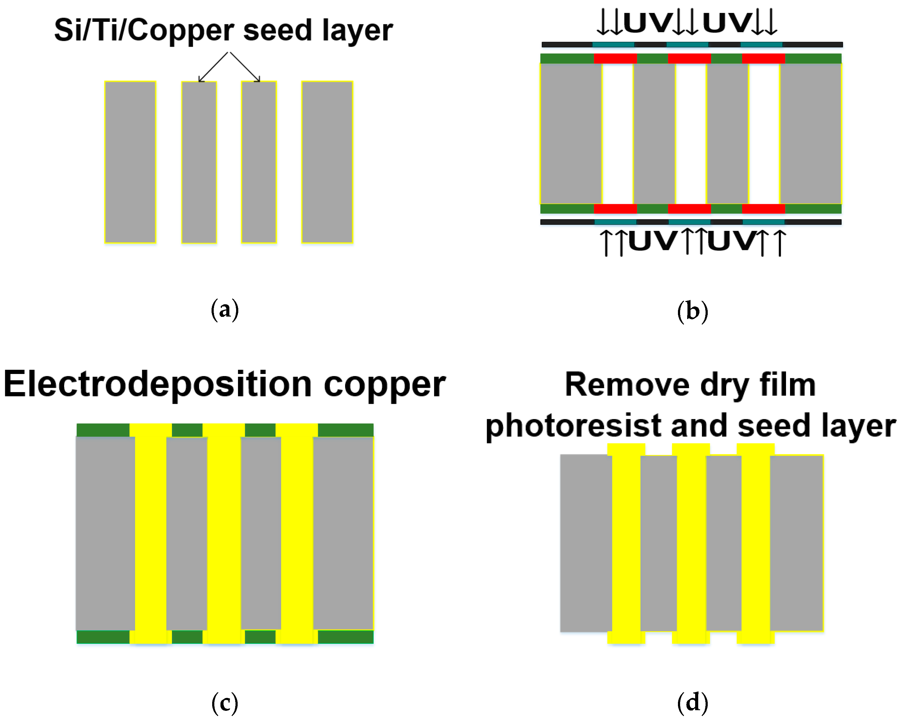
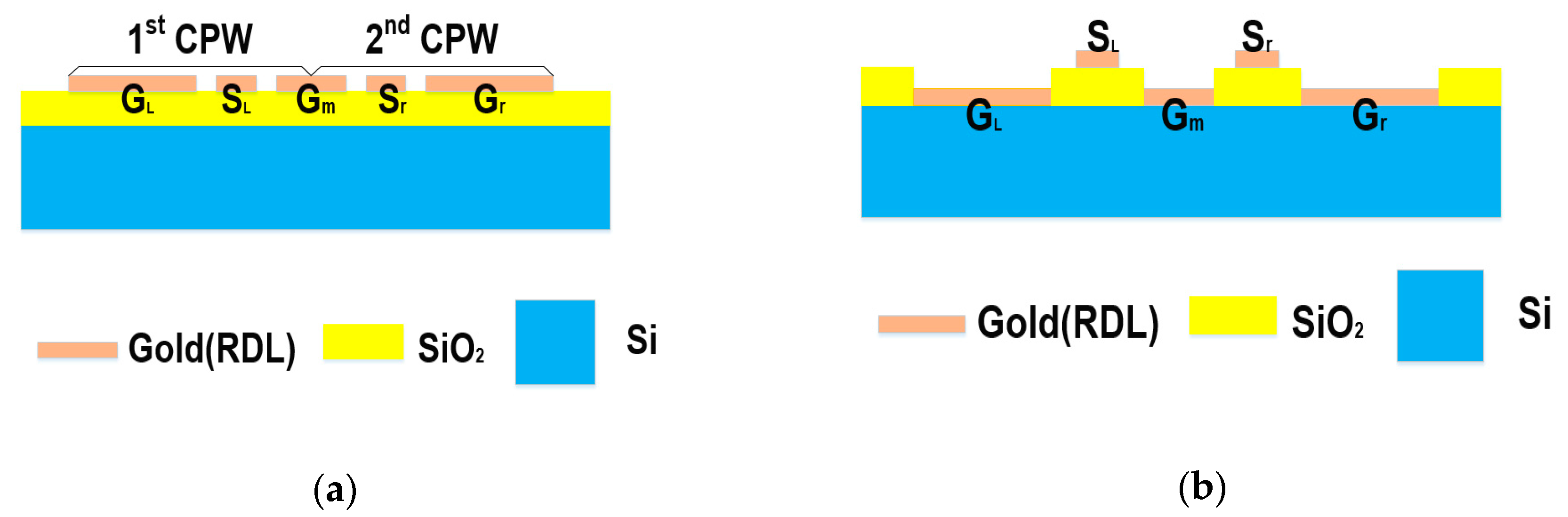
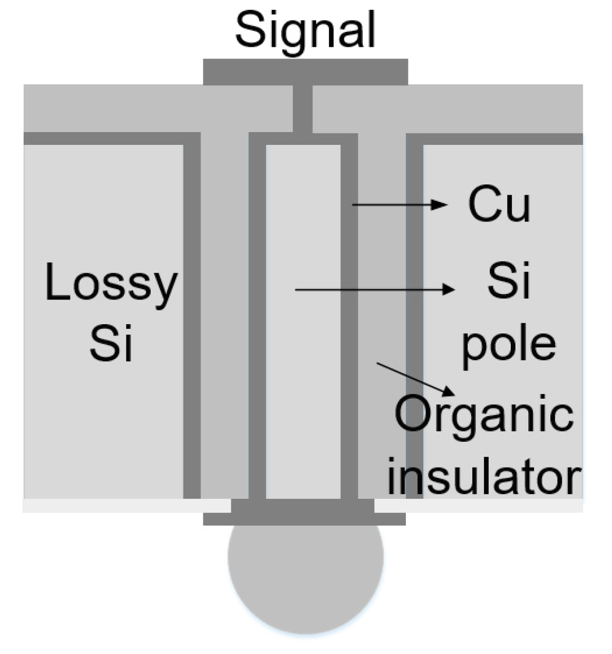
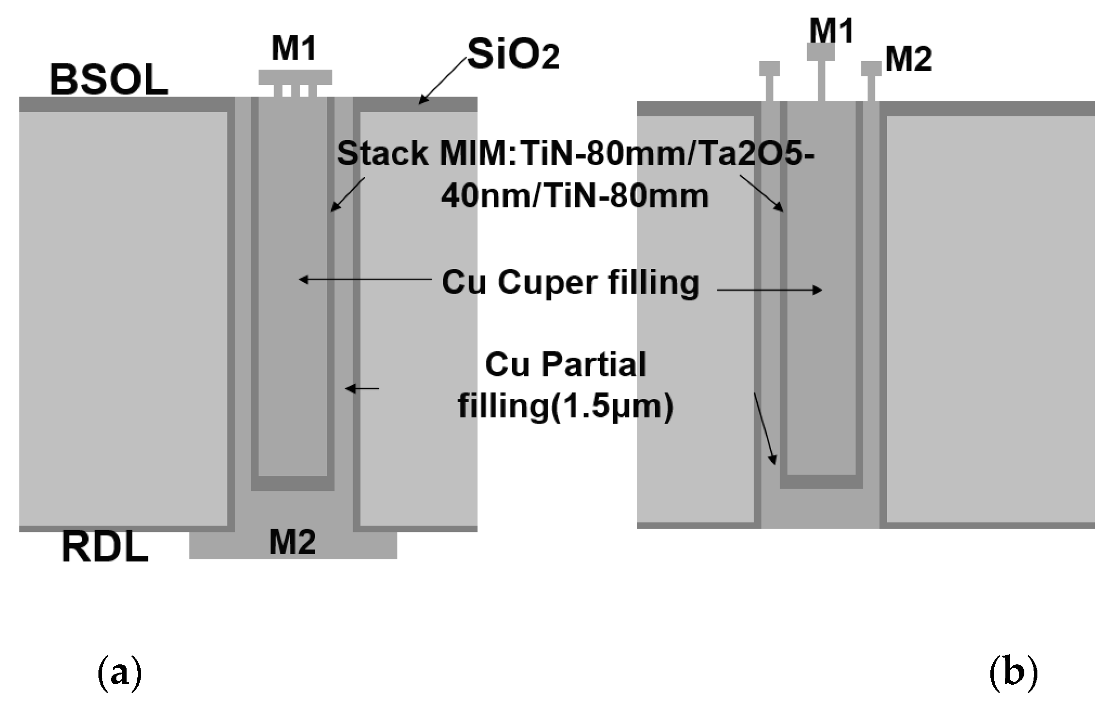
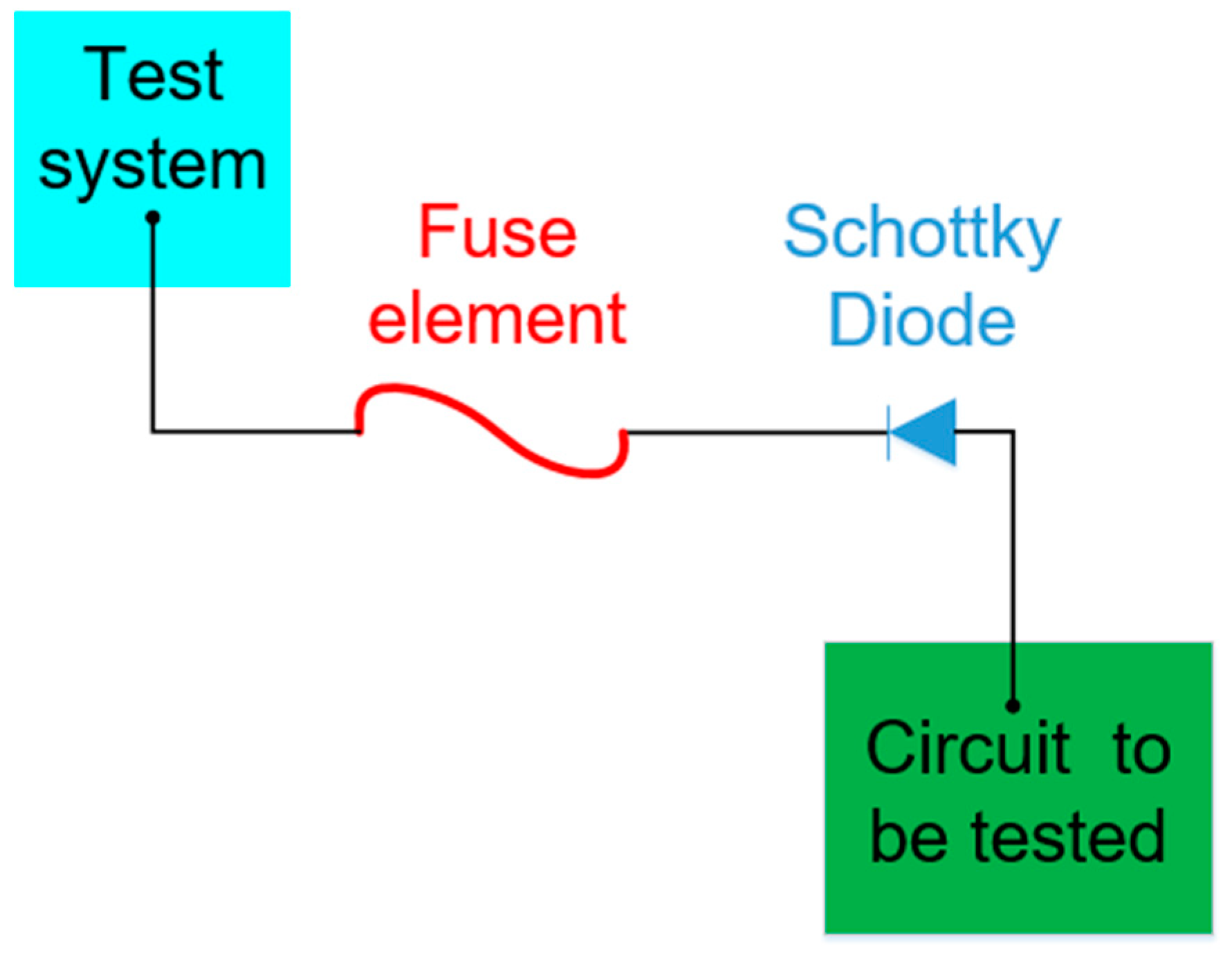
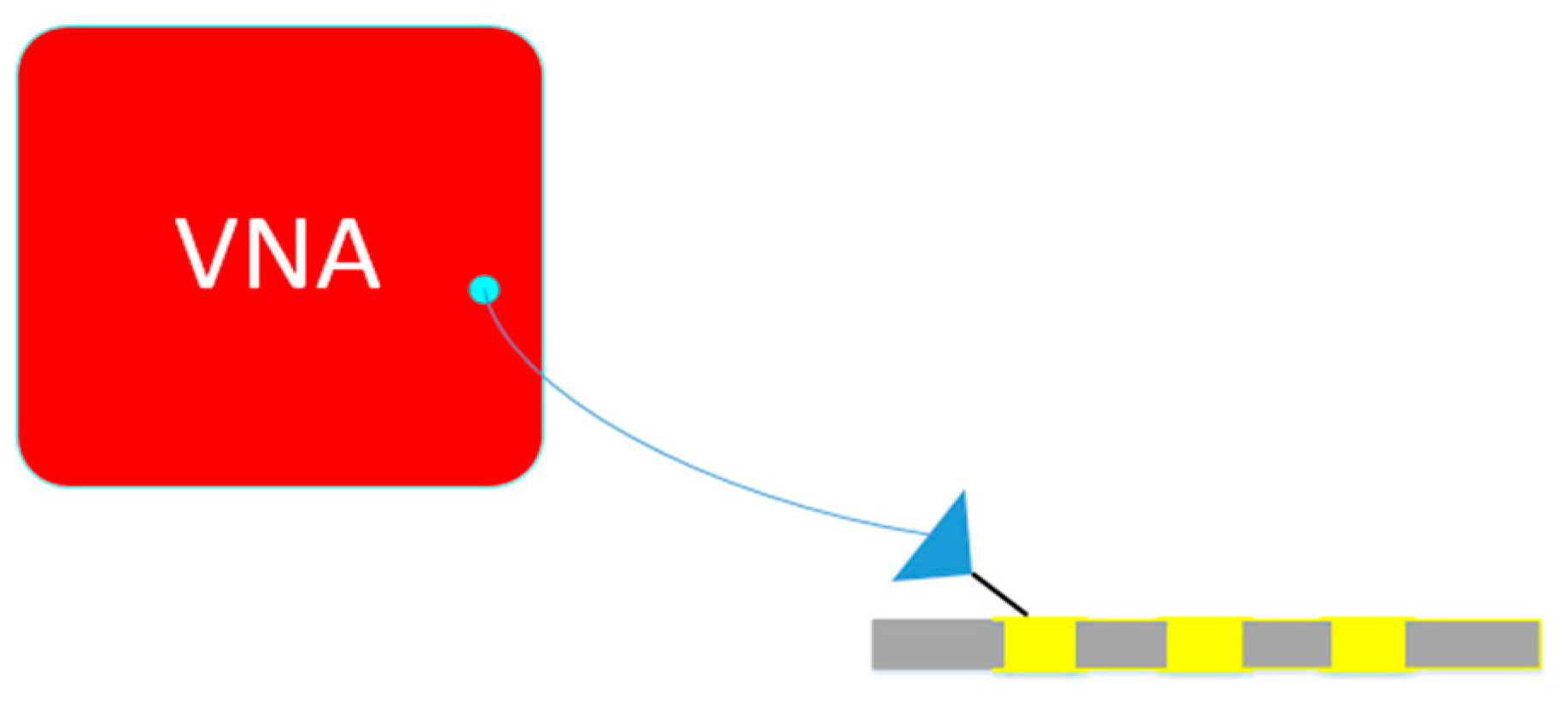
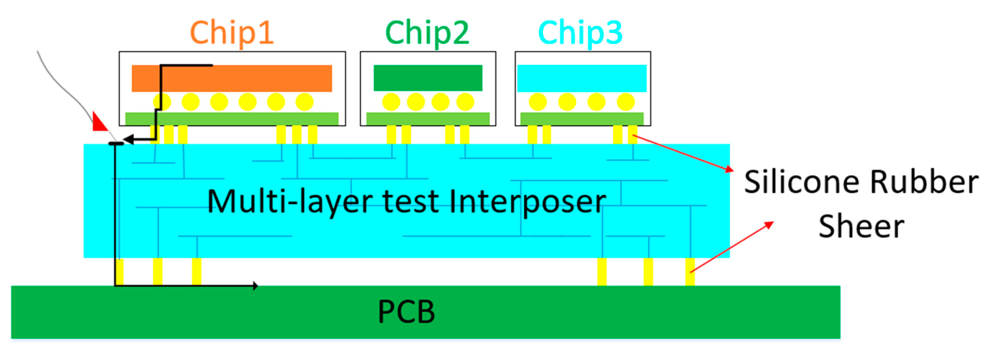
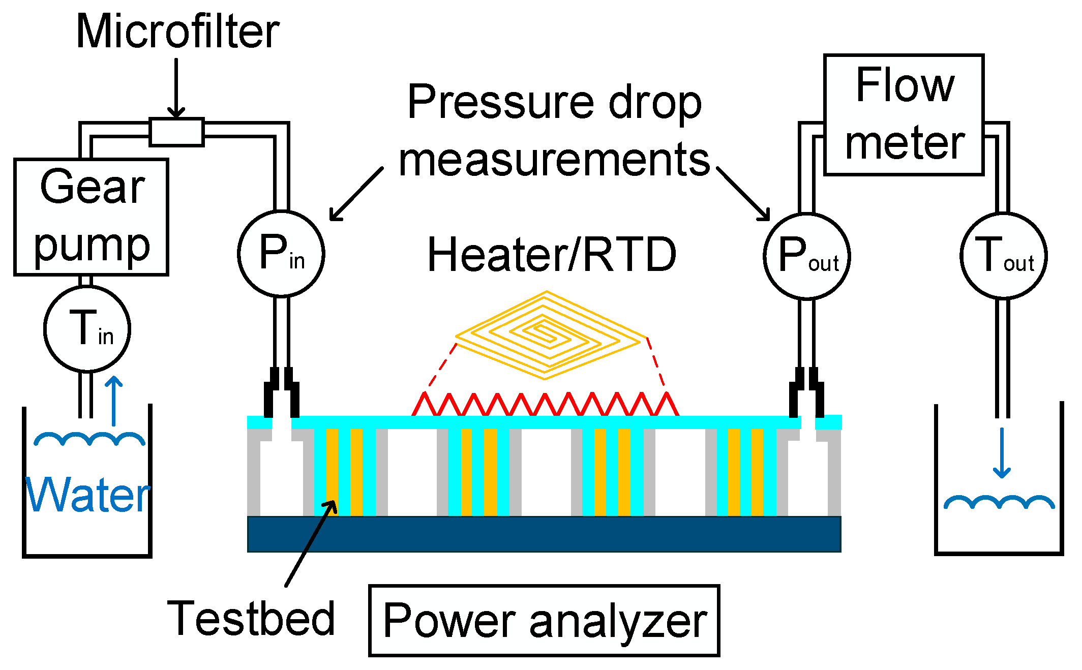
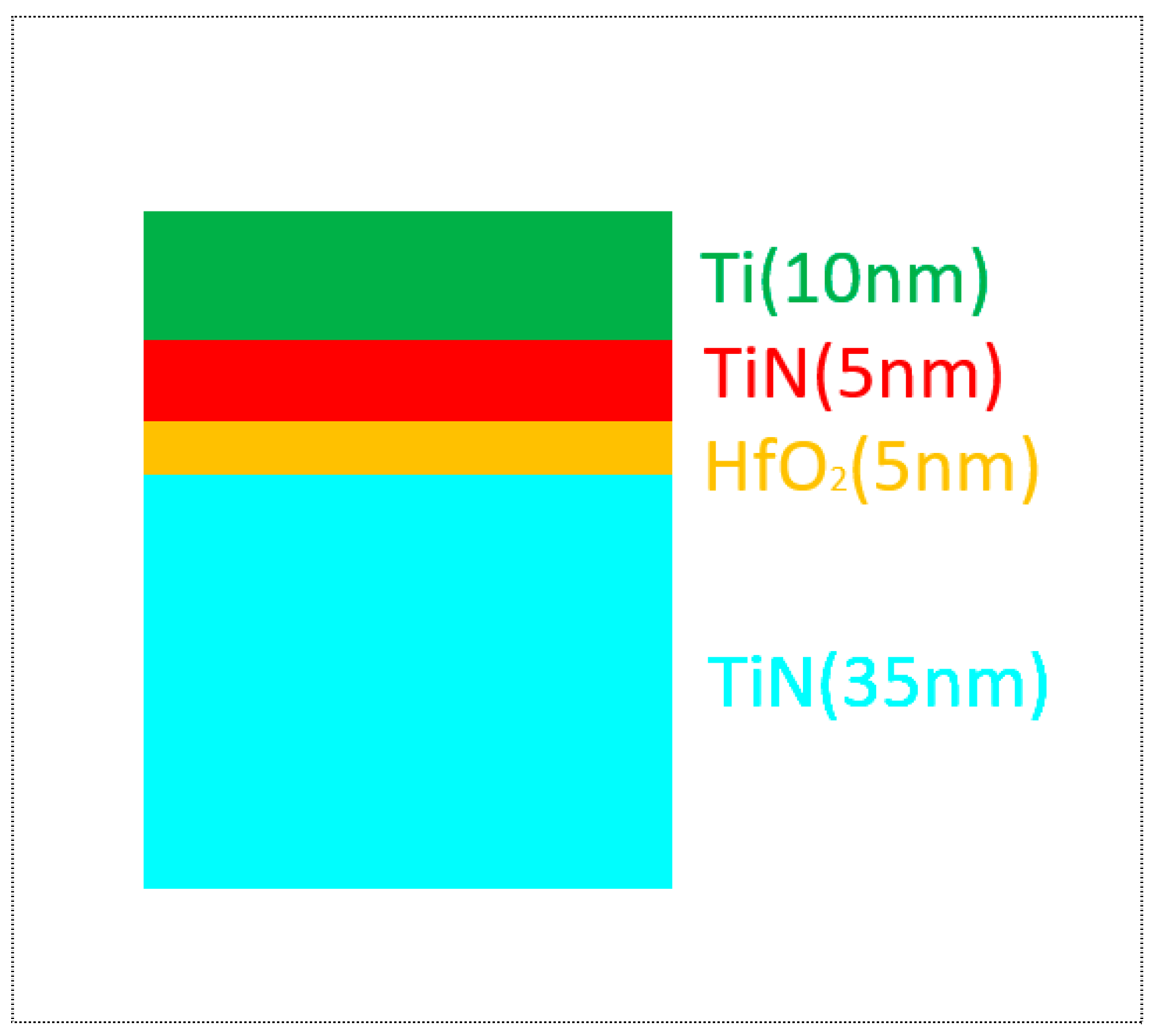
Table 1.
Summary of methods to metallize TSVs.
| Application | Via Depth/Diameter | Cost | Performance | Reference |
|---|---|---|---|---|
| 3D ASIC and memory integration | 220/50 μm | High | A total of 3000 cycles with 10 min ramps and dwell from 0 to 100 °C | [14] |
| Passive Interposer | 230/80 μm | Low | High density | [15] |
| RF wireless devices | 120/60 μm | N/A | The loss of 0.6 dB/mm at 60 GHz. | [22] |
| Passive Interposer | 130/50 μm | N/A | No electrical failure occurred in all samples after 500 MSTs (moisture sensitivity testing) and 1000 TCTs (thermal cycling testing from −40 °C to 125 °C). Only two of them failed after 3000 TCTs. | [24] |
| On-silicon-interposer | N/A | N/A | Four times higher than the data rate of HBM generation 2 | [26] |
| 3D integration | 100/40 μm | Lower | Simplified the integrated process flows, enhanced the reliability | [27] |
| high-density RDLs of silicon interposers | -/10 μm | Lower | reduce the amount of waste materials | [28] |
Table 2.
Summary of materials to metallize TSVs.
| Mechanism/Material | Via Depth/Diameter | Duration | Reference |
|---|---|---|---|
| Cu | 100/10 μm | Coverage of near 100% and lower leakage current | [29] |
| Vacuum pressure/Molten 1SAC305 solder | 220/30 μm | The filling time is 4 s; The wetting layer deposition may take more than 1 h. | [30] |
| RF-MEMS switch/Molten Sn-Ag solder | 300/150 μm | The wetting layer deposition may take more than 1 h. | [31] |
| N2 gas pressure/Molten Zn-Sn alloy | 150/50 μm | The wetting layer deposition and Zn electroplating may take more than 3 h. | [32] |
| Inkjet printer/Ag-based ink | 115/80 μm | N/A | [33] |
| Very high aspect ratio TSVs/Gold | 625/30 μm | Adapt standard wire bonding technology to fill the through via holes | [34] |
| 3-D integration/Ag-based conductive polymers | 500/150 μm | The resistance is between 30 and 55 Ω | [35] |
1 Sn 96.5%\Ag 3.0%\Cu 0.5%.
Table 3.
Summary of 3D PICS structures.
| Waveguides Material | Waveguides Thickness | Performance | Reference |
|---|---|---|---|
| Si | 500 nm | Promoting light coupling to other materials for efficient electro-optical modulation | [54] |
| Si | 220 μm | Negligible loss | [55] |
| SiN | 100 μm | power variation less than 0.1 dB | [56] |
Table 4.
The TSV and interposer technology summary.
| Classification | Research Content | Conclusion | Reference |
|---|---|---|---|
| The interposer production | A passive silicon interposer | Cost and performance-effective. | [14] |
| The interposer production | A passive silicon interposer | High density and low-cost. | [15] |
| The interposer production | A passive silicon interposer with annular TSVs. | The loss of 0.6 dB/mm at 60 GHz. | [22] |
| The interposer production | An annular copper through-silicon via (TSV) integration process. | No electrical failure occurred in all samples after 500 MSTs. | [24] |
| The interposer production | A new on-silicon-interposer passive equalizer for HBM. | Higher performance. | [26] |
| The interposer production | Through-hole filled with micro-bump integration production. | Simplify the production process, save costs and enhance its reliability. | [27] |
| The interposer production | Redistribution layers were fabricated using Combination of E-Jet and Inkjet Printing. | Simplify the production process and save costs. | [28] |
| The interposer production | TSVs filled with void-free copper. | Nearly 100% coverage and lower leakage current. | [29] |
| The interposer production | TSVs filled with the molten solder. | The 100% filling ratio for vias. | [30] |
| The interposer production | A radio frequency MEMS. | Short filling time. | [31] |
| The interposer production | Fill vias with the Sn Zn. | Higher performance. | [32] |
| The interposer production | Print blind vias using an inkjet printer. | Avoid the filling material melting process. | [33] |
| The interposer production | A new concept for the quick metallization of TSVs. | Super high aspect ratio. | [34] |
| The interposer production | Ag-based and C-based conductive polymers. | Accelerate the metallization process and enhance the electrical connection quality. | [35] |
| The interposer production | High-resistance silicon instead of p-type low-resistance silicon as a Interposer material. | High-resistance -silicon interposer can be well suited to high-frequency circuits. | [36] |
| The interposer production | Glass interposer instead of Silicon interposer. | Reduce costs. | [37] |
| The interposer production | TSV vias filled with Cu metal are converted to fill with polysilicon for use in MEMS devices. | It is more compatible with high temperature process, without metal, and suitable for the special requirements of MEMS technology | [38] |
| The interposer production | Nano-carbon filled glass adapter plate | Reduce the maximum temperature of the interposer in a large extent. | [39] |
| The interposer structure | Ohm contact CPW RDL structure with ground directly in contact with the silicon substrate | Reduce signal crosstalk to some extent. | [44] |
| The interposer structure | The silicon-interposer structure composed of a thin metal substrate | The far-end crosstalk can be reduced to a certain degree when the center distance of the via hole is greater than or equal to the thickness of the silicon substrate. | [45] |
| The interposer structure | A novel silicon-core coaxial TSV structure. | The structure has the characteristics of low loss, high performance and simple production process. | [46] |
| The interposer structure (TSC) | Integrate 3D deep on silicon interposer. | Increase the capacitance density and improve the chip package performance. | [47] |
| The interposer structure (TSC) | Production of axial TSC and radial TSC. | The using of radial TSC can reduce the ESL and increase the SER. | [48] |
| The interposer structure (3D PICs) | Efficient electro-optical modulation. | Promote light coupling to other materials. | [54] |
| The interposer structure (3D PICs) | 220 nm-thick silicon waveguides. | With negligible loss. | [55] |
| The interposer structure (3D PICs) | A high-density wafer-scale 3-D silicon-photonic integrated circuits. | Lower power variation. | [56] |
| The interposer testing | E-fuse, a new test framework, was proposed based on the plug-in structure of integrated circuit test. | Connect the test system and the circuit to be tested and separated. | [61] |
| The interposer testing | Propose a novel de-embedding methodology and broadband microprobe measurement | There is a transition to resistance around 1 GHz due to the property of the silicon substrate, and then dominated by capacitive behavior when frequency goes up to 4 GHz | [65] |
| The interposer testing | Designed a test interposer for POP | Signal integrity issues can be tested without contact with solder joints, reducing errors due to the solder-joints damage and the poor contact | [66] |
| The interposer thermal design | Designed and fabricated a silicon interposer embedded with microfluidic channels. | Thermal conductivity increased significantly. | [67] |
| The interposer thermal design | 3-D embedding concept of optical and electrical dies. | Address the thermal issues based on wet-etched silicon interposer with low cost | [70] |
| The interposer thermal design | Wet-etched three-level Silicon Interposer | Only a 0.1and 0.8-dB additional penalty. | [71] |
| Micro-bump | Micro-bump failure | Sensitive to the loading mode | [75] |
| Micro-bump | Examine the reliability of Ni/Sn3.5Ag (15 μm)/Ni micro-bumps. | The orientation affects the electromigration reliability. | [81] |
| Micro-bump | Power one daisy chain of the micro-bumps. | The latter failed due to thermomigration | [82] |
| Micro-bump | The thermo-mechanical properties of SnAg micro-bumps | Significantly weaken its mechanical and electrical properties. | [87] |
Table 5.
Characteristics of the studied Schottky diodes.
| Part Number | Technology | Active Area | CMOS | Reference |
|---|---|---|---|---|
| MSO9104A | PPL | N/A | 130 nm | [107] |
| N/A | HBT | N/A | N/A | [110] |
| EPC2019ENG | GaN | N/A | N/A | [111] |
| 3DG110 | BJT | N/A | N/A | [114] |
| STPSC1006D | SiC Schottky diodes | 2.31 mm2 | N/A | [121,122] |
| STPSC10H065DY | SiC Schottky diodes | 2.62 mm2 | N/A | [121,123] |
| FM22L16 | FRAM | N/A | 130 nm | [125] |
| MT29F128G08CBECBH6 | NAND | N/A | 16 nm | [128] |
| N/A | FinFET | N/A | 16 nm | [52] |
| Artix-7 | SRAM-FPGA | N/A | 28 nm | [53] |
Table 6.
Characteristics of the used ion beams.
| ION | ENERGY (MeV) | Material | LET (MeV/(mg/cm2))/Tilt (°) | Projected Range (μm) | Facility | Reference |
|---|---|---|---|---|---|---|
| Kr | 480 | Si | 37.6 | N/A | HIRFL | [107] |
| Kr | 768 | SiC | 33.8/0 | 63 | RADEF | [121,122] |
| Fe | 523 | SiC | 20.1/0 | 64 | RADEF | [122] |
| Ar | 372 | SiC | 10.9/0; 11.7/30; 14.3/45; 15.7/50 | 78 | RADEF | [123] |
| N | 139 | Si | 1.8/0 | 202 | RADEF | [126] |
| Fe | 523 | Si | 18.5/0 | 97 | RADEF | [126] |
| Kr | 768 | Si | 32.1/0; 45.4/45 | 94 | RADEF | [126] |
| Ne | 186 | Si | 3.6/0; 4.2/30; 5.1/45 | 146 | RADEF | [126] |
| Xe | 1217 | Si | 60/0; 69.3/30; 84.8/45 | 89 | RADEF | [126] |
| Xe | 466 | Si | 64.3/0 | 37 | GANIL | [126] |
| Xe | 1790 | Si | 50.2/0 | 137 | GANIL | [126] |
| B | 108 | Si | 0.9/0 | 306 | BASE | [126] |
| Ne | 216 | Si | 3.5/0 | 175 | BASE | [126] |
| Si | 292 | Si | 6.1/0 | 142 | BASE | [126] |
| Ar | 400 | Si | 9.7/0 | 130 | BASE | [128] |
| Cu | 659 | Si | 21.2/0 | 108 | BASE | [128] |
| Xe | 1232 | Si | 49.3/0 | 148 | BASE | [128] |
| C | 50 | Si | 3/0; 5.21/45; 9.13/60 | N/A | 1LAFN-USP | [130] |
1LAFN-USP: Laboratório Aberto de Física Nuclear of the Universidade de São Paulo
Table 7.
The impact of high-energy heavy ions on semiconductor device research.
| Object/Methods | Content | Conclusion | Reference |
|---|---|---|---|
| SiO2/The high-energy heavy ions radiation simulator | Deduced the dependence of breakdown voltage on the deposition energy. | The breakdown voltage is a linear function of the residual charge after ion orbital recombination | [99,100] |
| PLL/HIRFL | The radiation hardening of PLL (low-jitter phase-locked loop) | The SEE of hardened PLL are an order of magnitude higher than unhardened one | [107] |
| SiGe HBT/TCAD | The SEE caused by heavy ions and lasers in SiGe HBT | There is a moderately high LET threshold for heavy ion radiation changing the decay mechanism observed in SiGe HBTs from exponential to fast exponential decay with significant diffusion tail | [110] |
| GaN/TCAD | The SEE of GaN transistors after heavy-ion radiation | The self-polarization of the gate caused by the hole current originating from the ion beam leads to a momentary turn-on of the device. | [111] |
| NPN transistor/EN Tandem Accelerator | The defect characteristics of the displacement caused by the irradiation of various heavy ions in an NPN transistor | The degradation of device electrical performance is NIEL independent. | [114] |
| SiC Schottky power diodes/TCAD | The charge transport mechanism (current-voltage characteristics) of heavy-ion-causing damages in SiC structures. | The charge transport is controlled by space-limited charge flow | [121] |
| SiC Schottky power diodes/TCAD | The SEB of SiC Schottky power diodes caused by the heavy ion. | The increment of the reverse leakage current induced by the heavy ion in the SiC-based device is caused by the synergistic effect of the energy deposition of the ions and the bias voltage. | [122] |
| SiC Schottky power diodes/TCAD | The dependence of heavy ion-induced degradation on the incident angle and energy deposition in SiC Schottky diodes. | The heavy ion-induced degradation in SiC Schottky diodes is strongly dependent on incident angle. | [123] |
| FRAMs/RADEF& GANIL | The effect of heavy ion on commercial FRAMs | The static flip-up cross section in FRAM devices is very low due to the intrinsic radiation hardness of the ferroelectric layer-based memory cells. | [126] |
| 16 nm NAND flash/BASE | The SEE of a Micron 16 nm NAND flash | The SEU cross-section is inversely proportional to the cumulative effect which in turn leads to unsteady rollover rates and contrary to the traditional assumption. | [128] |
| 16 nm FinFET/TCAD | The effects of heavy ion impact angles on the SEE of a 16-nm FinFET 3D TCAD model D-latch. | The probability of failure and the SEU cross-section increase with the increase of the tilt angle, but will decrease with the increase of the angle when heavy LET heavy ions are incident. | [129] |
| 28 nm SRAM/SRIM | The effect of the incidence and rotation angle of heavy LET ions on the MBU effect of an FPGA based on 28 nm SRAM. | The MUSCA SEP tool was used to highlight the angular configuration as a function of memory cell layout strongly influences sensitivity of CRAM and BRAM in FPGA Artix-7. | [130] |
Table 8.
Existing heavy ion accelerators.
| Heavy Ion Accelerator Name | Conversion from Gaussian and CGS EMU to SI Accelerators | The Type of Particles Provided | The Energy of Particles Provided | Reference |
|---|---|---|---|---|
| HI-13 | Chinese Department of Nuclear Physics. | H~F, Al~Cl, Ca, Ag, Ti, Fe, Cu, Ge, Br, Nb, I, Hf, Au | ~100 MeV/u | [131] |
| HIRFL | Chinese National Laboratory of Heavy Ion Accelerator of Lanzhou. | C~Ta | 1.22 MeV/u (238U72+) ~ 1100 (12C6+) MeV/u | [107] |
| BNL-RHIC | Brookhaven National Laboratory in the United States. | Proton ~ Au | ~100 GeV(Au) | [140,142] |
| BASE | Lawrence Berkeley National Laboratory in the United States. | B, Ne, Si, Ar, Cu, Xe et al. | ~10 MeV/ u(electron) | [128] |
| RADEF | Jyväskylä in Finland. | N, Fe, Kr, Ne, Ar, Xe et al. | ~1217 MeV/u (Xe) | [126] |
| GANIL | The University of Caen in France. | Xe, Kr et al. | 466/1217/1790 MeV/u (Xe)768 MeV/u (Kr) | [126] |
| RIKEN-RIBF | Japan’s RIKEN | Proton ~ U | 440 MeV/u(Light ions) 350 MeV/u (Heavy ions) | [142,143] |
| 8UD | São Paulo | 12C, 16O, 28Si, 35Cl, 63Cu | ~32 MeV/u | [144] |
Table 9.
Heavy ion accelerators under construction.
| Heavy Ion Accelerator Name | Country & Affiliation | The Type of Particles Provided | The Energy of Particles Provided | Reference |
|---|---|---|---|---|
| FAIR | German heavy ion research center GSI. | Proton ~ U | ~9.7 GeV/u (238U28+) | [137,139] |
| HIAF | Institute of modern physics, Chinese Academy | Proton ~ U | ~100 MeV/u (238U34) | [128] |
© 2018 by the authors. Licensee MDPI, Basel, Switzerland. This article is an open access article distributed under the terms and conditions of the Creative Commons Attribution (CC BY) license (http://creativecommons.org/licenses/by/4.0/).
Share and Cite
MDPI and ACS Style
Tian, W.; Ma, T.; Liu, X. TSV Technology and High-Energy Heavy Ions Radiation Impact Review. Electronics 2018, 7, 112. https://doi.org/10.3390/electronics7070112
AMA Style
Tian W, Ma T, Liu X. TSV Technology and High-Energy Heavy Ions Radiation Impact Review. Electronics. 2018; 7(7):112. https://doi.org/10.3390/electronics7070112
Chicago/Turabian StyleTian, Wenchao, Tianran Ma, and Xiaohan Liu. 2018. "TSV Technology and High-Energy Heavy Ions Radiation Impact Review" Electronics 7, no. 7: 112. https://doi.org/10.3390/electronics7070112
Note that from the first issue of 2016, this journal uses article numbers instead of page numbers. See further details here.