1. Introduction
Force Sensing Resistors (FSRs) offer versatile and cost-effective force readings to applications with space and weight constraints. FSRs can be fashioned into multiple shapes and dimensions to fulfill the requirements of a given final application [
1,
2,
3]; this can be done by simply cutting the nanocomposite film after the production process is done, followed by electrode positioning and wiring to assemble the final force sensor [
4]. The nanocomposite film is obtained by randomly dispersing conductive particles in an insulating polymer matrix [
5,
6,
7]. Finally, when the sensor is assembled, a time-multiplexed circuit is employed to read out the sensor’s resistance and provide a pressure profile map [
4,
8].
Nonetheless, FSRs have found limited acceptance in applications demanding accurate force readings due to the poor reproducibility of the piezoresistive behavior [
9,
10]. By taking a glance at the datasheets of commercial FSRs [
11,
12,
13], they exhibit from ten to one hundred times more drift and hysteresis error than load cells. Fortunately, a great effort is currently placed on improving the performance of FSRs by investigating multiple trends such as the integration of carbon nanotubes in the polymer matrix [
7,
14], changing the electrode configuration of the assembled sensor [
15,
16], testing different types of polymers [
17,
18], and adding non-conductive nanoparticles to reinforce the polymer matrix with the aim of reducing creep [
9].
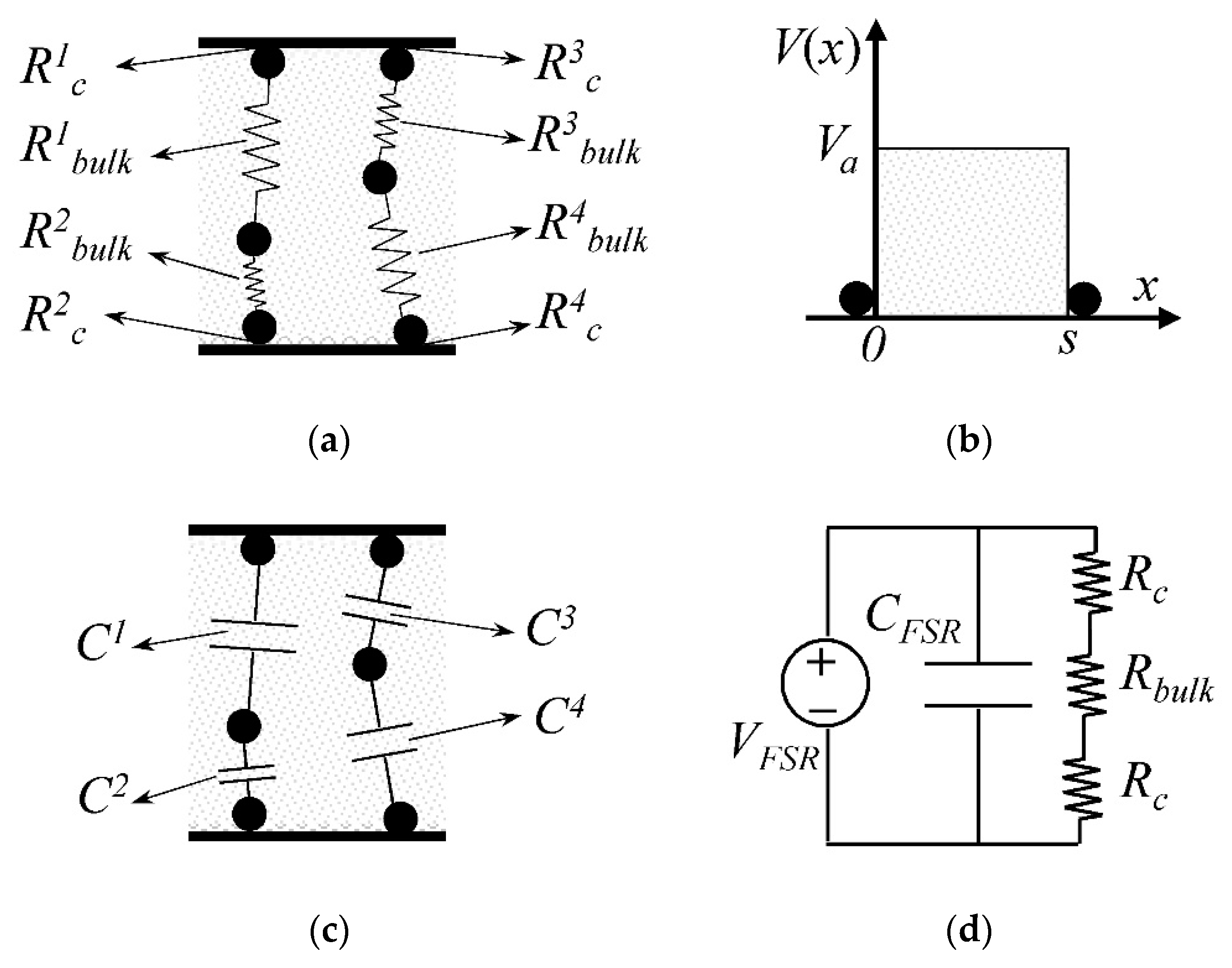
On the other hand, previous authors’ works have focused on a completely different approach to improve the accuracy of FSRs. The authors have developed a physical model for the quantum tunneling conduction of FSRs that comprises the series connection between multiple tunneling resistances (
Ribulk) and contact resistances (
Ric) [
19]; this is depicted in the sketch of
Figure 1a. The tunneling resistance takes place at the tunneling path of two particles separated by a potential barrier of width
s and height
Va, where
s is also known in the literature as the mean inter-particle separation. The polymer matrix acts as the insulating potential barrier in the nanocomposite; this is shown in
Figure 1b.
The contact resistance takes place between the sensor electrodes and the conductive particles, and between neighboring particles, but for simplicity, the sketch from
Figure 1a only shows the former scenario. The particles shown in
Figure 1a may be formed by nanoparticle agglomerates that behave as greater-microscopic-particles. These neighboring nanoparticles also exhibit contact resistance among them.
Both resistances,
Ribulk and
Ric, are stress-dependent but only
Ribulk is modified by the driving voltage (
VFSR). A detailed discussion on the tunneling resistance,
Ribulk, is later addressed in
Section 2.1 Conversely, the contact resistance,
Ric, only depends on the physical constriction occurring at the interface between two materials, and therefore,
Ric is voltage-independent. Computer simulations and experimental results have demonstrated the validity of the authors’ model in that it is able to predict a lower drift error for incremental values of
VFSR [
20]. This implies that the drift error can be minimized by trimming
VFSR in the driving circuit. Note that this is opposed to what the manufacturers of FSRs have stated in their product datasheets [
11,
12,
13], i.e., a constant drift error regardless of
VFSR.
Following the authors’ model, the distributed capacitance can be found along the multiple tunneling paths of the nanocomposite; see
Figure 1c. The total capacitance of an FSR can be computed from the multiple lumped capacitances (
Ci) which are connected in series and in parallel. Similarly, the total resistance of an FSR (
RFSR) can be computed from the series and parallel connections of
Ric and
Ribulk, thus yielding
Rc, and
Rbulk; see
Figure 1d. Previous authors’ works have demonstrated that performing capacitance readings on FSRs yield a lower hysteresis error [
21,
22], this has been experimentally measured and also predicted by theoretical models which are later addressed in
Section 2.3.
The development of a physical model for the current conduction of FSRs is of paramount importance for the definition of strategies that enhance the accuracy of such devices; this can be done in a two-folded strategy. From the standpoint of a nanocomposite designer, the physical model provides a full overview of the design parameters that impact the FSRs’ performance the most. For instance, it may be interesting to simulate—prior to assembly—the influence of choosing carbon black or metallic particles as the nanocomposite filler. Multiple simulations can be performed with a wide range of design parameters, such as the mass ratio of nanoparticles to polymer, the type of polymer, the particles’ dimensions and shape, etc. From the standpoint of a final user, the physical model aims to design the most appropriate driving circuit that maximizes the sensors’ performance. Based on the latter statement, the target of this study is to design and test a driving circuit that minimizes—or even removes—most of the error sources of FSRs, where drift, hysteresis, and sensitivity degradation are the most important error sources.
The rest of this paper is organized as follows:
Section 2 reviews the physical model, the error sources and the types of error in FSRs. A detailed design of the self-compensated driving circuit is presented in
Section 3, followed by the experimental setup, results, and discussion in
Section 4. Conclusions are stated in
Section 5. With the aim of obtaining representative results, the experimental data from this study were collected from eight FlexiForce A201-25 sensors (Tekscan, Inc., Boston, MA, USA) manufactured from an elastomeric polymer, as the insulating phase, and carbon black nanoparticles as the conductive phase [
23,
24].
2. Review of the Underlying Physics and Important Definitions of FSRs
The authors’ proposed model and experimental data from our previous works are presented here [
19,
20]. The authors’ proposed model imposes a voltage-dependent behavior for the tunneling conduction of FSRs; this is radically different from well-known models in the literature [
6,
25,
26]. The authors’ proposed model has demonstrated its validity by predicting-up to some extent-the sensitivity degradation of Conductive Polymer Composites. Additionally, it predicts that the drift error is voltage-dependent, just as experimentally measured [
19,
20].
The main sensing mechanism of FSRs is the reduction of the mean inter-particle separation,
s, when subjected to mechanical stress (
σ), i.e.,
s is a stress-dependent function defined from
where
M is the compressive modulus of the nanocomposite and
s0 is the inter-particle separation when
σ = 0. For incremental values of stress,
s is proportionally reduced, but the tunneling resistance exhibits a dramatic decrement due to the non-linear behavior of quantum tunneling. The authors have demonstrated that additional factors have influence on the resistance changes; these are the contact resistance,
Rc, and the effective area for tunneling conduction (
A) [
19]. They are briefly described ahead.
2.1. Physical Model for Quantum Tunneling Conduction of FSRs
From
Figure 1d, the total resistance of an FSR can be computed from
If the FSR is sourced with a constant
VFSR, the voltage drop across the tunneling barrier (
Vbulk) can be found from sensor current (
I) and Equation (2) as
In 1963, Simmons derived a set of piecewise equations for the quantum tunneling conduction through thin insulating films [
27]. The piecewise intervals are defined as a function of
Vbulk. The Simmons’ equations can be arranged to estimate
Rbulk. However, an analytic solution for
Rbulk is only possible when
Vbulk ≈ 0. For larger values of
Vbulk, only a numerical value can be found for
Rbulk. The expressions relating
Vbulk with
I are presented next.
If
Vbulk >
Va/
e
where
m and
e are the electron mass and charge, respectively, and
h is the Planck constant. The effective area for tunneling conduction,
A, is a stress-dependent magnitude with experimentally-determined parameters
A0,
A1, and
A2 given by
In order to calculate Rbulk for Equations (5) and (6), it is necessary to replace Equation (3) and find a numerical solution. Then, the quotient Rbulk = Vbulk/I can be computed. This procedure is not necessary for the interval of Equation (4). Note that Equations (5) and (6) impose a voltage-dependent behavior for the tunneling resistance, and consequently, the resulting errors, hysteresis, and creep, also depend on VFSR; this is because the tunneling and the contact resistance have different dynamics as described next.
Mikrajuddin et al. [
28] and Shi et al. [
29] have found expressions for the constriction (contact) resistance that exists between electrodes of arbitrary sizes. In their work, the contact resistance follows power laws with fixed coefficients, but some modifications had to be introduced by the authors in order to account for the stress-dependent area of Equation (7). Finally, the contact resistance,
Rc, can be found from
where
Rpar is the net resistance of the conductive particles dispersed in the insulating polymer matrix and
R0c and
k are experimentally-measured parameters. The numerical value of the parameters
R0c,
k,
A0,
A1, and
A2 can be found in Reference [
19] for the FlexiForce A201-1 (Tekscan, Inc., Boston, MA, USA) and the Interlink FSR 402 sensors (Interlink Electronics, Inc., Westlake Village, CA, USA) with nominal ranges of 4.5 N and 20 N, respectively.
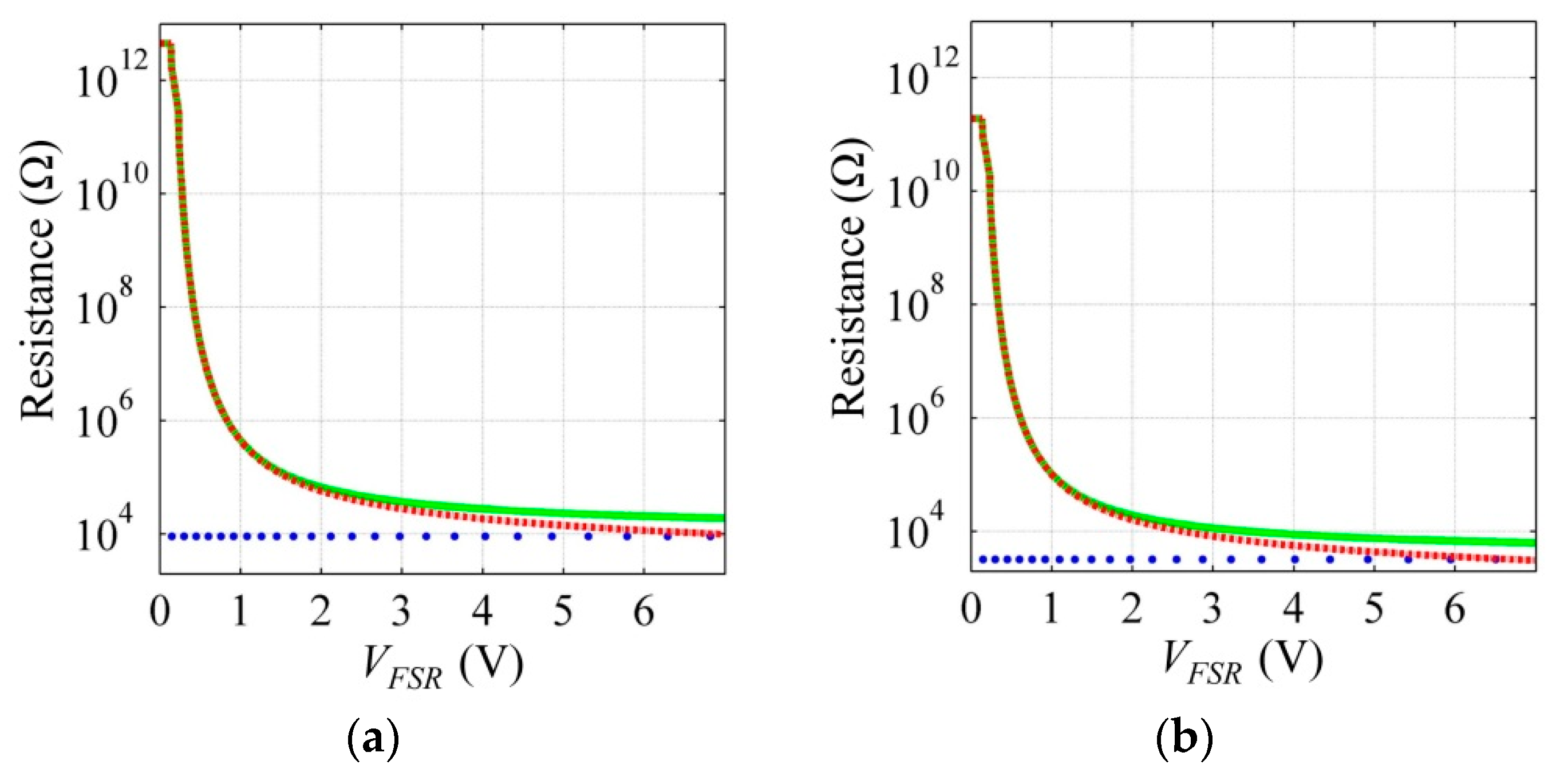
Figure 2 shows plots of
RFSR,
Rbulk, and
Rc as a function of
VFSR for two different mechanical loads. Note that
Rbulk dominates for low
VFSR, whereas at large
VFSR, the contact resistance dominates; so if
VFSR is chosen accordingly, the dynamic behavior of
Rbulk or
Rc can be independently studied.
It must be highlighted that the authors’ model can be applied to any FSR operating on the basis of quantum tunneling; this is because Equations (2)–(8) are stated in terms of universal constants (
m,
h,
e), and in terms of specific properties from the polymer and the conductive particles (
Va,
M). The inter-particle separation is defined by the mass ratio between the conductive and insulating phases; this ratio is known in the literature as the filler volume fraction (
ϕ) [
6,
25,
26]. In general, the larger
ϕ is, the more sensitive the sensor becomes, so the nominal range of an FSR can be trimmed by setting
ϕ during manufacturing. The FlexiForce A201-25 sensor, with a nominal range of 110 N, has been assembled with a lower
ϕ than the FlexiForce A201-1 which exhibits a nominal range of 4.5 N. Considering that both FlexiForce sensors are manufactured from the same materials, the overall shape of
Figure 2 is held, with the only difference being that the FlexiForce A201-25 is less sensitive to applied stress due to the lower
ϕ.
2.2. Physical Model for the Capacitance of FSRs.
The total capacitance of an FSR (
CFSR) can be computed from the series and parallel connections of the multiple lumped capacitances of
Figure 1c. By definition,
CFSR can be calculated from
where
ε0 and
εr are the vacuum and relative permittivities, respectively. The parameters
A and
s have the same meaning from
Section 2.1. The authors’ previous work has demonstrated that
CFSR is voltage independent [
30] as Equation (9) predicts.
2.3. Error Sources and Types of Error in FSRs
The main error source in FSRs is the viscoelastic response of the polymer matrix that causes hysteresis and creep in the inter-particle separation; this implies that
s must be redefined from Equation (1) as a time (
t) and stress-dependent function
s(
σ,
t). Several models are available in the literature for the viscoelasticity of polymers [
31]. Some authors such as Zhang et al. [
25] and Kalantari et al. [
26] have combined the Kelvin–Voigt rheological model with Equation (4) obtaining overall good results. However, experimental observations from the authors have demonstrated that the creep phenomenon can be more accurately modeled if the whole set of Simmons’ equations are combined with the Burgers model, i.e., by replacing
s(
σ,
t) in Equations (4)–(6). A detailed derivation of the authors’ model for creep is available in Reference [
20]. The model predicts a lower creep in sensor resistance,
RFSR, for incremental values of
VFSR. This can be understood from the fact that the only source of creep is the inter-particle separation, so if
VFSR is large enough, the dominant role of
Rc yields low creep because
Rc does not depend on
s, see Equation (8). Conversely, for low values of
VFSR, the tunneling resistance dominates, and therefore, a larger creep is predicted by the model because
Rbulk does depend on
s in an exponential fashion, see Equation (4).
When dealing with capacitance measurements over extended periods of time, polymer creep causes a reduction in the inter-particle separation that increases the sensor’s capacitance; see Equation (9). This implies that capacitance drift is always positive and independent of VFSR. In opposition, the creep in RFSR is always negative, i.e., the sensor’s resistance decreases over time. This is the key aspect for designing a self-compensated driving circuit.
It must be highlighted that lower drift is always measured in
CFSR than in
Rbulk for a given specimen; this can be demonstrated by a comparison between Equation (9) and the expressions for
Rbulk. For the sake of simplicity, only Equations (4) and (9) are compared here. Given a small reduction (
ε) in the inter-particle separation due to polymer creep at time
tf, so that
s(
σ,
tf) =
si −
ε, where
s(
σ,0) =
si, readers can verify the validity of the following inequality:
where
γ = 4π(2
mVa)
−1/2/
h.
The inequality of Equation (10) can be understood as follows: due to the polymer creep, a small decrement in the inter-particle separation,
ε, always produces a larger normalized variation in
Rbulk than in
CFSR due to the exponential term of Equation (4). The same conclusion can be stated for the other voltage intervals of Equations (5) and (6). Concerning the hysteresis error, a similar demonstration to Equation (10) has been presented by the authors in Reference [
22].
Besides creep and hysteresis, FSRs may exhibit sensitivity degradation when subjected to dynamic (cyclic) loading. Sensitivity degradation has been reported in multiple studies related to polymer nanocomposites. Some authors have reported it for custom-made stress [
32,
33] and strain sensors [
34], thus indicating that sensitivity degradation is not exclusive of FlexiForce sensors [
35,
36], but rather, a phenomenon related with the polymer composite itself. The authors have experimentally demonstrated that sensitivity degradation is a voltage-related phenomenon that only occurs when the contact resistance is the main sensing mechanism of the FSR, i.e., when
VFSR is large enough [
20]. Unfortunately, this explanation is not yet fully satisfactory because Equation (8) does not predict sensitivity degradation by itself. This implies that additional phenomena are occurring at a microscopic level that the authors’ model does not account for. Up to now, the underlying basis of sensitivity degradation remains undisclosed and only hypotheses for this phenomenon have been provided. For instance, Canavesse et al. hypothesized that sensitivity degradation is caused by hysteresis [
32]. A proven method to avoid sensitivity degradation is to set
VFSR as low as possible so that the main sensing mechanism of the FSRs is the variation of the inter-particle separation [
20].
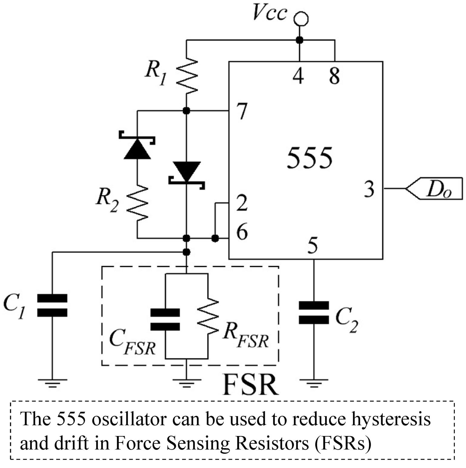
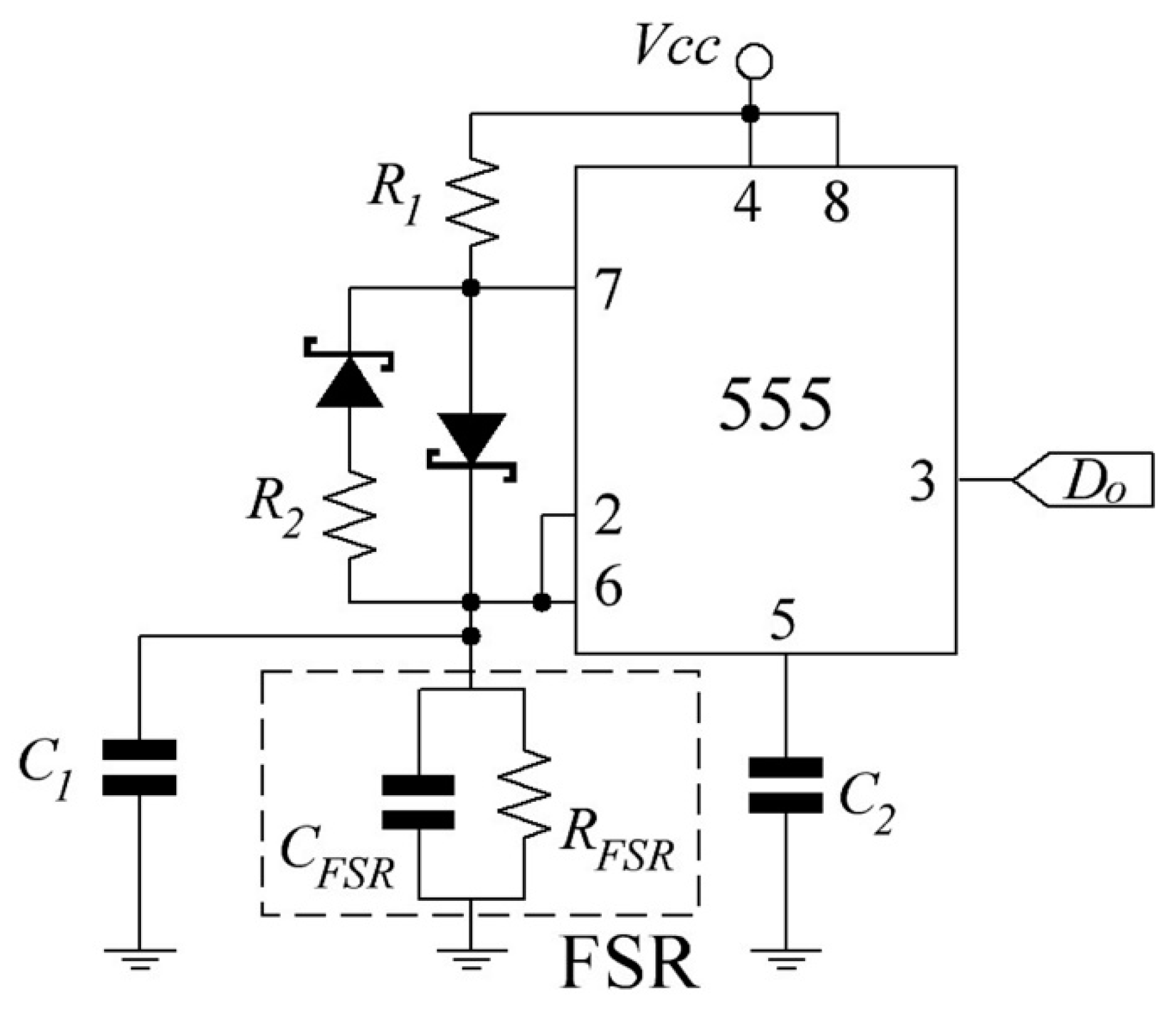
3. Design of a Self-Compensated Driving Circuit
When cyclic loading is applied to an FSR, sensitivity degradation and hysteresis are the main concerns, but when static loads are applied, drift is the main source of error. In order to design a self-compensated driving circuit, all these considerations must be taken into account.
The design methodology of this study gives the following importance order to the multiple types of error: first, sensitivity degradation, second, drift, and third, hysteresis.
With the aim of avoiding sensitivity degradation,
VFSR must be held as low as possible. The previous authors’ work has demonstrated that sensitivity degradation may appear even at voltages of 3 V [
20]. Unfortunately, there is not a universal threshold voltage for avoiding sensitivity degradation because conductive particles are randomly dispersed in the polymer matrix, and therefore, identical sensors do not exist. In order to minimize drift, the driving circuit must be designed so that capacitance creep is compensated by the resistance creep; this is not achievable in a straightforward manner as predicted by the inequality of Equation (10), so an offset is required to compensate for the larger creep in sensor’s resistance,
RFSR.
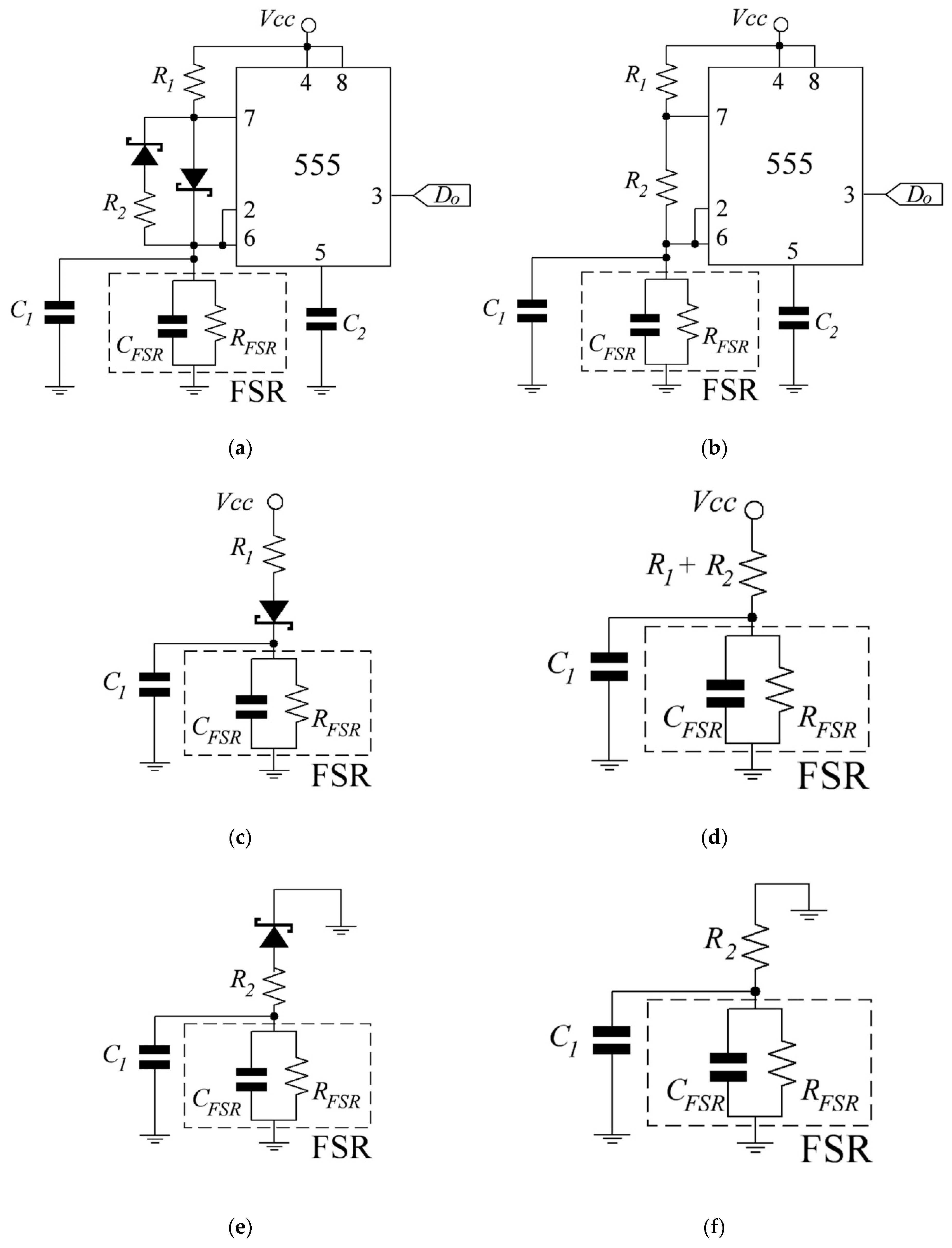
Based upon the previous statements, the driving circuit of
Figure 3 is proposed with
Vcc set to 2.5 V which is the lowest admissible supply voltage for the 555 device. In addition, the voltage across the FSR never goes beyond 2/3·
Vcc due to the operation principle of the 555. Given the low
Vcc, Shottky diodes should be used instead of regular diodes. The circuit output (
Do) is a square signal with frequency
f that changes accordingly with the applied stress. Measuring and correlating
f with the applied stress is the sensing mechanism of the circuit in
Figure 3. A comparison between the classical version of the astable oscillator and the circuit of
Figure 3 is addressed in
Appendix A.
The modified-astable 555 circuit in
Figure 3 imposes a time constant (
τ) of
τon =
Ce·
RFSR·
R1/(
R1 +
RFSR) for the charge phase, and
τoff =
Ce·
RFSR·
R2/(
R2 +
RFSR) for the discharge phase, where
Ce is given by
Ce =
C1 +
CFSR. The resistances
R1 and
R2 have the role of reducing the larger creep in
RFSR. Readers can verify that if
RFSR drifts to a certain amount, then
RFSR·
R1/(
R1 +
RFSR) and
RFSR·
R2/(
R2 +
RFSR) always creep less in the same time lapse. The resistances
R1 and
R2 are henceforth designated as the parallel-offset resistances. For instance, if
RFSR is heavily offset, it implies that the parallel connection between
R1 and
RFSR is dominated by
R1. Conversely, if
R1 and
RFSR are comparable, then
RFSR is slightly offset.
The optional capacitance
C1 has the role of lowering the oscillation frequency. As later demonstrated in
Section 4,
f results in the order of several hundred kilohertz which can be too high for some measuring circuits.
In order to understand how drift compensation is achieved, it is necessary to find expressions for the charge and discharge times of
Ce. The time required for
Ce to charge from 1/3·
Vcc to 2/3·
Vcc can be found from the expression
and the time required for
Ce to discharge from 2/3·
Vcc to 1/3·
Vcc is
However, Equation (11) can be further simplified with an admissible error by noticing that
RFSR is, in practice, many times larger than
R1, and thus,
RFSR/(
R1 +
RFSR) ≈ 1. This is later demonstrated in
Section 4. By replacing
RFSR/(
R1 +
RFSR) = 1 in Equation (11),
ton can be approximated to
3.1. Compensation Mechanism Using R1 = R2
In a first attempt—and for simplification purposes—the resistances
R1 and
R2 are set to be equal so that a single time constant is obtained for the charge and the discharge phases. Based on this assumption,
R1 =
R2, the time constant is given by
τ =
Re·
Ce, where
Re =
RFSR·
R1/(
R1 +
RFSR). From this observation,
ton and
toff are identical and the design criteria for drift compensation relies solely on the time constant as follows:
where
εR and
εC are the small variations in the sensor’s resistance and capacitance, respectively, due to creep in the inter-particle separation,
s(
σ,
t).
An explanation for the opposite signs of
εR and
εC was already presented in
Section 2.3 but it can be summarized as follows. The symbol “−
εR” is negative because the creep in
s(
σ,
t) yields a lower resistance just as Equation (2) and Equations (4)–(6) predict. The symbol “
εC” is positive because the creep in
s(
σ,
t) yields a larger capacitance as predicted by Equation (9). Finally, Equation (14) may be understood as follows: in order to compensate for the creep in
s(
σ,
t), the time constant of the circuit must remain unchanged; this can be achieved from the opposite creep characteristic of the sensor’s resistance and capacitance. If
R1 =
R2, the resulting frequency,
f, in
D0 can be approximately found from Equations (12) and (13) as next:
3.2. Compensation Mechanism Using R1 ≠ R2
A more accurate and general expression for
f can be found on the basis of first, setting different values for
R1 and
R2, and second, using Equations (11) and (12) for
ton and
toff as follows:
Nonetheless, Equation (16) is still an approximated expression because it does not take into consideration the voltage-dependent behavior of
RFSR; see
Figure 2 and Equations (4)–(6). For this reason, if
Vcc is changed in the circuit in
Figure 3, the resulting frequency is changed as well. This may seem to be a drawback of the authors’ proposed circuit, but it must be recalled that the manufacturer’s recommended circuit exhibits the same behavior in regard to
Vo measurements [
11].
If R1 and R2 are set different, the compensation mechanism is the same as that of Equation (14), but in this case, a degree of freedom is gained since R1 and R2 can be independently trimmed. The analytical calculation for the optimal values of R1 and R2 is challenging for two reasons: first, RFSR is voltage-dependent, and second, RFSR notably changes from one specimen to another. For these reasons, the optimal values of R1 and R2 were found in this study by following an empirical approach. It is later demonstrated that the design criteria from Equation (14) also minimizes the hysteresis in frequency readings.
4. Experimental Setup, Results, and Discussion
At this point, it must be highlighted that this study initially considered the usage of both FlexiForce and Interlink sensors. However, the Interlink sensors are manufactured using Non-Aligned Electrodes Element (NAEE) [
15]; the NAEE configuration uses interdigitated electrodes in opposition to the Traditional Sandwich Element (TSE) in
Figure 1a. The TSE configuration is employed by the FlexiForce sensors. The NAEE configuration avoids the formation of lumped capacitances, and thus, the Interlink sensors exhibited negligible and stress-independent
CFSR. For this reason, the Interlink sensors could not be tested with the circuit in
Figure 3.
The experimental setup comprised a tailored test bench for applying static and dynamic loads and two electrical circuits for collecting the sensors’ resistance and resulting frequency. A detailed description of the mechanical test bench has been presented by the authors in Reference [
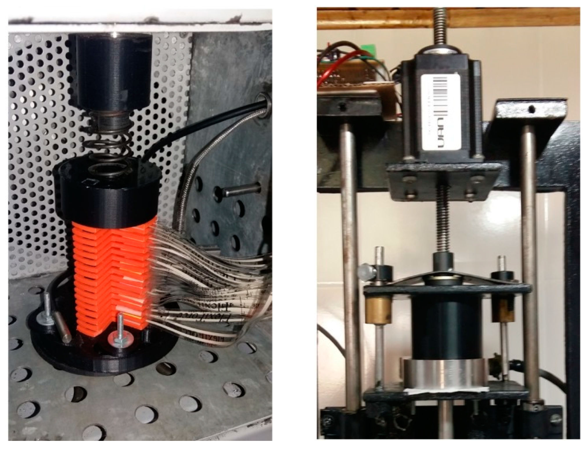
37], so only a brief description is next presented. The mechanical test bench is capable of handling multiple sensors using a sandwich-like configuration, see
Figure 4. Forces are applied through a linear motor with a load cell as a reference to close the force loops. The sensors’ holders have a notch on the upper side for avoiding the undesired displacement of the sensors, and a puck on the lower side for applying stress in an evenly distributed manner. The pucks are round with a diameter of 7.7 mm.
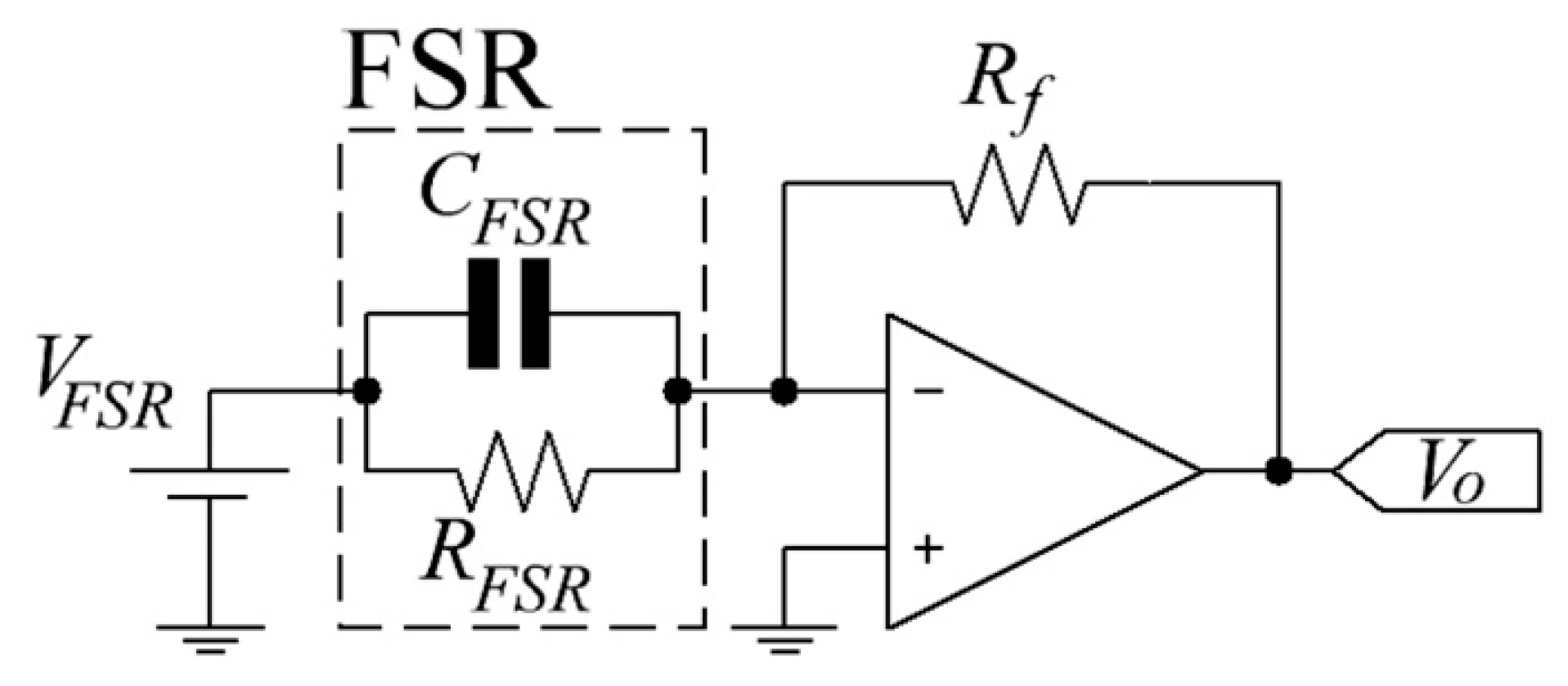
The electrical setup comprised of two circuits: an amplifier in inverting configuration to readout sensor’s resistance, and the authors’ proposed circuit in
Figure 3. The amplifier sketch is shown in
Figure 5, this is the manufacturer’s recommended circuit which is henceforth used as a reference for error comparison [
11]. Given the amplifier in
Figure 5 with sourcing
VFSR, the sensor’s resistance,
RFSR, can be estimated from the following formula:
where
Rf and
Vo are the feedback resistor and the output voltage, respectively. The circuits shown in
Figure 3 and
Figure 5 can drive a single FSR, but multiple FSRs can be simultaneously handled if multiplexers are employed [
22,
37].
Before proceeding with the experimental results, it is necessary to discuss the relationship between the applied stress,
σ, and the parameters
s,
RFSR,
CFSR, and
f. The inter–particle separation,
s, is reduced for larger stresses, and consequently, Equation (2) and Equations (4)–(6) predict a lower
RFSR for incremental stresses. Conversely,
CFSR grows for larger
σ as predicted by Equation (9). The experimental data of
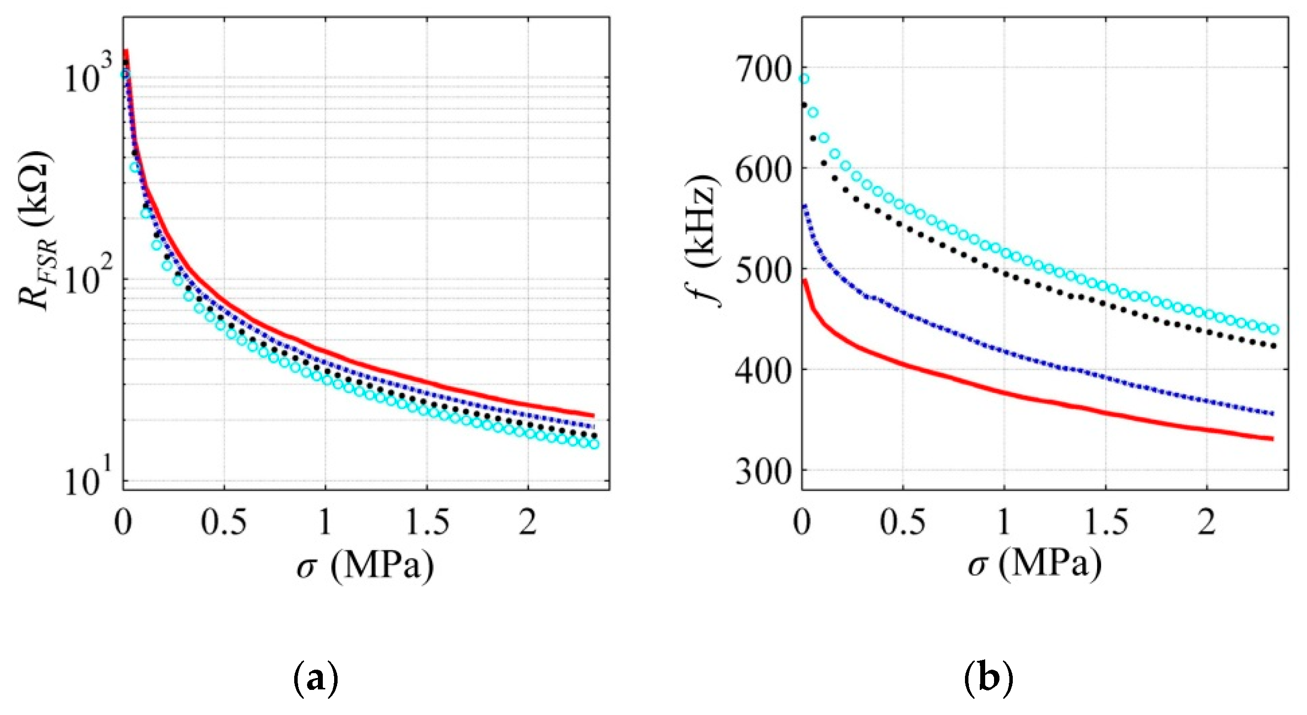
RFSR as a function of
σ is shown in
Figure 6a for the FlexiForce A201-25 sensor at multiple
VFSR. Note that
RFSR is influenced by
VFSR as predicted by the simulation plot in
Figure 2 and Equations (4)–(6).
Figure 6b shows the experimental data for the resulting frequency,
f, as a function of
σ at multiple
Vcc for
R1 =
R2 = 2.2 kΩ. From this plot, several facts can be deducted. First, the larger
Vcc is, the higher
f becomes; this is because
RFSR is lowered with larger
VFSR, thus reducing the time constant. Second, larger stresses yield lower frequencies; this is because the predominant sensing mechanism for a heavily offset sensor is capacitance and not resistance. In other words, considering that
R1 =
R2 = 2.2 kΩ, the parallel connection between
R1 and
RFSR is dominated by
R1, and therefore, the resulting frequency is predominantly modified by
Ce; see Equation (15). Note from
Figure 6a that
RFSR is usually within the range of several tens of kilo-Ohms. And third, the resulting frequency does not linearly change with stress because
CFSR changes with the square root of
σ. This study does not present the experimental data of the sensor’s capacitance, but previous authors’ work does [
30].
4.1. Trimming the Offset Resistances for R1 = R2
The box plots from this Section report on the experimental data from the eight FlexiForce A201-25 sensors under study.
Figure 7 shows box plots for the drift in the resulting frequency at different offset resistances with
R1 =
R2. The data were taken at stresses of 2.3 MPa, 1.15 MPa, and 0.23 MPa that account for 100%, 50%, and 10% of the nominal sensor range, respectively.
Vcc was set to 2.5 V in this test; see the driving circuit in
Figure 3.
The sensors were also tested on the basis of the manufacturer’s recommended circuit (see
Figure 5) at the aforementioned stresses with
VFSR = 1.25 V. However, in this case, the drift errors were calculated from
Vo and not from
RFSR; this was done so because
Vo and
σ are linearly correlated, thus
Vo is the preferred parameter in the literature to determine the stress [
8,
38]. The drift errors in
Figure 7 were estimated at
t = 3600 s using the following formulas:
A sign change was required in Equation (19) due to the inverse proportionality between
f and
σ; see
Figure 6b, i.e., a positive drift in Equations (18) and (19) imply that the measured stress grows over time.
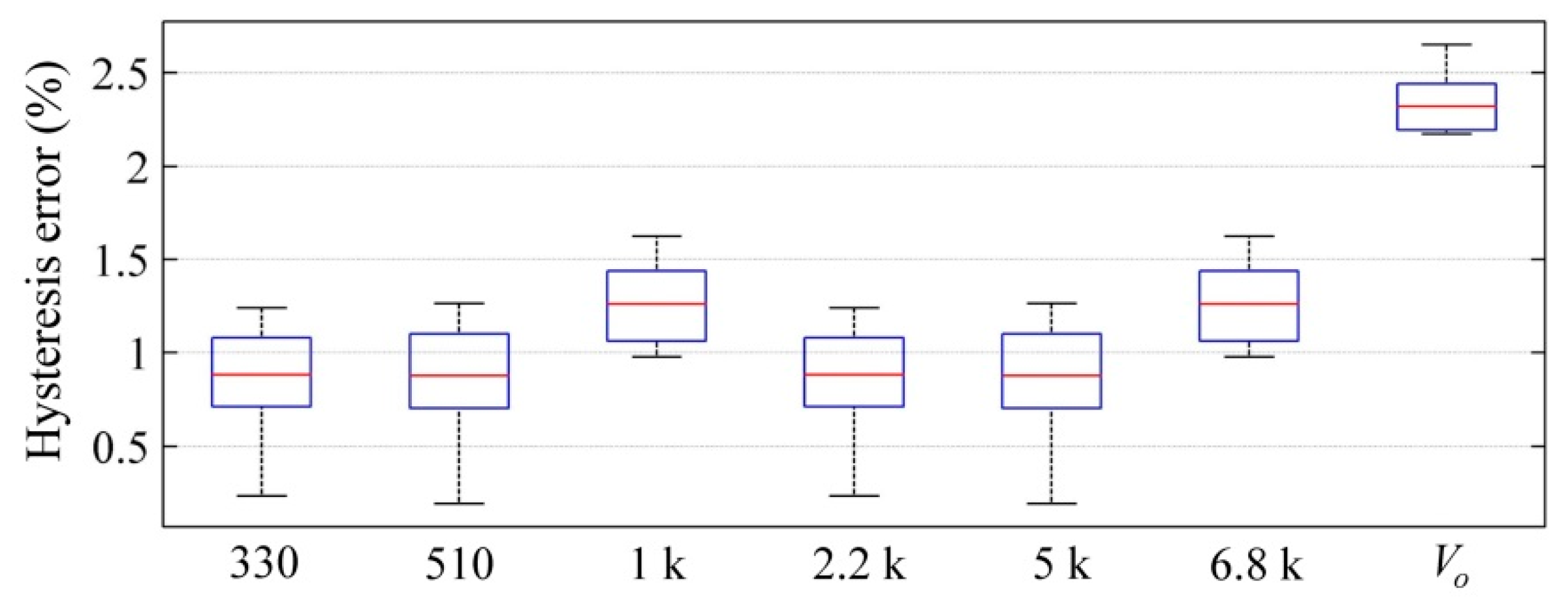
Hysteresis errors were also calculated for
Vo and
f at multiple offset resistances. Box plots for the hysteresis errors are shown in
Figure 8.
According to
Figure 7, a dramatic reduction in the drift error was observed between the authors’ proposed circuit in
Figure 3, and the manufacturer’s recommended method in
Figure 5. Considerable reduction in the hysteresis error is also reported in
Figure 8. Nonetheless, this is not surprising since previous authors’ work has demonstrated that
CFSR measurements yield lower drift and hysteresis errors [
21,
22]. This statement is also supported by the inequality of Equation (10).
Error reduction is greater for the offset resistances within the range 330 Ω–2.2 kΩ, but still, a full compensation of drift or hysteresis was not obtained. Likewise, note that the sign change is never observed in the drift characteristic with the exception in
Figure 7a at
R1 =
R2 = 2.2 kΩ. The drift error is mostly always positive thus indicating that “
εC” dominates in Equation (14), i.e., even for large values of
R1, the drift compensation is never dominated by “−
εR”, but instead, the drift error turns even greater as
R1 is gradually incremented. This may seem as a contradiction at a glance, but it can be explained by recalling that the derivation from
Section 3.1 was obtained on the basis of assuming that
RFSR is many times larger than
R1, see Equation (13). If
R1 is comparable with
RFSR, the approximated formula from Equation (15) cannot be taken as valid, and Equations (11) and (12) and Equation (16) should be used instead.
Unfortunately, if R1 = R2 with R1 comparable to RFSR, the compensation criteria from Equation (14) cannot be fully satisfied because ton in Equation (11) is modified by R1 in a two-folded way, by the parallel connection between R1 and RFSR, and by the argument of the natural logarithm. For incremental values of R1, one term grows and the other decreases, thus limiting the offset effect of R1 in the compensation network. In order to obtain a full compensation of the drift, it is mandatory to independently set R1 and R2.
4.2. Trimming the Offset Resistances for R1 ≠ R2
The offset resistances can be independently trimmed to obtain full drift compensation. The trimming procedure implies setting a fixed R1 and experimentally trimming R2 to satisfy the condition of Equation (14). The opposite procedure (setting R2 and trimming R1) is also possible, but convergence is not ensured given the double dependence on R1 at the ton expression; see Equation (11).
From the box plots in
Figure 7,
R1 under 2.2 kΩ could be chosen to later trim
R2. However, it is desirable to depart from an
R1 that yields low hysteresis and drift errors. It is the user’s decision to choose the most appropriate
R1 based upon the target range of
f. The larger
R1 is, the lower the resulting frequency becomes, see Equations (11)–(16). There are multiple combinations of
R1 and
R2 that satisfy Equation (14). The authors have chosen
R1 = 510 Ω as the value to later trim
R2.
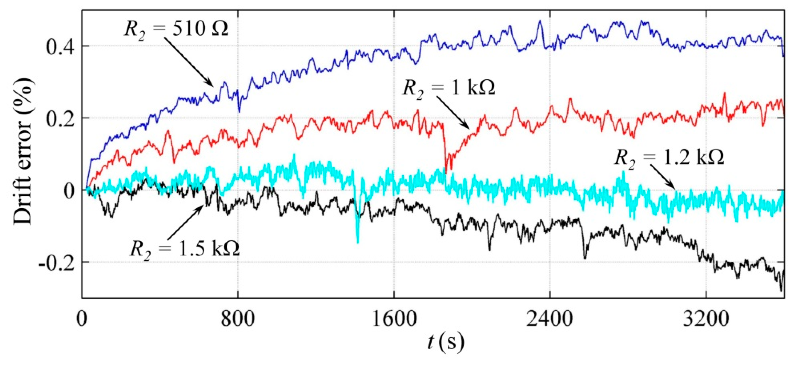
Figure 9 shows the time plots of the drift in
f at different
R2 with errors estimated from Equation (19). The applied stress during this test was 1.15 MPa. Note that as
R2 grows, the drift characteristic is gradually dominated by “−
εR”, whereas the “
εC” component is progressively diminished. In the limit case when
R2 = 1.5 kΩ, the resulting drift is negative thus indicating that “−
εR” dominates.
Full compensation of the error was obtained for this specimen when
R2 equals 1.2 kΩ. However, the frequency signal is somewhat noisy at 0%. The authors can only hypothesize about the possible source of the noise. The experimental observations from the previous authors’ work demonstrated that the effective area for tunneling conduction,
A, is modified by the applied stress [
19]; see Equation (7). If
σ is held constant for an extended period of time, the authors believe that
A fluctuates in a random fashion, thus, causing the noise in
Figure 9. It must be highlighted that
A modifies both
RFSR and
CFSR, as predicted by Equations (4)–(6) and Equation (9). An experimental fact supports the hypothesis of a randomly fluctuating
A as the source of the noise. If the drift experiment is repeated at the same electromechanical conditions, a somewhat different noise pattern is observed. To the authors’ criteria, this occurs because the tunneling paths can be created or destroyed over time amidst a constant
σ. Each specimen of FlexiForce A201-25 sensor exhibited a different
R2 for obtaining full drift compensation.
It is logical to suppose that the noise in
Figure 9 is produced by the random behavior of the inter-particle separation. Nonetheless, to the authors’ criteria, this is quite unlikely to happen, because
σ and
s are correlated by rheological models which are non-negative functions [
31], and therefore, the negative phase of
drift_f cannot originate from an increment of
s amidst constantly applied stress.
The authors do pay a lot of attention to the electrical noise in
Figure 9 because it may indicate that the theoretical limit of accuracy has been reached for the FlexiForce A201-25 sensor, i.e.,
Figure 9 indicates that no matter what the compensation network is, the measuring uncertainty is held around 0.1% of the applied stress. Reducing the noise in FSRs is also an active research trend. For instance, Wang and Li have demonstrated that the vulcanization of the sensor’s electrodes is an effective method for reducing noise in such devices [
39]. Nonetheless, it must be remarked that a measuring uncertainty of 0.1% is a very good result considering that a repeatability error of 2.5% has been stated in the sensor’s datasheet [
11].
A comprehensive model has been developed by Sheng [
40] for the electrical noise in tunneling conduction. Given the small number of free electrons in the conductive nanoparticles, they result in being very sensitive to the transient deficits or excesses of charges. When this occurs, voltage fluctuations appear across the multiple tunneling paths, causing electrical noise.
4.3. Testing the Authors’ Proposed Circuit
In order to comparatively test the authors’ proposed circuit with the manufacturer’s recommended method, the following test signal was applied to the sensors for a time span of five hours:
The dynamic signal from Equation (20) aims to test the sensors in a comprehensive way. The occurrence of sensitivity degradation is assessed through the sine component. Likewise, drift is also evaluated since the smallest value of stress is 0.21 MPa in Equation (20), which corresponds to a minimum force of 9.8 N.
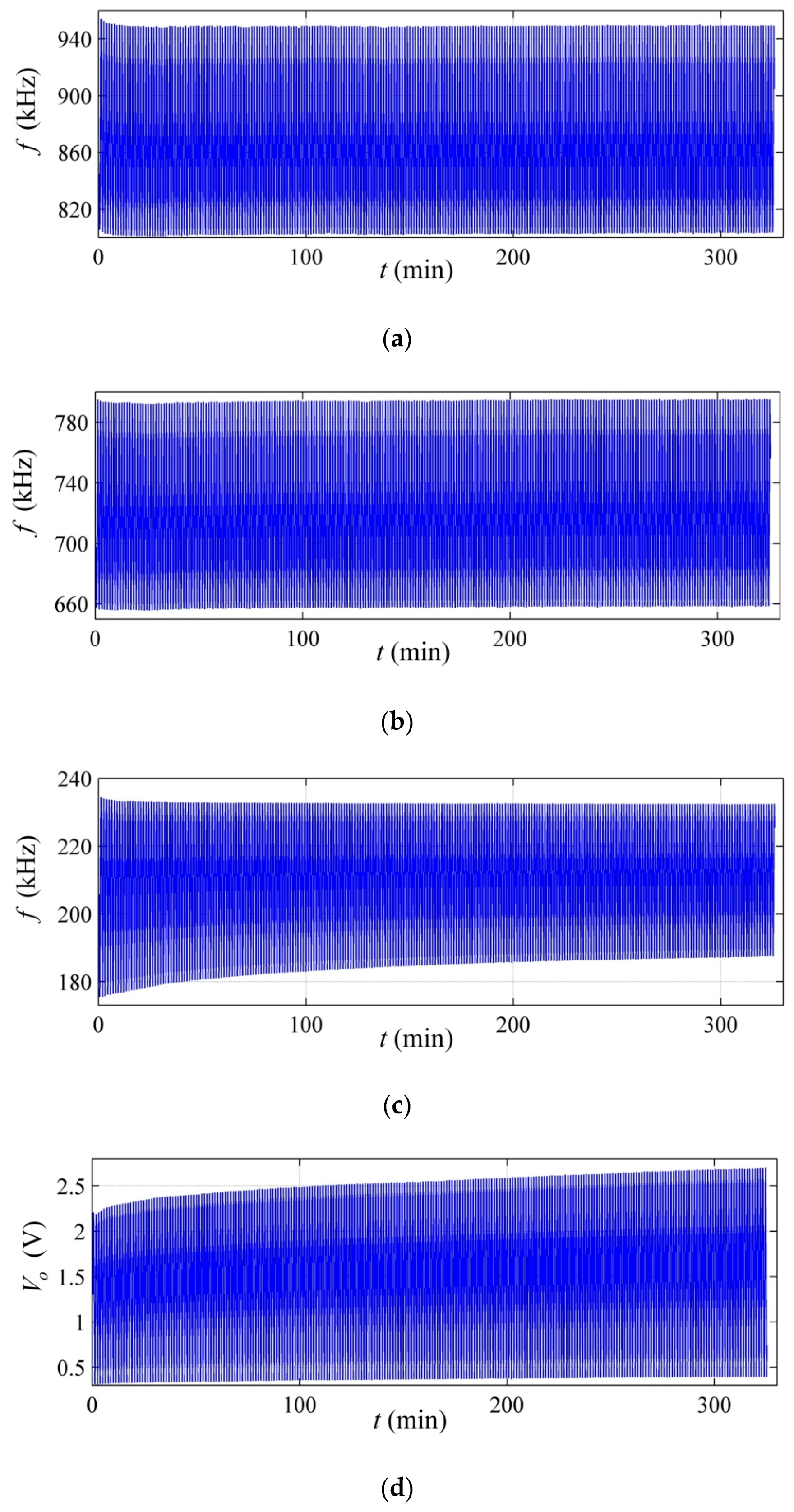
Figure 10a–c show the time plots of the resulting frequency for different values of
R1,
R2, and
Vcc. The manufacturer’s recommended method was also tested with the stress signal of Equation (20) at
VFSR = 1.25 V; see
Figure 10d. The plots in
Figure 10 show the experimental data for a single specimen of the FlexiForce A201-25 sensor, but the statistical data from the eight specimens are presented in
Table 1 using the Root Mean Squared Error (RMSE) as the metric to assess the performance of each method. In order to obtain the RMSE, the
f–
σ curve of each sensor was fitted to a third-order polynomial function and then, the applied stress was estimated from the frequency measurements. On the other hand, the stress estimation in
Figure 10d was possible from a first-order polynomial fit on the basis of
Vo measurements.
Given the
f and
Vo measurements, and the polynomial models, the measured stress (
σmeas) could be computed for each method. The RMSE was later calculated by taking the load cell data from
Figure 4 as the reference for the error calculation.
The smallest RMSE was obtained for the experimental set up with
R1 = 510 Ω,
R2 = 1.2 kΩ, and
Vcc = 2.5 V (
Figure 10b); this is not surprising given the fine-tuning presented in
Figure 9. The experimental setup with
R1 =
R2 = 510 Ω (
Figure 10a) exhibited a somewhat larger RMSE, but still, the resulting RMSE is almost four times lower than the error resulting from the manufacturer’s recommended method in
Figure 10d. It must be recalled that the resistance drift is always larger than the capacitance drift—see Equation (10)—and consequently, the circuit in
Figure 3 always yields a lower RMSE because frequency variations are predominantly modified by capacitance changes.
The plot in
Figure 10c exhibited sensitivity degradation, and therefore, the largest RMSE was obtained with this experimental setup. Sensitivity degradation was not observed in
Figure 10d because
VFSR was held low at 1.25 V. Readers may refer to References [
32,
35,
36] for experimental results showing the sensitivity degradation for the setup in
Figure 5.
The experimental results in
Figure 10 and
Table 1 demonstrate that the authors’ proposed circuit is an effective method for reducing the measurement errors in FSRs.
4.4. Comparing the Performance of the Authors’ Proposed Circuit with Manufacturer Data (datasheet)
Providing a comparison with manufacturer data may result confusing because the manufacturer does not specify the full test conditions in the sensor’s datasheet [
11]. In previous studies, the authors have demonstrated the influence of the sourcing voltage on the sensor’s performance [
19,
20]. Unfortunately, the sensor’s datasheet only specifies the mechanical conditions when the sensor’s performance was evaluated [
11].
Table 2 provides a comparison among three different sources: the authors’ proposed circuit in
Figure 3, the sensor’s datasheet [
11], and previous experimental data from the circuit in
Figure 5 at multiple voltages [
20]; it must be remarked that the circuit in
Figure 5 is the same employed in the sensor’s datasheet.
5. Conclusions
Force Sensing Resistors (FSRs) exhibit an opposite sign in the drift characteristic of sensors’ resistance and capacitance. This behavior can be used to design a self-compensated driving circuit. The proposed compensation method is based on a modified-astable 555 circuit in which the FSR was configured to charge and discharge in an oscillating basis. Given the larger drift in the sensor’s resistance, it has been conveniently offset to match the lower drift in the sensor’s capacitance; this was done from a fixed resistance connected through the charge and discharge paths.
Experimental results of the modified-astable 555 circuit yielded a dramatic reduction of the drift and hysteresis errors (by a factor of 9 in the drift error and a factor of 3 in the hysteresis error) when compared with the manufacturer’s recommended method, which is based on an amplifier in the inverting configuration.
The output frequency (f) of the modified-astable 555 circuit was successfully correlated with the applied stress (σ). This allowed for the estimation of unknown stresses on the basis of f measurements. The f-σ relationship was not linear, and therefore, a third-order polynomial fit was required for this purpose.

 ,
, 


