Performance Analysis of a 3D Wireless Massively Parallel Computer

Department of Computer Science, University of York, York YO10 5DD, UK
*
Author to whom correspondence should be addressed.
J. Sens. Actuator Netw. 2018, 7(2), 18; https://doi.org/10.3390/jsan7020018
Submission received: 28 February 2018
/
Revised: 5 April 2018
/
Accepted: 10 April 2018
/
Published: 19 April 2018
(This article belongs to the Special Issue Energy Efficient Networking)
Abstract
:In previous work, the authors presented a 3D hexagonal wireless direct-interconnect network for a massively parallel computer, with a focus on analysing processor utilisation. In this study, we consider the characteristics of such an architecture in terms of link utilisation and power consumption. We have applied a store-and-forward packet-switching algorithm to both our proposed architecture and a traditional wired 5D direct network (the same as IBM’s Blue Gene). Simulations show that for small and medium-size networks the link utility of the proposed architecture is comparable with (and in some cases even better than) traditional 5D networks. This work demonstrates that there is a potential for wireless processing array concepts to address High-Performance Computing (HPC) challenges whilst alleviating some significant physical construction drawbacks of traditional systems.
1. Introduction
In an HPC system there is a constant need for increasing the density of processors within a given volume. However, there are limitations that occur when wired interconnects and traditional 2D Printed Circuit-Board (PCB) modules are stacked. Also, the thermal issues become more serious in a system that achieves higher density and ever faster CPU cores, leading to the need for liquid cooling. Both issues indicate that a high-density system should attempt to eliminate traditional 2D PCB planes and avoid hard-wired interconnects if realistic alternatives can be employed. The purpose of our evaluations, in this paper, is to determine if the performance constraints for such a system are within the range that makes them competitive with existing systems, and ultimately more capable, as scaling reduces the size of nodes and increases the number of nodes in an array.
Wireless technologies have not been regarded as serious options for an interconnect network in high-performance computing thus far. This is mainly because of their size, energy demands and transfer rates. Considering new developments in on-chip high-speed wireless devices, we are now close to a viable wireless interconnect network for a massively parallel computer. These technologies have narrowed the gap between wireline and wireless devices. One reason why wireline data rates do not increase as fast as wireless devices is that wireline transceivers are close to reaching their performance limits [1].
There is a separate (yet closely related) field of research in which independent agents collaborate with each other to perform a computationally heavy task. Generally referred to as Swarm Computation, it can be regarded as a variation on swarm robotics. The key issue in swarm computing (and swarm robotics in general) is to take advantage of the flexibility of the agents in configuring and re-configuring and re-configuring themselves to tackle different tasks depending on changes in circumstances (e.g., [2]). Among applications for such a concept is computation in hazardous or remote environments like spacecrafts [3].
Another characteristic of such platforms is the higher level of intelligence or computation power emergent from collaboration of agents with lower intelligence. Swarm computing does have some overlap with the work presented here and offers significant potential for future avenues of work; however, the differences between these two fields should be noted. This paper presents a novel interconnect network for a massively parallel computer. Although the interconnect network we proposed can be regarded as reconfigurable in the sense that new nodes can be added to it, the topology of the network is fixed during normal operation. Moreover, the dynamic reorganization of nodes has not been considered in our work to date.
In our previous papers [4,5] a 3D wireless grid was introduced for a novel parallel platform called A Ball Computer (ABC). It can scale easily since there is no wiring limitation. Other advantages of such a platform are significant reduction in network cost and complexity. However, there are some critical issues, such as wireless power delivery and heat dissipation. Hind [6] and Kamali [7] have investigated several options for those issues. Hind [6] has shown that there are some promising options for wireless power delivery; however, they still need to be more mature for a viable solution. This paper focuses on connectivity in the ABC and its impact on the nodes’ and links’ performances.
This research considers the impact of a novel combination of two concepts: wireless interconnect technology and a 3D structure with hexagonal lattice topology. However, to the best of our knowledge those concepts have been combined for such an application for the first time in our evaluations.
The ABC envisages a computer system made of balls (1–2 cm in diameter) each containing computing and communicating elements that can be rapidly and cheaply assembled. It supports a wireless 3D hexagonal lattice of a substantial number of processors, which can operate as a massively parallel platform.
In previous work [3], our evaluations suggested that for a set of tasks and network attributes the ABC’s processor utilities are comparable to modern HPC platforms. Our new work incorporates additional critical issues, specifically link utilisations, and we employ a store-and-forward packet-switching algorithm. Performance comparisons are then made between the ABC and a 5D topology (which is used in supercomputers like IBM’s Blue Gene series). We will demonstrate that, when these new factors are included, for a specific set of tasks the ABC’s performance is comparable to 5D topology. However, we also observe that a store-and-forward switching method has a negative impact, particularly on the link utility.
The rest of this section is dedicated to a brief review over current short-range high-speed wireless technologies and packet-switching methods. The paper continues with a brief introduction to the ABC architecture in Section 2. Results from simulation experiments are presented in Section 3. The ABC’s 3D topology and a 5D topology are compared based on both link and processor performances. The paper finishes with conclusions and considers ideas for future work in Section 4.
1.1. Wireless Technologies
A wireless communication technology for the ABC’s should meet some criteria over size, energy consumption and transfer rate, among others. A review of three wire-free data transfer methods is given in previous papers [4,5,7].
In capacitive coupling, data is transferred using the electrical charges on a capacitor’s plates. The power consumption is less than 1 pJ/b (see Figure 1a). It occupies small area per channel. Data rates are usually very high (Myat et al.’s [8]). It is possible to use grids of channels in parallel: 260 Gb/s using 144 channels [9] and 32 Gb/s using 128 channels [10]. Capacitive coupling rarely supports distances over 10 µm. It is highly sensitive to misalignment of facing pads of capacitors.
In inductive coupling, data are stored inside a coil to be transferred to a coupled coil. Data rates are in a range of gigabits per second (e.g., 1.1 Gb/s by Matsubara et al. [11] and 8 Gb/s by Miura et al. [12]). It is possible to use grids of channels in parallel (1024 parallel links with 8 Tb/s by Miura et al. [12]). It is very space-efficient with very low power consumption (see Figure 1b). The links are up to a few hundred micrometres. Lower link distances, less than 10 cm, links with lower data rates (e.g., Lee et al. [13]) are proposed for a wearable body area network.
On-chip mm wave RFs have historically suffered from their size, the power they consume, the high volume of noise added to the signal, packet collision and signal interference intensified by their long range; however, energy consumption has fallen recently (see Figure 1c). The most popular frequency bands are 60 GHz and 120 GHz [14,15]. A THz band is feasible [16,17]. The occupied area per radio module differs (e.g., from 0.05 mm2 in Foulon et al. [18] to 56 mm2 in Miyashita et al. [19]). Mm-wave RF is a well understood and robustly researched technology.
Figure 1 collates data from a number of studies in the three aforementioned technologies. Figure 1a plots capacitive coupling technologies [8,10,20,21,22,23], Figure 1b summaries inductive coupling [13,24,25,26,27,28] and Figure 1c belongs to mm-wave on-chip radios [29,30,31,32,33,34,35,36,37]. Figure 1 shows that the energy consumption in all three categories have dropped over the last 15 years. It should be noted that values in this figure are normalised and therefore cannot be 100% accurate, but the general trend of reduction in energy can be seen. Sources of this inaccuracy include differences in design, link length and bit error rate in different works.
Three categories of wireless technologies are compared against three main criteria: data rate, energy consumption and communication distance. Figure 2 shows that only a few on-chip radio devices can satisfy all the criteria. 1 Gb/s is selected for the lower limit for data rate criterion. It is hard to identify a lower limit for energy consumption. An approximated 10 pJ/b energy consumption is used as a lower limit (see [7]). The on-chip radio devices that satisfy these criteria are listed in Table 1.
It should be noted that the results in Figure 1c do not match the distance, and data rate criteria; therefore, Figure 1c and Table 1 do not share the same results. Table 1 shows that the best energy consumption per bit per mm has been around 0.0005 pJ/bit/mm in recent years, which is approximately 0.05 pJ/bit for a 1cm distance (based on the rule of inverse square). This means the overall power consumption is in the range of 1 mW for a 20 Gb/s transceiver.
In the remainder of this paper, on-chip mm wave RF approach is utilised in our simulations, mainly because they support cm-long transfer ranges. For a review on reactive and radiative communications the reader should refer to Moore et al. [1] and Rabaey et al. [48]. In our chosen model, we assume a range of data transfer between 100 Kb/s and 1 Tb/s and a power cost below 1 pJ/bit. In current technologies, such a power consumption is realistic.
1.2. Packet-Switching
Three packet-switching methods are reviewed in this paper.
1.2.1. Store-and-Forward
Store-and-forward algorithms are based on the idea of relaying a message only after receiving all of it in an intermediate node. Such algorithms are easy to implement but on the negative side, the intermediate nodes leave the output channel unused until the whole package is received, which loses considerable time. In this method, the overall multi-hop transfer time relates to the number of hops, which in turn is relevant to the software and hardware latencies. This is a significant issue in direct networks.
1.2.2. Cut-Through
The main objective of this method is to start relaying a packet in an intermediate node before receiving the entire packet. This makes some overlap between using the input and output channels; and consequently, the link utilisation is improved, and overall parallel execution time is decreased. In practice, the output streaming starts after receiving the first 14 (or 64) bytes of incoming packet [49].
Guaranteed continuation of data streams, in transmitter and receiver links, are needed; otherwise it may not yield satisfactory results. Handling of corrupt packets is another issue in cut-through method as the CRC (Cyclic Redundancy Check) sequence is normally the last part of a packet. This may lead to a decrease in effective link utilisation. This can be a bigger issue when dealing with wireless links in which the corruption may be detected only on the final receiver side. It may end up in a situation in which a packet is relayed in a whole chain of hops only to detect its corruption in the last hop. Another issue is the necessity of having the same transmission speed on both input and output channels; otherwise there would be no simultaneous streaming of data in and out of a node.
1.2.3. Wormhole
This method extends the idea of cut-through routing by introducing the concept of virtual channels (VC). It is based on the idea of splitting a packet into smaller pieces called flits (flow control digits). The first flit of a packet (the header flit) contains the data needed for routing with or without a part of real data. It can be followed by 0, 1 or more than 1 data flits. Several VCs can be associated with 1 physical channel. Each of these VCs is dedicated to the transmission of a unique packet.
The difference between flits and packets is that two packets with the same source and destination may go through different paths and may not be received in the same order as they have been sent. However, two flits of a packet always pass through the same path and in the exact order as they have been sent. Also, a packet, unlike a non-header flit, has everything needed for routing. It is the VC mechanism that handles the routing for header-less flits. On reception of a header flit in an intermediate node, proper network resources are allocated before relaying. The same resources are used for the rest of the flits of that packet.
This is the algorithm of choice for many modern HPC systems like Cray’s 3D torus Gemini, Dragonfly-based Aries, and Flattened Butterfly technologies. It reduces the overall software latency and increasing the throughput. Cut-through and wormhole methods try to decouple the relation between the overall transmission latency and the number of hops.
2. Ball Computer Architecture
In this section, two topologies are presented to implement the idea of A Ball Computer. One of these models is simulated in a simulation toolkit. The performance measurements and analyses in Section 3 are based on those simulation experiments.
2.1. 3D Hexagonal Topology
A 3D hexagonal topology is chosen to implement the ABC concept. In a 3D hexagonal topology (Figure 3b) each node (other than edges and corners) has 12 neighbours. A face-centred cubic (FCC) formation has geometrical symmetry and reduces the space occupied by the network. It is shown that it is the most compact formation of spheres in a hexagonal topology. Gauss [50] has proven that the packing density of the spheres in FCC is . There is still more than 25% of the volume available for cooling with a single contiguous coolant space.
Table 1 shows that on-chip radio devices are the best technologies for the ABC. Apart from energy consumption, the main problem with radio devices is packet collision caused by the hidden-node problem. A multi-channel scheme is used to stop packets corrupting each other. Each node has eight radios tuned to different channels. A network partitioning and channel assignment algorithm guarantees no collision between packets.
Those algorithms are designed to eliminate packet collision and at the same time minimise the overall number of channels. The first algorithm partitions the network into zones. Inside a zone there would be no hidden nodes. Zones in 2D and 3D grids look like a triangle and a pyramid, respectively (Figure 4 and Figure 5).
The second algorithm assigns channels to zones so that there is no signal interference between any two zones and at the same time the number of channels is minimal. These two algorithms guarantee that there would be no packet collision either inside a zone or between zones.
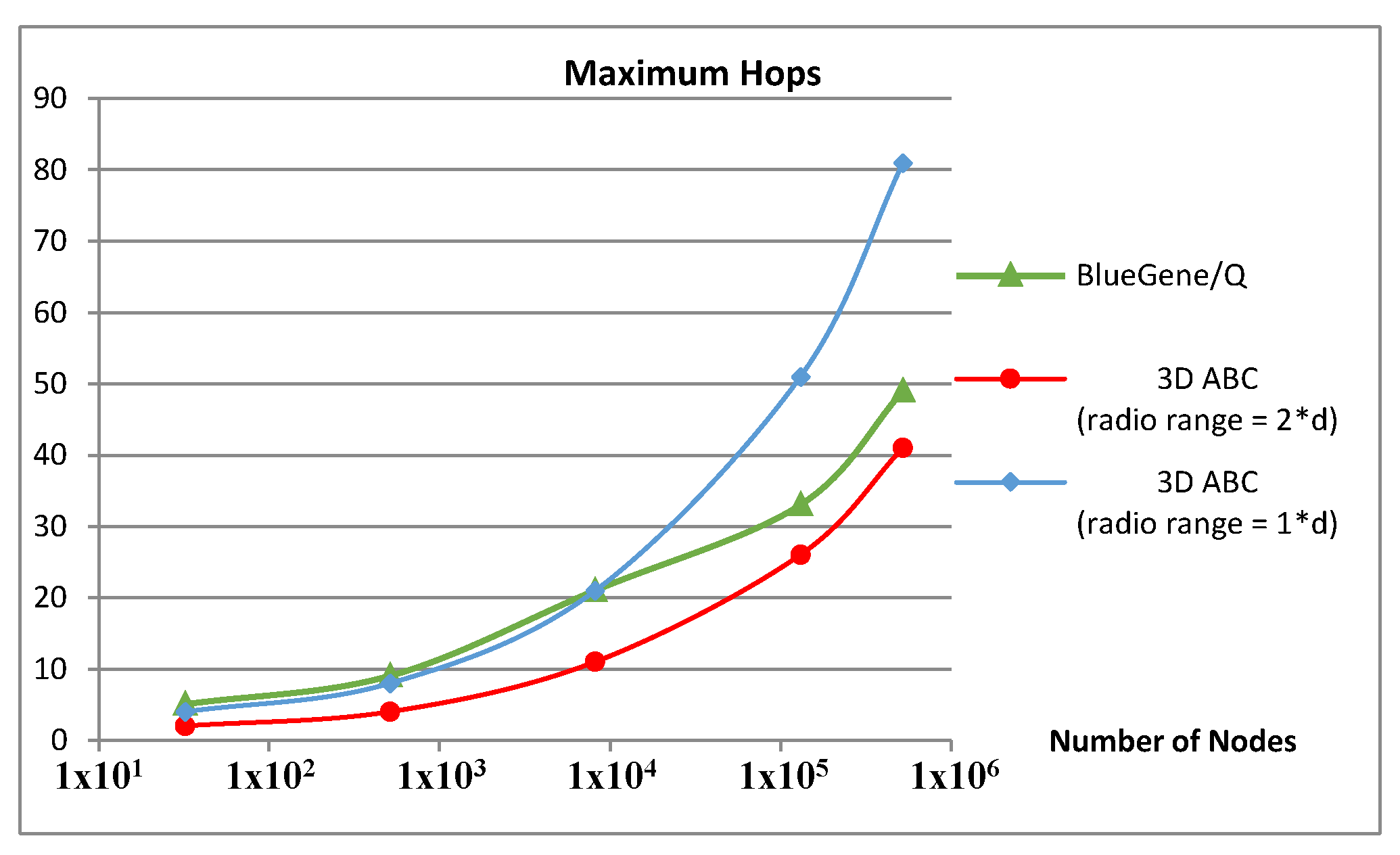
Depending on the range of radio communication the number of the zones may vary. Figure 6 compares the number of hops in a 5D direct network (like IBM’s Blue Gene) with a 3D ABC platform with two different radio ranges. The performance of ABC is highly dependent on the number of neighbours each node can contact directly. Two cases are compared in Figure 6. The blue graph represents the case in which each node only communicates with its direct neighbours. The radio range is bigger in the red graph so that it can directly contact its immediate neighbours as well as their respective neighbours. For small and medium-size networks (fewer than 8000 nodes), the number of hops in a 3D ABC is lower than in a 5D network.
2.2. 4D ABC Topology
A ball in a 4D topology for the ABC consists of eight independent modules (Figure 7). Each module has two processors and six transceivers. Eight modules are connected to form a cube (with chopped edges).
The transceivers provide both intra-ball connectivity (between modules inside a ball) and inter-ball connections. This topology has an advantage over a formation of processors in a flat surface or in a matrix fashion in the sense that it leaves enough empty space inside a ball and holes in each side of it to let the cooling liquid flow through.
A ball (as shown in Figure 7) has 16 processors. They are connected as a {2 × 2 × 2 × 2} 4D hypercube (Figure 8). The network can only grow along the first three axes (x, y and z). Such a topology decreases the number of hops compared to the 3D topology (discussed in Section 2.1) for large networks. For the rest of this paper we only focus on the 3D ABC architecture. In the future, more research is needed to measure the performance of the 4D ABC topology.
3. Simulation Results
A simulation/visualisation toolkit is implemented to measure the performance of the 3D topology (Section 2.1) of the ABC. A store-and-forward packet-switching method is used mainly for the sake of simplicity of implementation. This is an ideal-world model with zero inter-channel interference. Various sources of noise will be modelled for future work.
A network protocol is deliberately implemented in a minimal form, so that it only covers the concepts that have the highest impact on the network performance. To follow the tradition of high performance computing platforms, ABC is envisaged to operate in a restricted environment. This means that the network will have a fixed topology (with the possibility of manually adding or removing nodes). Moreover, the communication protocol is not subject to change over the course of ABC operation.
In this study, we are primarily concerned with feasibility and practical limitations based upon existing technologies; therefore, a more comprehensive bespoke electronic design process is anticipated to be a focus of future work and follow-on studies. There are important electronic design issues that deserve an extensive selection process, including what mm-wave technology to use and what type of antenna to choose so that the balls can be made with envisaged size and functionalities. These are main topics for the next phase of this research in which a real-world prototype of ABC will be built.
The results are based on experiments with a Java network simulator developed by our team. The simulator runs on an HPC platform owned by the ACAG, University of York. The transfer rates are chosen to represent the present technologies as well as potential technologies in the future; therefore, some of the transfer rates are not available now. Regarding the level of abstraction this simulator runs on, there is no need to implement the electronic details of the communication devices. What we are interested in are the transfer rate, the distance and the power consumption of the links. It should be noted that, should a different level of simulator abstraction be chosen, other features of the communication protocol would be modelled as well; however, regarding the current abstraction model, there is no need to include any other features. Also, it is the same for hardware implementation of the transceivers (e.g., antenna technology), which are outside the scope of the simulator.
Instead of real-world tasks, a high-level abstraction (referred to as a task model in this paper) is used for the simulations to keep distance from the trivial details of tasks. A task model is an artificial packet generator that mimics the communication behaviour of a class of tasks in real-world. In this paper a divide-and-conquer task model is used that is inspired by Fast Fourier Transform (FFT) operation. The FFT Task model (FFTTM) splits a bulk of data into pieces and shares it with other nodes for parallel operation. The task model uses a load balancing mechanism to tune the size of data for each node based on the overall number of hops needed. More details on the simulation tool including the communication protocol used and the architecture of each node can be found in [4,5,7].
The main target of the experiments is to verify the efficiency of the routing algorithm and the FFTTM in a 5D network and a 3D ABC. The behaviour of the ABC network is measured under different network sizes, link transfer rates, processor data sizes and computational ability. At the end we can compare the performance in those topologies. In each test, eight workloads are running with overlaps over their execution time.
The performance is measured based on two categories: processor and link utilisations. The processor utilisation (PU) shows what percentage of the processors are engaged in a parallel operation on average. The link utilisation includes link busy time, link access wait time and the link effective busy time, which is the time needed to send real data (excluding packet retries, network inventory packets or a packet’s header and footer).
The applied simulation methodology assumes a system containing 1000 and 2000 nodes, and therefore simulation times and resources can be demanding with certain parameters. As a result, we made use of overlapping ranges of parameters to gain a wide range of performance trends. The disadvantage is that some extreme data points are omitted from our performance curves, as can be seen in certain figures introduced later (Figure 11f and Figure 14f for example). Nonetheless, in general, the presented performance curves cover the points of interest to our analysis.
Two topologies: a 5D direct network inspired by Blue Gene topology, and a 3D ABC, are used in the experiments. Each topology is applied to both 1000 and 2000 nodes. The chosen task model is FFTTM in all experiments. Three data sizes are used (100 KB, 1 MB, and 10 MB). The transfer rates are 100 Mb/s, 1 Gb/s, 10 Gb/s, 100 Gb/s, and 1 Tb/s, respectively. The nodes’ computation power is 10 MIPS, 100 MIPS, 1 GIPS, 10 GIPS, and 100 GIPS, respectively. Not all these values necessarily reflect the reality of computation or transfer capability of real-world devices. They are used only to give a picture of the performance of these two topologies over a wide range of attributes. The key variable is the ratio of the communication speed divided by the computation capability (comm/comp ratio). Our tests have shown that with small values of comm/comp ratio (0.001, 0.01 and 0.1) the performances are very poor and at the simulation time is very long. For these reasons the tests with comm/comp ratio equal to 0.001 and 0.01 (and 0.1 in some cases) are excluded from our experiments.
3.1. Processor Utilisation Analysis
A processor’s computation time is estimated by the total number of simulation iterations in which the processor is busy with computation. The overall computation time is the sum of the computation times of all processors. The PU is the overall computation time divided by the number of nodes then divided by the simulation time (in iterations) expressed as a percentage.
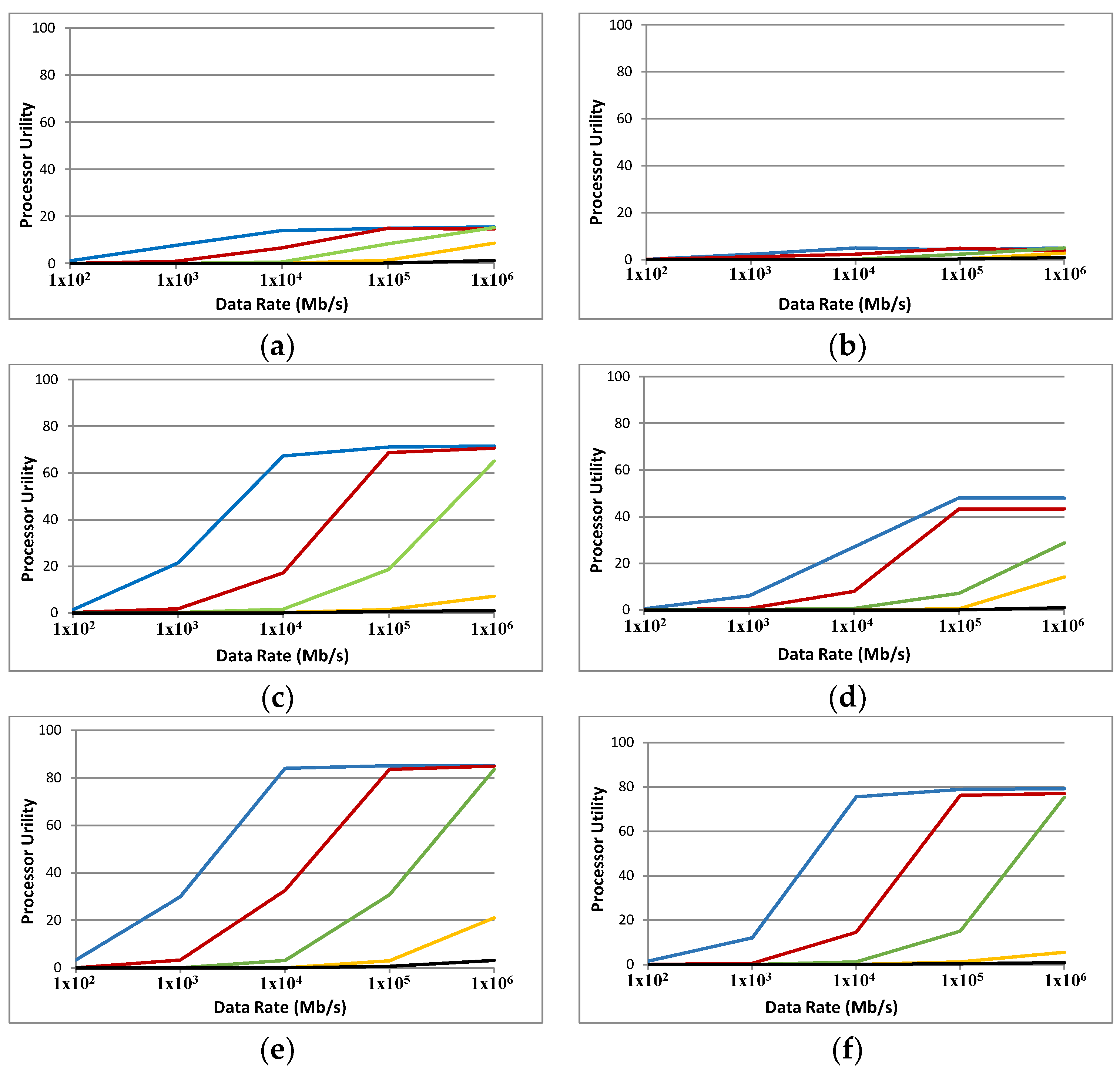
The experiments with ABC (Figure 9) show that in many cases PU increases with an increase in comm/comp ratio. It is only at a very high data rate of 1 Tb/s that PU levels (or drops a little bit) compared to 100 Gb/s. The simulated grid yields better PU with larger sizes of data. The best results (up to 84%) are achieved with 10 MB of data and the comm/comp ratio above 10,000. Regarding the available technologies (data rates between 10 to 100 Gb/s), PUs of around 60% to 80% are predicted (see blue plots in Figure 9c,e,f). Note that a multi-channel communication scheme is envisaged for the ABC. The available bandwidth will be divided between channels which lowers the available bandwidth for each channel, and the PU will be lower as a result.
The results with a 2000-node ABC (in Figure 9b,d,f) are the same as with 1000 nodes. However, there is a decrease in PU with 2000 nodes compared to 1000 nodes. The nature of the task model and the packet-switching method can be responsible for this. Expansion of a network brings potential for an increase in PU and consequently faster task completion; however, the task model used in these simulations seems unable to take advantage of that opportunity.
The same experiments are made with a 5D grid (Figure 10). The PUs in ABC and 5D grids are comparable. In some cases, the ABC performs slightly better than the corresponding experiment with 5D. Like the ABC grid, with a 5D grid the same trend of increase in PU with an increase in comm/comp ratio and data size is observed. Again (like with ABC), there is a performance plateau with some data points with a data rate = 1 Tb/s.
3.2. Link Utilisation Analysis
OLBT (Overall Link Busy-Time) and OLWT (Overall Link Wait-Time) are two performance measures used in this paper. A link’s busy time is estimated by the total simulation iterations in which a node was using that link. This estimated link busy time is calculated for each node and their summation estimates the overall link busy-time (OLBT). Overall link wait-time (OLWT) is calculated in the same way by summation of the iterations in which a node was waiting to access a link. Both measures are in milliseconds (a fixed time unit) instead of simulation iterations, which is a varying time unit. Moreover, OLBT is compared to a hypothetical non-overhead data transfer mechanism. This is an indicator of the efficiency of the communication protocol, as it shows how much communication was dedicated to real data instead of overhead, re-transmissions, ACK packets, etc. To make it possible to compare the results, the experiments are grouped in terms of data size and comm/comp ratio. It should be noted that in all experiments FFTTM is used; therefore, the results reflect the combination of task model-specific behaviours, communication protocol and network topology. Other task models are likely to produce a completely different set of results.
3.2.1. Overall Link Busy Time
OLBT is measured in ABC (1000 and 2000 nodes) with FFTTM (see Figure 11). The general trend of a decrease in OLBT with an increase in data rate is observed for most data points; however, the slope of this decrease varies from point to point. In some data points corresponding with low processor capabilities, OLBT does not change much as data rate increases (e.g., parts of blue plots in Figure 11a–c and red plots in Figure 11a,b,f). A reduction in OLBT can be caused by several factors. A majority of potential factors that may contribute to the behaviour of OLBT is fixed in ABC. Hardware design (e.g., antenna design and amplifying system) and the link distance do not change and cannot influence on OLBT. This means that the communication protocol (the store-and-forward algorithm in particular) used in the simulation cannot take advantage of very high comm/comp ratios. It is anticipated that a cut-through or wormhole mechanism will perform better.
OLBT is also measured for a 5D network (Figure 12). The same inverse relationship between the data rate and OLBT is observed in most cases. Compared with a 5D topology, the ABC has a slightly sharper decrease in OLBT when the data rate increases. More analysis is needed to identify why in some odd cases the OLBT remains unchanged (or has a slight increase) as the data rate increases (e.g., blue plots in Figure 12a–d, but, so far, this effect can be related to the very high data rates. This means that the links are close to their hard limits of performance and an even faster transfer rate has little chance to make a real difference. OLBT has a direct relationship with the overall power consumption of a network like ABC as data transfer over radio links is an energy-demanding process. The role of OLBT in the overall execution time will be discussed later in this section by comparing the simulation results to a hypothetical non-overhead communication mechanism.
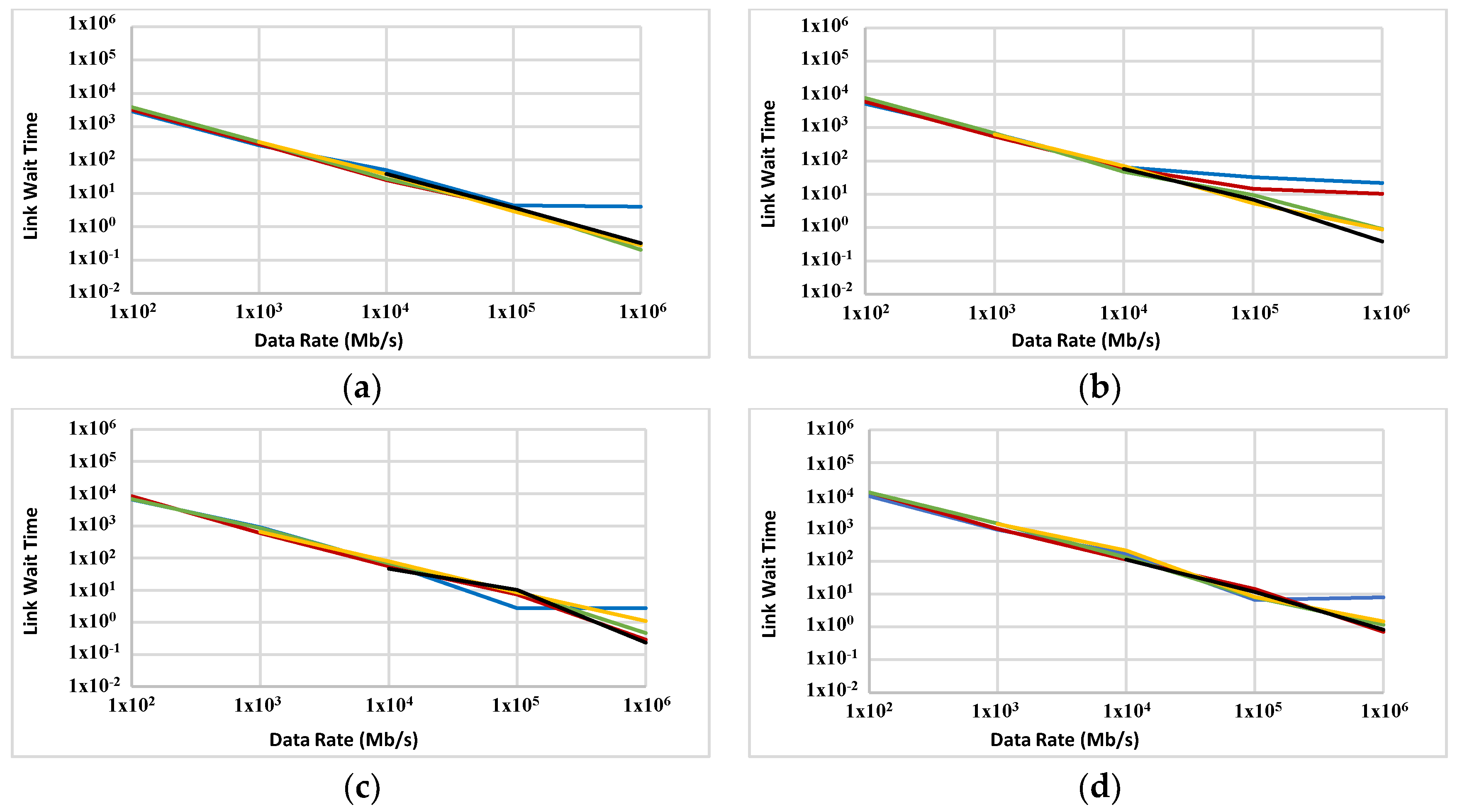
3.2.2. Overall Link Wait Time
OLWT is measured on the ABC and a 5D network (Figure 13 and Figure 14, respectively). Like OLBT, the decrease in OLWT because of the increase in data rate is observed for most data points in both figures. The slope of decrease in OLWT is slightly steeper for the ABC compared with a 5D network.
OLWT is an estimate of how long nodes have been waiting to access the links. Since the simulated nodes are multi-tasking, they can yield control to another task when they are waiting for link access. This makes OLWT a less crucial factor for measuring the performance of the proposed network. However, it still has importance, especially at the final stages of the simulation, when most of the nodes have only one task to finish. In this situation they have no other active task to switch to while waiting for link access. Such a wait has a direct impact on the overall execution time of the complete set of tasks. Despite OLBT, OLWT does not have a meaningful influence on the overall power consumption.
The store-and-forward packet-switching strategy adopted for this series of experiments is not the best option in the sense of link wait time. This is a major contributor to the relatively high OLWT in many of the experiments. This method was chosen only because of its simplicity of implementation. It is anticipated that the link access wait time will improve if a cut-through or wormhole technique is used.
3.2.3. Simulation Results and Overhead Effects
The performance of the ABC can be affected by the task model and its packet-switching algorithm among other factors. To study the possible role the packet-switching algorithm plays in the performance, a comparison has been made between simulation results and ideal cases in which no traffic overhead exists. Anything other than real data (transferred once) is regarded as overhead. This includes the packet header, network control commands, ACK packets and packet retransmissions.
Figure 15 makes this comparison in ABC platform (with 1000 and 2000 nodes). The black plot represents the ideal situation and the dots show the actual simulation measurements. The results are expressed in milliseconds rather than simulation iterations. This is to normalise simulation timescales represented in different experiments. The results should be rearranged based on the comm/comp ratio. The figure shows that in many experiments only a small share of communication is dedicated to the transmission of real data. Although the actual simulation results are close to the ideal (non-overhead) case for some data points, for other data points the difference between the ideal case and actual results is significant. This shows that the communication protocol is not efficient in some cases. Many data points in Figure 15a,d are a lot higher than the non-overhead values. In those experiments links are busy sending a lot of overhead information instead of real data. This is not surprising because the data size in Figure 15a,d is 100 KB. FFTTM splits the original data into a fixed number of packets regardless of the size of data; therefore, in Figure 15a,d the packet size is small and consequently the size of packet overhead is comparable to real data. Also, the graphs show that the transmission overhead rises when the comm/comp ratio rises. Data points at the right side of all plots (Figure 15a–f) represent this situation.
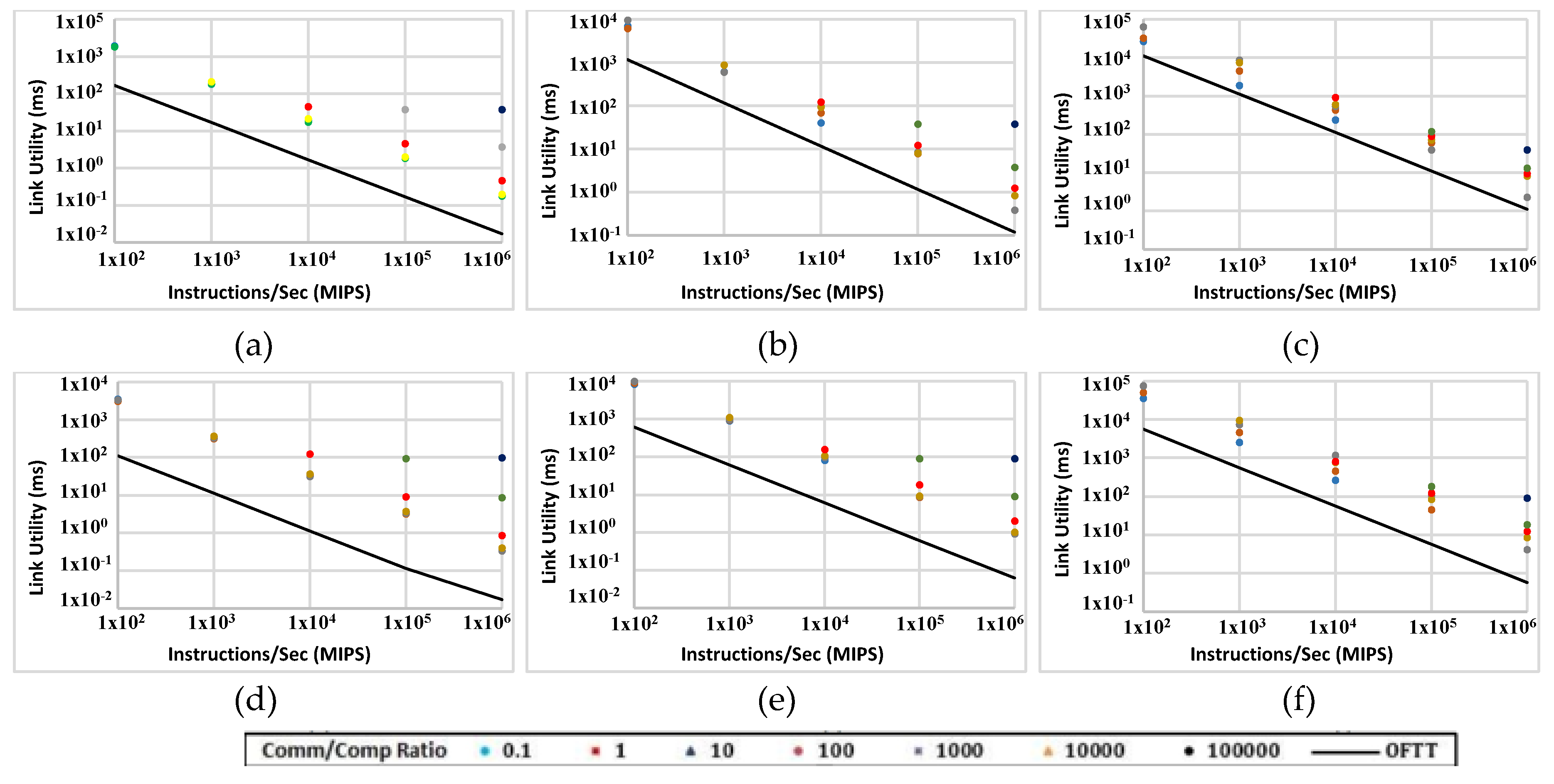
The same comparison is made for a direct 5D network (Figure 16). In most experiments, the gap between the ideal and actual values is even wider compared with the ABC network. This helps with identifying how much of the power consumed by the transceivers is used for real data. For most data points with both topologies and with all data sizes, the real data are responsible for just a little of the transmission power and time. A comparison between Figure 15 and Figure 16 indicates that ABC yields even better results than 5D topology in terms of the portion of transmission dedicated to real data.
This implies that the performance can be improved by adopting a more flexible task model and, more importantly, a more effective packet-switching mechanism. This is predictable because the overall latency in all store-and-forward packet-switching algorithms (like the one used in these experiments) increases as the number of hops increases. This suggests that a cut-through or wormhole packet-switching algorithm may have a chance to improve the performance of the network through a significant decrease in both overall transmission time and power consumption.
4. Conclusions and Future Work
Two topologies for a wireless interconnect network for a massively parallel computer (called A Ball Computer or the ‘ABC’) are presented in this paper. Considering the developments in wireless technologies during the past decade, they are close to meeting the criteria for such an application. However, this paper has shown that more improvements in transfer rate and, more importantly, in energy consumption are needed to be able to build a competitive real-world prototype of the ABC.
We have reviewed several works on mm-wave on-chip radio and showed that an energy consumption of 0.05 pJ/bit/cm has already been achieved, which means that a 20 Gb/s transceiver of this type will have an approximate power consumption of 1mW. These are promising numbers and the emergence of terahertz on-chip radio devices in the future will mean a further improvement in both data rates and power demands.
A 3D topology for the ABC concept is modelled in a simulation environment to perform experiments on the behaviour of the proposed platform under different situations. This paper has presented the performance analysis of the ABC based on processor and link utilisations. The link measurements are repeated with a simulated traditional 5D direct network (like IBM’s Blue Gene topology) to have a basis for comparison. The packet-switching algorithm used in the simulation has been under scrutiny using the simulation results.
The results have shown that for a given range of network parameters the performance of the ABC is comparable to (or sometimes even better than) a 5D network. The store-and-forward packet-switching algorithm used in the simulations is believed to contribute to the drop in performance in both the ABC and 5D topologies. Choosing a cut-through or especially a wormhole algorithm can improve the link efficiency. The link and processor performance are slightly reduced when the size of the network is increased from 1000 nodes to 2000, which implies that the FFT task model used in the simulations needs to be changed to let it use the full potential of a larger network.
The experiments have also shown that switching to very high transfer rates does not always lead to a meaningful improvement in the performance. In most cases the processor utility does not increase much, but levels out or even drops when switching from 100 Gb/s to 1 Tb/s. In addition, the link busy time is sometimes unchanged after switching to 1 Tb/s. This suggests that, at least with the current packet-switching mechanism and task model, there is no need to consider data rates over 100 Gb/s. In case of using another switching algorithm or task model, this assumption may not be valid anymore.
One of the paths for future work is to abandon the principle of having static nodes and let them have freedom of movement (at least to some extent). The self-autonomy given to the nodes turns them into an agent or robot rather than just processing nodes. This touches on the idea of swarm robotics /swarm computing. The wide range of possibilities in this path is very convincing. Agents (formerly referred to as nodes) can organise themselves to fit a given task. They can collaborate and coordinate based on the assigned task and even the geography and geometry they operate in. This also touches on areas like distributed control. The applications of such a system range from modelling biological systems to social systems, robust control systems, monitoring, rescue missions, urban life management and many more.
Despite the restrictions on current wireless technologies, the results have encouraged us to undertake more research in this field. A more efficient packet-switching algorithm is needed. Then it is possible to have a more detailed picture of the role of the original packet-switching algorithm in shaping the performance of the proposed network. The task model will be modified to avoid a drop in performance when the network expands. Also, the 4D ABC topology briefly introduced in this paper will be investigated further in the future. Building a prototype of the ABC in the real world is the final goal of this research.
Acknowledgments
The authors would like to thank EPSRC as this paper is based on research partially funded by the DAME (Distributed Aircraft Maintenance Environment) project supported by EPSRC (Engineering and Physical Sciences Research Council) (reference number: GR/R67668/01).
Author Contributions
The idea of Ball Computing was first suggested by Jim Austin. The 4D topology of ABC is proposed by Jim Austin. The 3D topology of ABC is a result of discussions among all the authors. The idea of using multiple frequencies was first proposed by Christopher Bailey and further developed by all the authors. The simulator used in this work is designed and developed by Amir Kamali under supervision of Jim Austin and Christopher Bailey. The experiments are conceived by Jim Austin, Christopher Bailey and Amir Kamali. Jim Austin authorised the use of White-Rose Grid to run the experiments. The experiments were designed and run by Amir Kamali. Jim Austin, Christopher Bailey and Amir kamali analysed the results. The graphs are made by Christopher Bailey and Amir Kamali. The first draft of the paper is written by Amir Kamali and is reviewed and edited by Christopher Bailey and Jim Austin.
Conflicts of Interest
The authors declare no conflict of interest.
References
- Moore, B.; Sellathamby, C.; Slupsky, S.; Iniewski, K. Chip to chip communications for terabit transmission rates. In Proceedings of the IEEE Asia Pacific Conference on Circuits and Systems (APCCAS), Macao, China, 30 November–3 December 2008. [Google Scholar]
- Mamei, M.; Menezes, R.; Tolksdorf, R.; Zambonelli, F. Case studies for self-organization in computer science. J. Syst. Archit. 2006, 52, 443–460. [Google Scholar] [CrossRef]
- Vassev, E.; Sterritt, R.; Rouff, C.; Hinchey, M. Swarm Technology at NASA: Building Resilient Systems. IT Prof. 2012, 14, 36–42. [Google Scholar] [CrossRef]
- Kamali, A.M.; Crispin-Bailey, C.; Austin, J. On advantages and limitations of 3D wireless grids as parallel platforms. In Proceedings of the International Conference on Selected Topics in Mobile and Wireless Networking (MoWNeT), Montreal, QC, Canada, 19–21 August 2013. [Google Scholar]
- Kamali, A.M.; Bailey, C.; Austin, J. Evaluating 3D wireless Grids as parallel platforms. Int. J. Ad Hoc Ubiquitous Comput. 2015, 19, 279–289, in press. [Google Scholar] [CrossRef]
- Hind, R. Feasibility Study on Implementing the Ball Computer. University of York, 1 June 2014. Available online: http://etheses.whiterose.ac.uk/id/eprint/4438 (accessed on 13 July 2015).
- Kamali Sarvestani, A.M. Evaluating Techniques for Wireless Interconnected 3D Processor Arrays. 26 March 2015. Available online: http://etheses.whiterose.ac.uk/8395/ (accessed on 31 March 2015).
- Aung, M.T.L.; Lim, E.; Yoshikawa, T.; Kim, T.T.-H. Design of Simultaneous Bi-Directional Transceivers Utilizing Capacitive Coupling for 3DICs in Face-to-Face Configuration. IEEE J. Emerg. Sel. Top. Circuits Syst. 2012, 2, 257–265. [Google Scholar] [CrossRef]
- Hopkins, D.; Chow, A.; Bosnyak, R.; Coates, B.; Ebergen, J.; Fairbanks, S.; Gainsley, J.; Ho, R.; Lexau, J.; Liu, F.; et al. Circuit Techniques to Enable 430Gb/s/mm2 Proximity Communication. In Proceedings of the IEEE International Solid-State Circuits Conference, San Fransisco, CA, USA, 11–15 Feburary 2007. [Google Scholar]
- Canegallo, R.; Perugini, L.; Pasini, A.; Innocenti, M.; Scandiuzzo, M.; Guerrieri, R.; Rolandi, P. System on Chip with 1.12mW-32Gb/s AC-Coupled 3D Memory Interface. In Proceedings of the IEEE Custom Intergrated Circuits Conference (CICC), Rome, Italy, 13–16 September 2009. [Google Scholar]
- Matsubara, T.; Hayashi, I.; Johari, A.H.; Kumaki, S.; Kohira, K.; Kuroda, T.; Ishikuro, H. An 0.5 V, 0.91 pJ/bit, 1.1 Gb/s/ch Transceiver in 65 nm CMOS for High-Speed Wireless Proximity Interface. In Proceedings of the IEEE Radio and Wireless Symposium (RWS), Phoenix, AZ, USA, 16–19 Janurary 2011. [Google Scholar]
- Miura, N.; Kasuga, K.; Saito, M.; Kuroda, T. An 8 Tb/s 1 pJ/b 0.8 mm2/Tb/s QDR Inductive-Coupling Interface Between 65 nm CMOS GPU and 0.1 μm DRAM. In Proceedings of the IEEE International Solid-State Circuits Conference, San Fransisco, CA, USA, 7–11 Feburary 2010. [Google Scholar]
- Lee, S.; Song, K.; Yoo, J.; Yoo, H.-J. A Low-Energy Inductive Coupling Transceiver With Cm-Range 50-Mbps Data Communication in Mobile Device Applications. IEEE J. Solid-State Circuits 2010, 45, 2366–2374. [Google Scholar] [CrossRef]
- Defrem, N.; Reynaert, P. A 120 GHz 10 Gb/s Phase-Modulating Transmitter in 65 nm LP CMOS. In Proceedings of the IEEE International Solid-State Circuits Conference, San Fransisco, CA, USA, 20–24 Feburary 2011. [Google Scholar]
- Katayama, K.; Motoyoshi, M.; Takano, K.; Ono, N.; Fujishima, M. 28 mW 10 Gbps Transmitter for 120 GHz ASK Transceiver. In Proceedings of the IEEE International Microwave Symposium, Montréal, QC, Canada, 17–22 June 2012. [Google Scholar]
- Hu, S.; Xiong, Y.-Z.; Zhang, B.; Wang, L.; Lim, T.-G.; Je, M.; Madihian, M. A SiGe BiCMOS Transmitter/Receiver Chipset with On-Chip SIW Antennas for Terahertz Applications. IEEE J. Solid-State Circuits 2012, 47, 2654–2664. [Google Scholar] [CrossRef]
- Ishigaki, K.; Shiraishi, M.; Suzuki, S.; Asada, M.; Nishiyama, N.; Arai, S. Direct intensity modulation and wireless data transmission characteristics of terahertz-oscillating resonant tunnelling diodes. Electron. Lett. 2012, 48, 582–583. [Google Scholar] [CrossRef]
- Foulon, S.; Pruvost, S.; Loyez, C.; Rolland, N.; Avramovic, V. A 10 GBits/s 2.1 pJ/bit OOK demodulator at 60 GHz for chip-to-chip wireless communication. In Proceedings of the IEEE Radio and Wireless Symposium, Santa Clara, CA, USA, 15–18 Janurary 2012. [Google Scholar]
- Miyashita, D.; Agawa, K.; Kajihara, H.; Sami, K.; Iwanaga, M.; Ogasawara, Y.; Ito, T.; Kurose, D.; Koide, N.; Hashimoto, T.; et al. A-70dBm-Sensitivity 522 Mbps 0.19 nJ/bit-TX 0.43 nJ/bit-RX Transceiver for TransferJet™ SoC in 65 nm CMOS. In Proceedings of the IEEE Symposium on VLSI Circuits, Honolulu, HI, USA, 13–15 June 2012. [Google Scholar]
- Kanda, K.; Antono, D.D.; Ishida, K.; Kawaguchi, H.; Kuroda, T.; Sakurai, T. 1.27 Gb/s/pin 3 mW/pin Wireless Superconnect (WSC) Interface Scheme. In Proceedings of the IEEE International Solid-State Circuits Conference, San Francisco, CA, USA, 13 Feburary 2003. [Google Scholar]
- Drost, R.J.; Hopkins, R.D.; Ho, R.; Sutherland, I.E. Proximity Communication. IEEE J. Solid-State Circuits 2004, 39, 1529–1535. [Google Scholar] [CrossRef]
- Fazzi, A.; Magagni, L.; Mirandola, M.; Canegallo, R.; Schmitz, S.; Guerrieri, R. A 0.14 mW/Gbps High-Density Capacitive Interface for 3D System Integration. In Proceedings of the IEEE Custom Integrated Circuits Conference, San Jose, CA, USA, 21 September 2005. [Google Scholar]
- Canegallo, R.; Fazzi, A.; Ciccarelli, L.; Magagni, L.; Natali, F.; Rolandi, P.; Jung, E.; Di Cioccio, L.; Guerrieri, R. 3D Capacitive Interconnections for High Speed Interchip Communication. In Proceedings of the IEEE Custom Intergrated Circuits Conference (CICC), San Jose, CA, USA, 16–19 September 2007. [Google Scholar]
- Miura, N.; Mizoguchi, D.; Binti Yusof, Y.; Sakurai, T.; Kuroda, T. Analysis and Design of Transceiver Circuit and Inductor Layout for Inductive Inter-chip Wireless Superconnect. In Proceedings of the Symposium on VLSl Circuit, Honolulu, HI, USA, 17–19 June 2004. [Google Scholar]
- Sasaki, M.; Iwata, A. A 0.95 mW/1.0 Gbps Spiral-Inductor Based Wireless Chip-Interconnect with Asynchronous Communication Scheme. In Proceedings of the IEEE Symposium on VLSI Circuits, Kyoto, Japan, 16–18 June 2005. [Google Scholar]
- Miura, N.; Ishikuro, H.; Sakurai, T.; Kuroda, T. A 0.14 pJ/b Inductive-Coupling Inter-Chip Data Transceiver with Digitaly-Controlled Precise Pulse Shaping. In Proceedings of the IEEE International Solid-State Circuits Conference, San Francisco, CA, USA, 11–15 Feburary 2007. [Google Scholar]
- Lee, S.; Yoo, J.; Yoo, H.-J. A 200 Mbps 0.02 nJ/b dual-mode inductive coupling transceiver for cm-range interconnection. In Proceedings of the IEEE International Symposium on Circuits and Systems (ISCAS), Seattle, WA, USA, 18–21 May 2008. [Google Scholar]
- Lee, S.; Yoo, J.; Song, K.; Yoo, H.-J. A 1.3 pJ/b Inductive Coupling Transceiver with Adaptive Gain Control for Cm-range 50 Mbps Data Communication. In Proceedings of the IEEE Asian Solid-State Circuits Conference, Taipei, Taiwan, 16–18 November 2009. [Google Scholar]
- Terada, T.; Yoshizumi, S.; Sanada, Y.; Kuroda, T. Transceiver Circuits for pulse-based ultra-wideband. In Proceedings of the International Symposium on Circuits and Systems (ISCAS), Vancouver, BC, Canada, 23–26 May 2004. [Google Scholar]
- Terada, T.; Yoshizumi, S.; Sanada, Y.; Kuroda, T. A CMOS impulse radio ultra-wideband transceiver for 1 Mb/s data communications and ±2.5 cm range findings. In Proceedings of the Symposium on VLSI Circuits, Kyoto, Japan, 16–18 June 2005. [Google Scholar]
- Reynolds, S.K.; Floyd, B.A.; Pfeiffer, U.R.; Beukema, T.; Grzyb, J.; Haymes, C.; Gaucher, B.; Soyuer, M. A Silicon 60-GHz Receiver and Transmitter Chipset for Broadband Communications. IEEE J. Solid-State Circuits 2006, 41, 2820–2831. [Google Scholar] [CrossRef]
- Sarkar, S.; Laskar, J. A Single-Chip 25 pJ/bit Multi-Gigabit 60 GHz Receiver Module. In Proceedings of the IEEE/MTT-S International Microwave Symposium, Honolulu, HI, USA, 3–8 June 2007. [Google Scholar]
- Tomkins, A.; Aroca, R.A.; Yamamoto, T.; Nicolson, S.T.; Doi, Y.; Voinigescu, S.P. A Zero-IF 60 GHz Transceiver in 65 nm CMOS with > 3.5 Gb/s Links. In Proceedings of the IEEE CustomIntegrated Circuits Conference, San Jose, CA, USA, 21–24 September 2008. [Google Scholar]
- Marcu, C.; Chowdhury, D.; Thakkar, C.; Kong, L.-K.; Tabesh, M.; Park, J.-D.; Wang, Y.; Afshar, B.; Gupta, A.; Arbabian, A.; et al. A 90 nm CMOS Low-Power 60 GHz Transceiver with Integrated Baseband Circuitry. IEEE J. Solid-State Circuits 2009, 44, 3434–3447. [Google Scholar] [CrossRef]
- Cohen, E.; Jakobson, C.; Ravid, S.; Ritter, D. A thirty two element phased-array transceiver at 60 GHz with RF-IF conversion block in 90 nm flip chip CMOS process. In Proceedings of the IEEE Radio Frequency Integrated Circuits Symposium, Anaheim, CA, USA, 23–25 May 2010. [Google Scholar]
- Okada, K.; Li, N.; Matsushita, K.; Bunsen, K.; Murakami, R.; Musa, A.; Sato, T.; Asada, H.; Takayama, N.; Ito, S.; et al. A 60-GHz 16QAM/8PSK/QPSK/BPSK Direct-Conversion Transceiver for IEEE802.15.3c. IEEE J. Solid-State Circuits 2011, 46, 2988–3004. [Google Scholar] [CrossRef]
- Thakkar, C.; Kong, L.; Jung, K.; Frappé, A.; Alon, E. A 10 Gb/s 45 mW Adaptive 60 GHz Baseband in 65 nm CMOS. IEEE J. Solid-State Circuits 2012, 47, 952–968. [Google Scholar] [CrossRef]
- Deb, S.; Ganguly, A.; Chang, K.; Pande, P.; Belzer, B.; Heo, D. Enhancing Performance of Network-on-Chip Architectures with Millimeter-Wave Wireless Interconnects. In Proceedings of the 21st IEEE International Conference on Application-specific Systems Architectures and Processors (ASAP), Rennes, France, 7–9 July 2010. [Google Scholar]
- Kawasaki, K.; Akiyama, Y.; Komori, K.; Uno, M.; Takeuchi, H.; Itagaki, T.; Hino, Y.; Kawasaki, Y.; Ito, K.; Hajimiri, A. A Millimeter-Wave Intra-Connect Solution. IEEE J. Solid-State Circuits 2010, 45, 2655–2666. [Google Scholar] [CrossRef]
- Yu, X.; Sah, S.P.; Deb, S.; Pande, P.P.; Belzer, B.; Heo, D. A Wideband Body-Enabled Millimeter-Wave Transceiver for Wireless Network-on-Chip. In Proceedings of the IEEE 54th International Midwest Symposium on Circuits and Systems (MWSCAS), Seoul, Korea, 7–10 August 2011. [Google Scholar]
- Fukuda, S.; Hino, Y.; Ohashi, S.; Takeda, T.; Yamagishi, H.; Shinke, S.; Komori, K.; Uno, M.; Akiyama, Y.; Kawasaki, K.; et al. A 12.5+12.5 Gb/s Full-Duplex Plastic Waveguide Interconnect. IEEE J. Solid-State Circuits 2011, 46, 3113–3125. [Google Scholar] [CrossRef]
- Tanaka, Y.; Hino, Y.; Okada, Y.; Takeda, T.; Ohashi, S.; Yamagishi, H.; Kawasaki, K.; Hajimiri, A. A Versatile Multi-Modality Serial Link. In Proceedings of the IEEE International Solid-State Circuits Conference, San Fransisco, CA, USA, 19–23 Feburary 2012. [Google Scholar]
- Byeon, C.W.; Yoon, C.H.; Park, C.S. A 67-mW 10.7-Gb/s 60-GHz OOK CMOS Transceiver for Short-Range Wireless Communications. IEEE Trans. Microw. Theory Tech. 2013, 61, 3391–3401. [Google Scholar] [CrossRef]
- Yu, X.; Sah, S.P.; Rashtian, H.; Mirabbasi, S.; Pande, P.P.; Heo, D. A 1.2-pJ/bit 16-Gb/s 60-GHz OOK Transmitter in 65-nm CMOS for Wireless Network-On-Chip. IEEE Trans. Microw. Theory Tech. 2014, 62, 2357–2369. [Google Scholar] [CrossRef]
- Nakajima, K.; Maruyama, A.; Kohtani, M.; Sugiura, T.; Otobe, E.; Lee, J.; Cho, S.; Kwak, K.; Lee, J.; Yoshimasu, T.; et al. 23 Gbps 9.4 pJ/bit 80/100 GHz band CMOS transceiver with on-board antenna for short-range communication. In Proceedings of the Solid-State Circuits Conference (A-SSCC), KaoHsiung, Taiwan, 10–12 November 2014. [Google Scholar]
- Yu, X.; Rashtian, H.; Mirabbasi, S.; Pande, P.P.; Heo, D. An 18.7-Gb/s 60-GHz OOK Demodulator in 65-nm CMOS for Wireless Network-on-Chip. IEEE Trans. Circuits Syst. I Regul. Pap. 2015, 62, 799–806. [Google Scholar] [CrossRef]
- Lee, H.J.; Lee, J.G.; Lee, C.J.; Jang, T.H.; Kim, H.J.; Park, C.S. High-speed and low-power OOK CMOS transmitter and receiver for wireless chip-to-chip communication. In Proceedings of the 2015 IEEE MTT-S International Microwave Workshop Series on Advanced Materials and Processes for RF and THz Applications (IMWS-AMP), Suzhou, China, 1–3 July 2015. [Google Scholar]
- Rabaey, J. Short-Distance Wireless and Its Opportunities. In Wireless Technologies: Circuits, Systems and Devices; CRC Press: Boca Raton, FL, USA, 2007. [Google Scholar]
- Intel. Switches, What Are Forwarding Modes and How Do They Work? 17 April 2014. Available online: http://www.intel.com/support/express/switches/sb/cs-014410.htm (accessed on 1 April 2015).
- Gauss, C.F. Intersuchungen über die Eigenschaften der Positiven Ternären Quadratischen Formen Usw. Göttingsche Gelehrte Anzeigen 1831, 9, 1065. [Google Scholar]
Figure 1.
Normalised energy needed to send a bit over (a) 1 μm using capacitive coupling; (b) 1 μm using Inductive coupling; (c) 1 mm using radio waves.
Figure 1.
Normalised energy needed to send a bit over (a) 1 μm using capacitive coupling; (b) 1 μm using Inductive coupling; (c) 1 mm using radio waves.
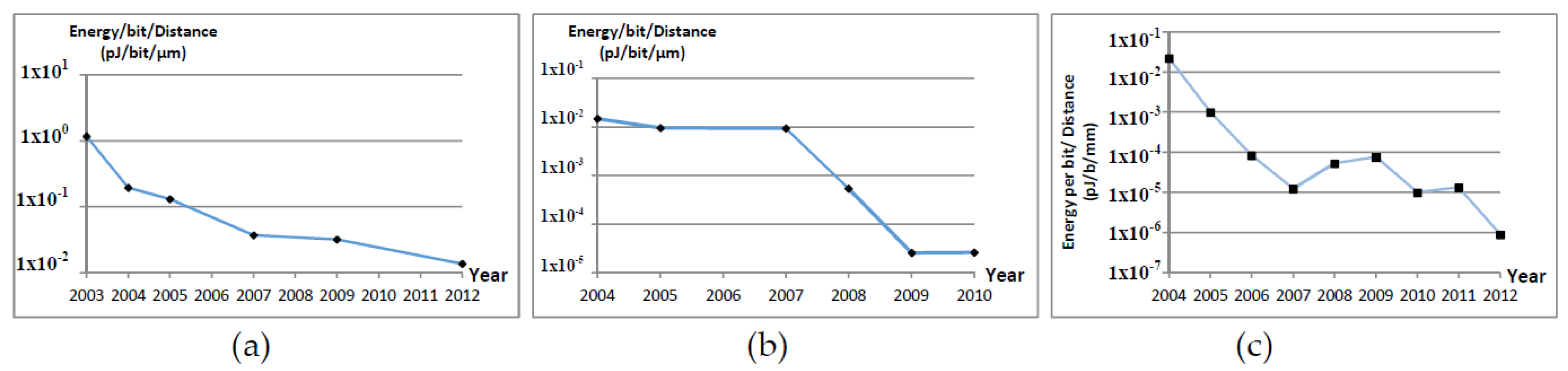
Figure 2.
Data rate, distance and power consumption criteria applied to reviewed wireless technologies; (a) Data rate vs. distance; (b) data rate vs. power consumption; (c) power consumption vs. distance. Shadowed areas cover the technologies that satisfy the criteria.
Figure 2.
Data rate, distance and power consumption criteria applied to reviewed wireless technologies; (a) Data rate vs. distance; (b) data rate vs. power consumption; (c) power consumption vs. distance. Shadowed areas cover the technologies that satisfy the criteria.
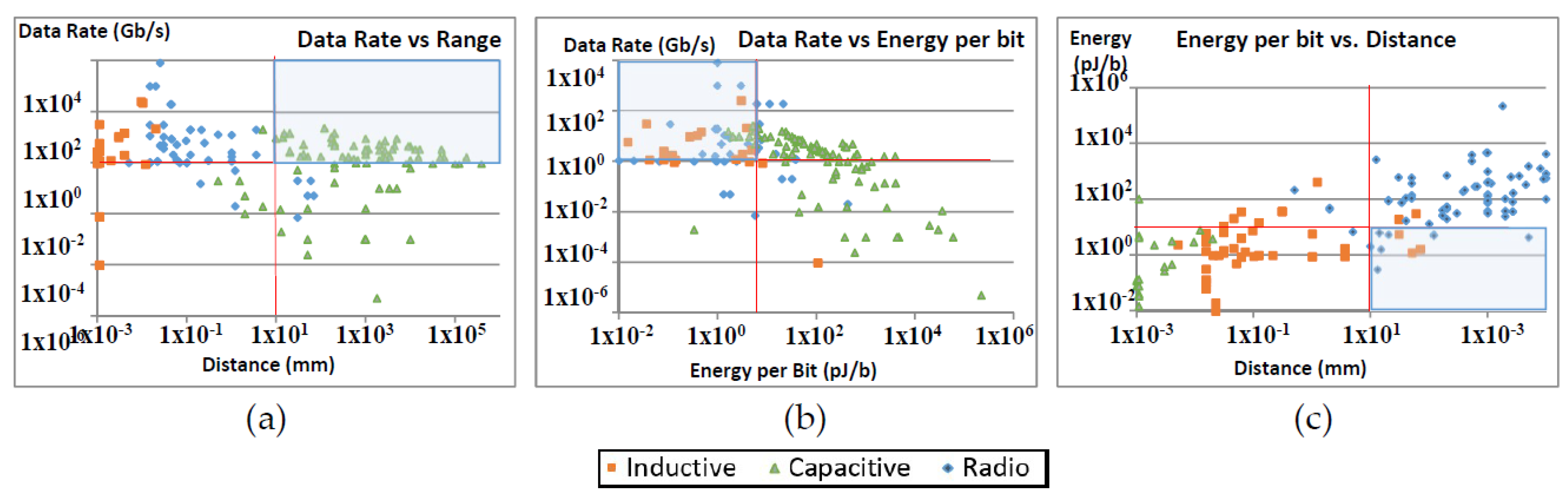
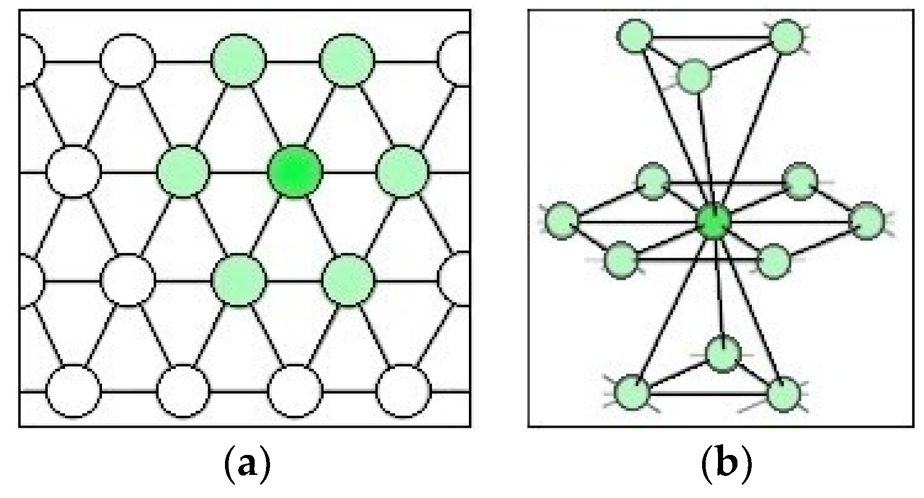
Figure 3.
The topology of a ball computer in (a) 2D and (b) 3D.

Figure 4.
The process of forming a zone. The top three images show three neighbour nodes and their radio ranges. The bottom left image shows the overlap of those ranges which makes a common pink region in middle bottom image. The channel inclusion (green) and exclusion (red) areas are defined in bottom left image.
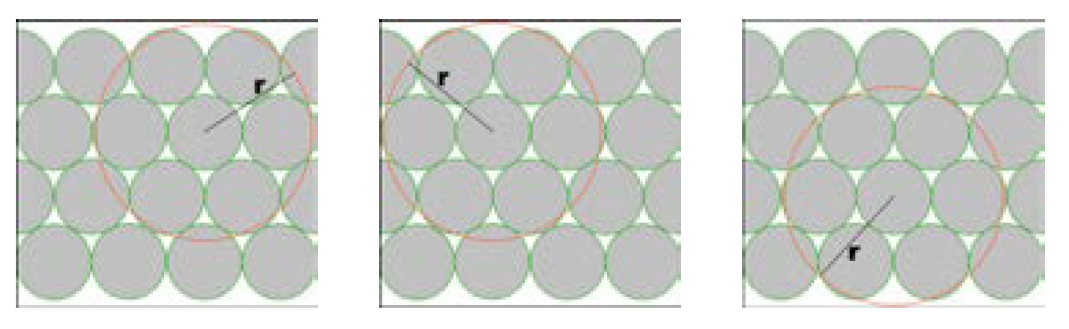
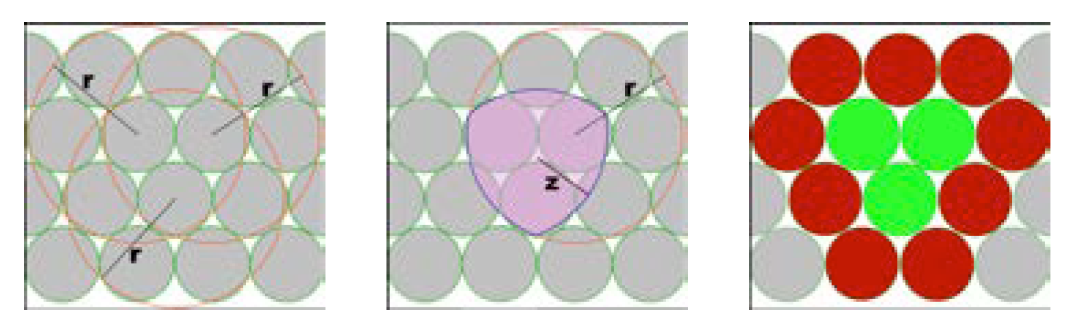
Figure 5.
A 3D grid of nodes and the partitions around a node (Z1 to Z8).

Figure 6.
The maximum number of hops in Blue Gene/Q compared with 3D wireless hexagonal grids (d is the diameter of each ball).
Figure 6.
The maximum number of hops in Blue Gene/Q compared with 3D wireless hexagonal grids (d is the diameter of each ball).

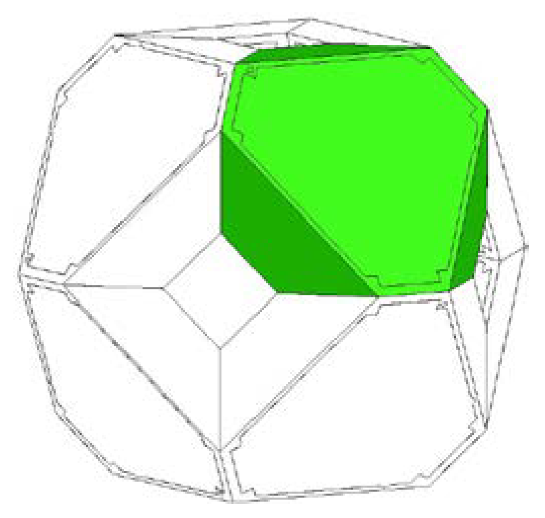
Figure 7.
A ball in a 4D topology consists of eight modules. Each module (green) has two processors and six transceivers (dark green).
Figure 7.
A ball in a 4D topology consists of eight modules. Each module (green) has two processors and six transceivers (dark green).

Figure 8.
Inside a ball. Two separate cubes of processors are merged and connected to form a ball in a 4D fashion.
Figure 8.
Inside a ball. Two separate cubes of processors are merged and connected to form a ball in a 4D fashion.
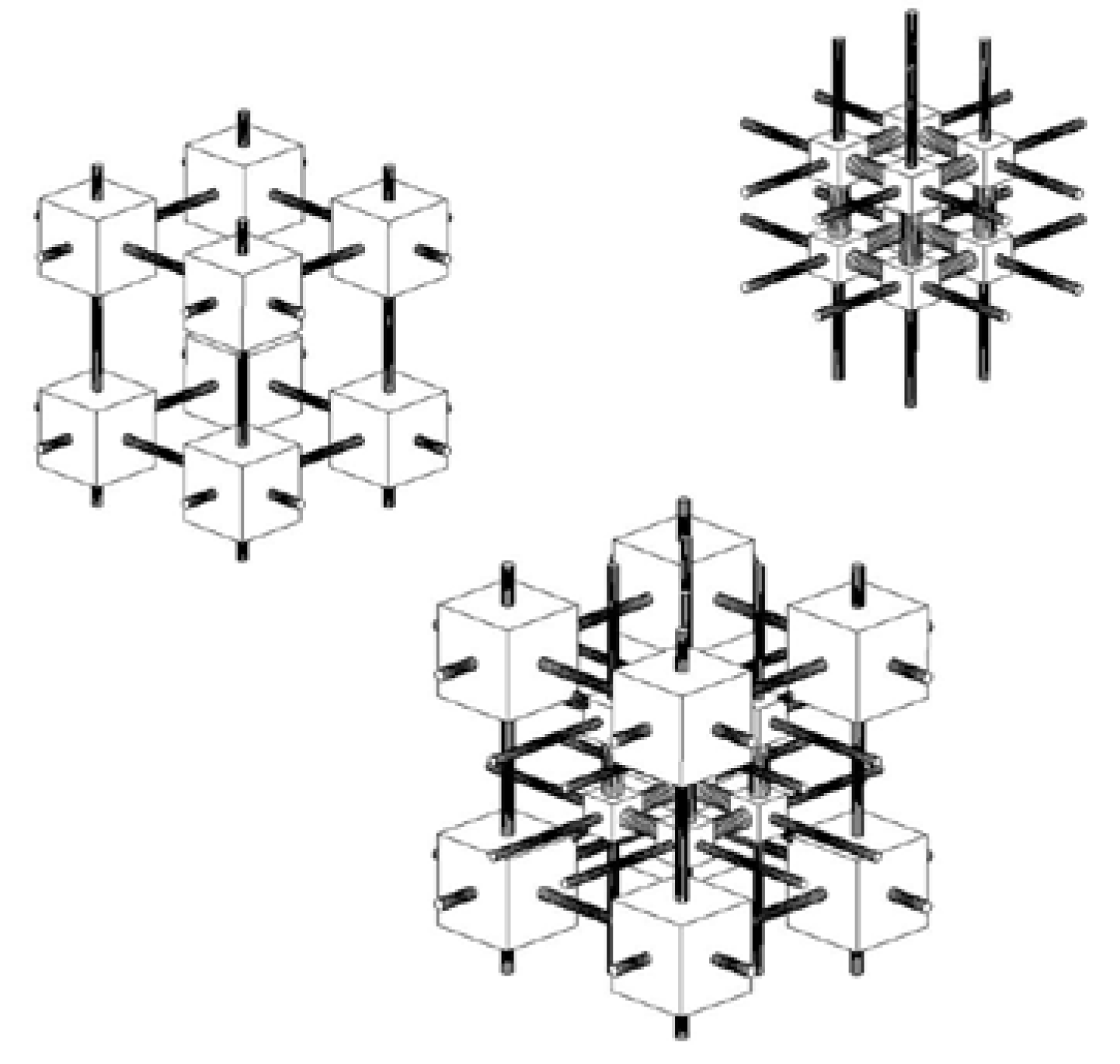
Figure 9.
Processor utility for FFTTM on ABC with two sizes: 1000 nodes (a,c,e) and 2000 nodes (b,d,f). Data sizes are 100 KB (a,b), 1 MB (c,d) and 10 MB (e,f). Blue, red, green, orange and black graphs represent the computational ability of 0.01, 0.1, 1, 10 and 100 GIPS respectively.
Figure 9.
Processor utility for FFTTM on ABC with two sizes: 1000 nodes (a,c,e) and 2000 nodes (b,d,f). Data sizes are 100 KB (a,b), 1 MB (c,d) and 10 MB (e,f). Blue, red, green, orange and black graphs represent the computational ability of 0.01, 0.1, 1, 10 and 100 GIPS respectively.

Figure 10.
Processor utility for FFTTM on a 5D grid with two sizes: 1000 nodes (a,c,e) and 2000 nodes (b,d,f). Data sizes are 100 KB (a,b), 1 MB (c,d) and 10 MB (e,f). Blue, red, green, orange and black graphs represent computational ability of 0.01, 0.1, 1, 10 and 100 GIPS respectively.
Figure 10.
Processor utility for FFTTM on a 5D grid with two sizes: 1000 nodes (a,c,e) and 2000 nodes (b,d,f). Data sizes are 100 KB (a,b), 1 MB (c,d) and 10 MB (e,f). Blue, red, green, orange and black graphs represent computational ability of 0.01, 0.1, 1, 10 and 100 GIPS respectively.
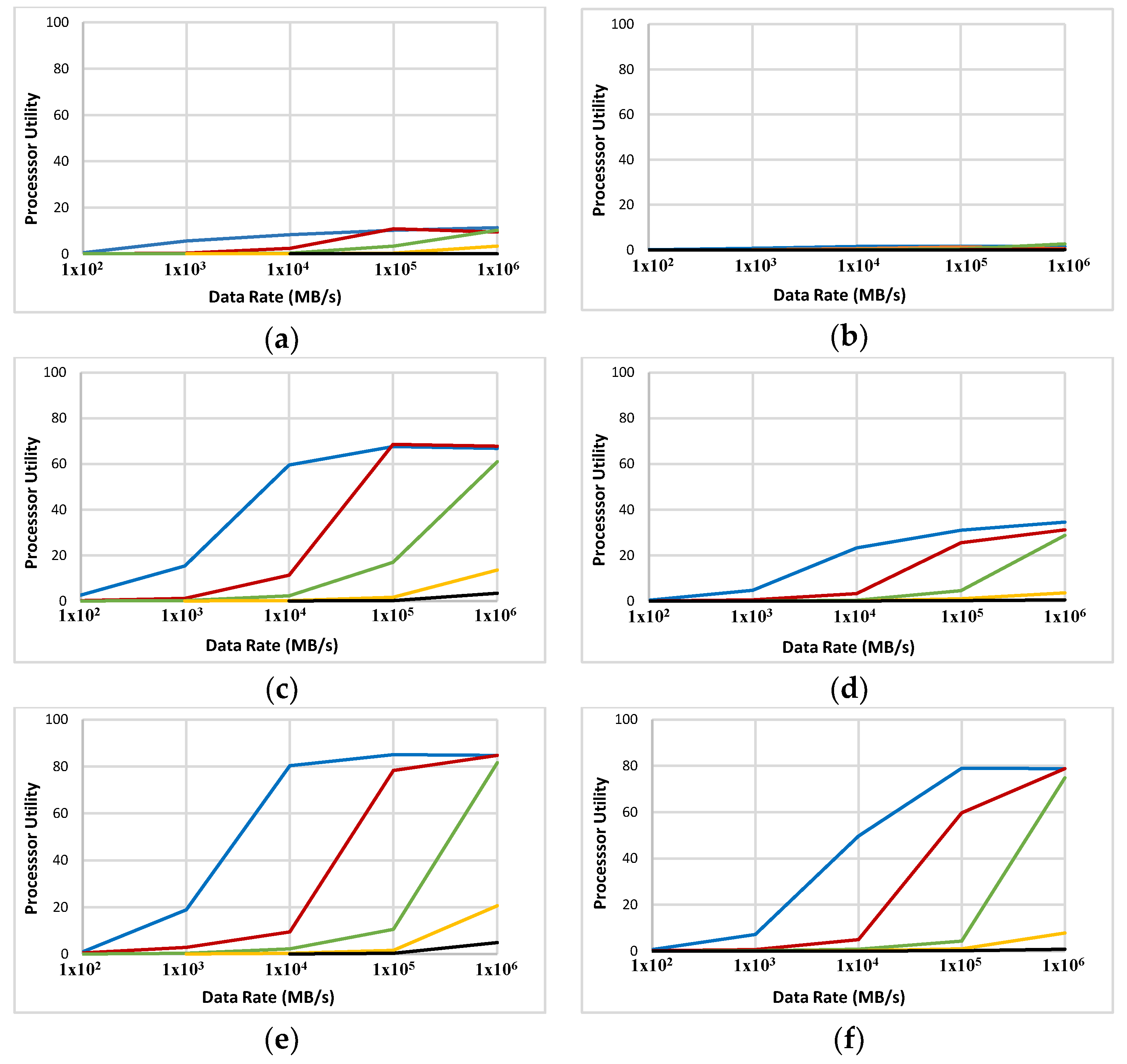
Figure 11.
Link busy time (OLBT in ms) for FFTTM on ABC with two sizes: 1000 nodes (a,c,e) and 2000 nodes (b,d,f). Data sizes are 100 KB (a,b), 1 MB (c,d) and 10 MB (e,f). Blue, red, green, orange and black graphs represent computational ability of 0.01, 0.1, 1, 10 and 100 GIPS respectively.
Figure 11.
Link busy time (OLBT in ms) for FFTTM on ABC with two sizes: 1000 nodes (a,c,e) and 2000 nodes (b,d,f). Data sizes are 100 KB (a,b), 1 MB (c,d) and 10 MB (e,f). Blue, red, green, orange and black graphs represent computational ability of 0.01, 0.1, 1, 10 and 100 GIPS respectively.
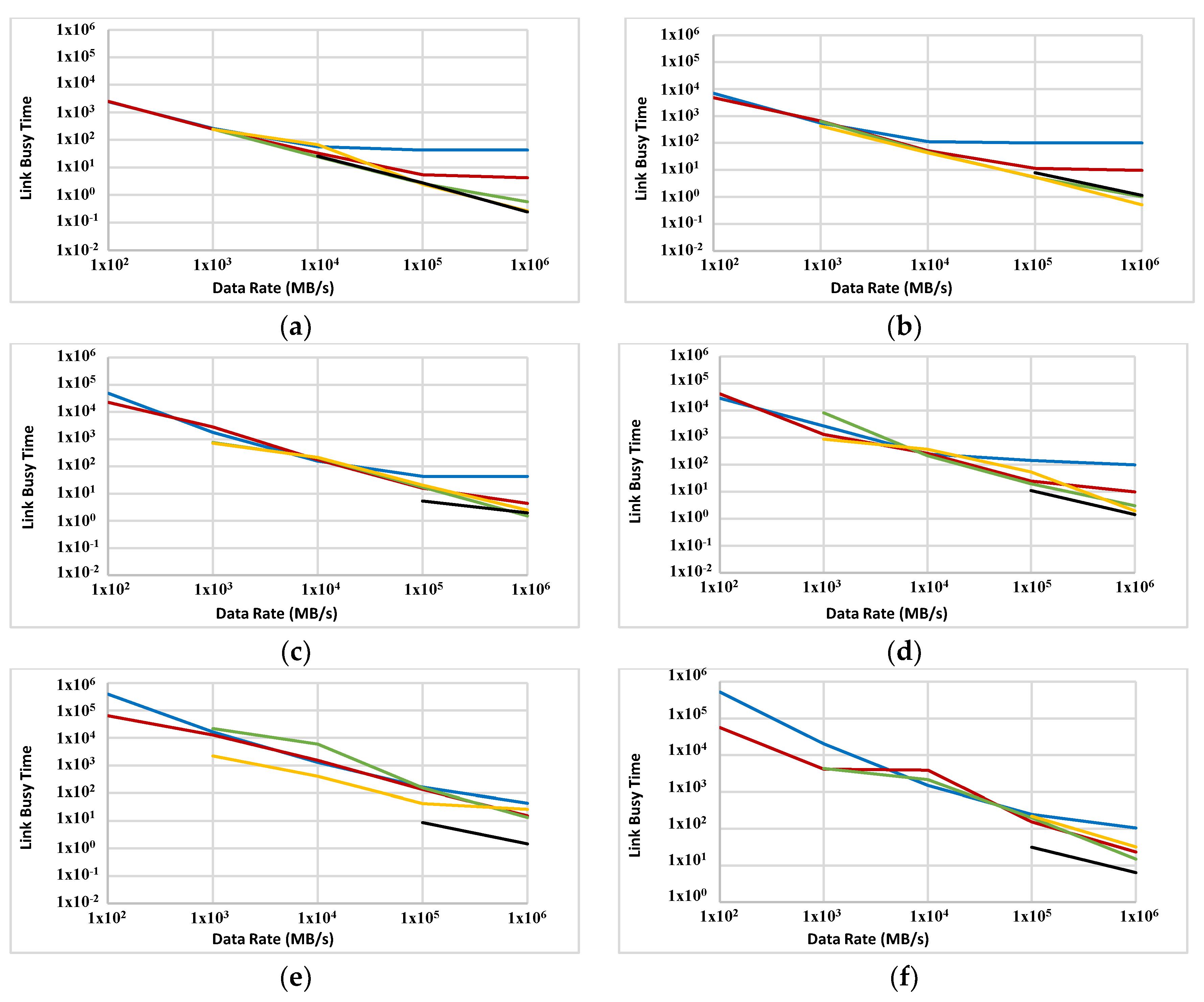
Figure 12.
Link busy time (OLBT in ms) for FFTTM on a 5D grid with two sizes: 1000 nodes (a,c,e) and 2000 nodes (b,d,f). Data sizes are 100 KB (a,b), 1 MB (c,d) and 10 MB (e,f). Blue, red, green, orange and black graphs represent computational ability of 0.01, 0.1, 1, 10 and 100 GIPS respectively.
Figure 12.
Link busy time (OLBT in ms) for FFTTM on a 5D grid with two sizes: 1000 nodes (a,c,e) and 2000 nodes (b,d,f). Data sizes are 100 KB (a,b), 1 MB (c,d) and 10 MB (e,f). Blue, red, green, orange and black graphs represent computational ability of 0.01, 0.1, 1, 10 and 100 GIPS respectively.
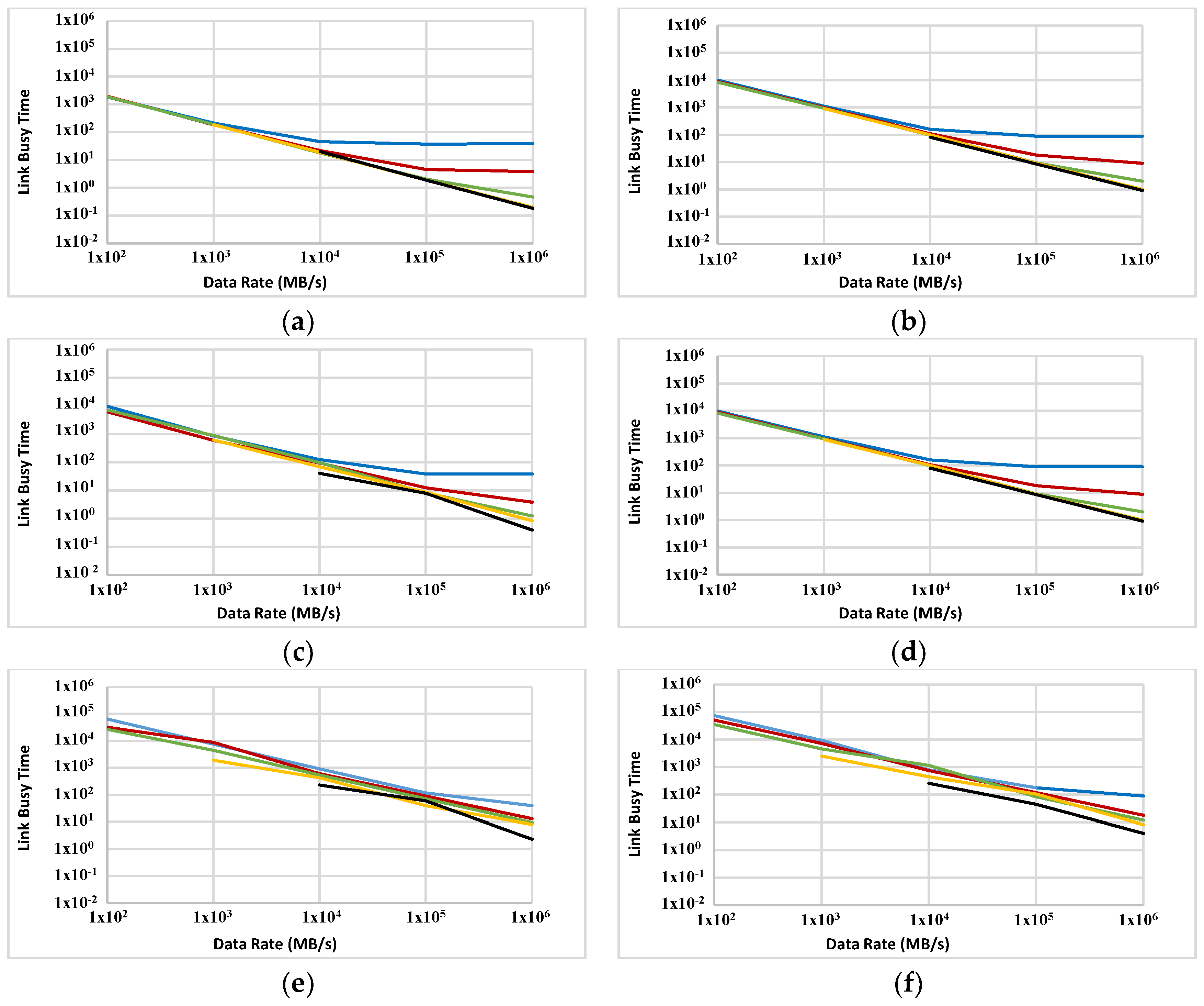
Figure 13.
Link wait time (OLWT in ms) for FFTTM on ABC with two sizes: 1000 nodes (a,c,e) and 2000 nodes (b,d,f). Data sizes are 100 KB (a,b), 1 MB (c,d) and 10 MB (e,f). Blue, red, green, orange and black graphs represent computational ability of 0.01, 0.1, 1, 10 and 100 GIPS, respectively.
Figure 13.
Link wait time (OLWT in ms) for FFTTM on ABC with two sizes: 1000 nodes (a,c,e) and 2000 nodes (b,d,f). Data sizes are 100 KB (a,b), 1 MB (c,d) and 10 MB (e,f). Blue, red, green, orange and black graphs represent computational ability of 0.01, 0.1, 1, 10 and 100 GIPS, respectively.
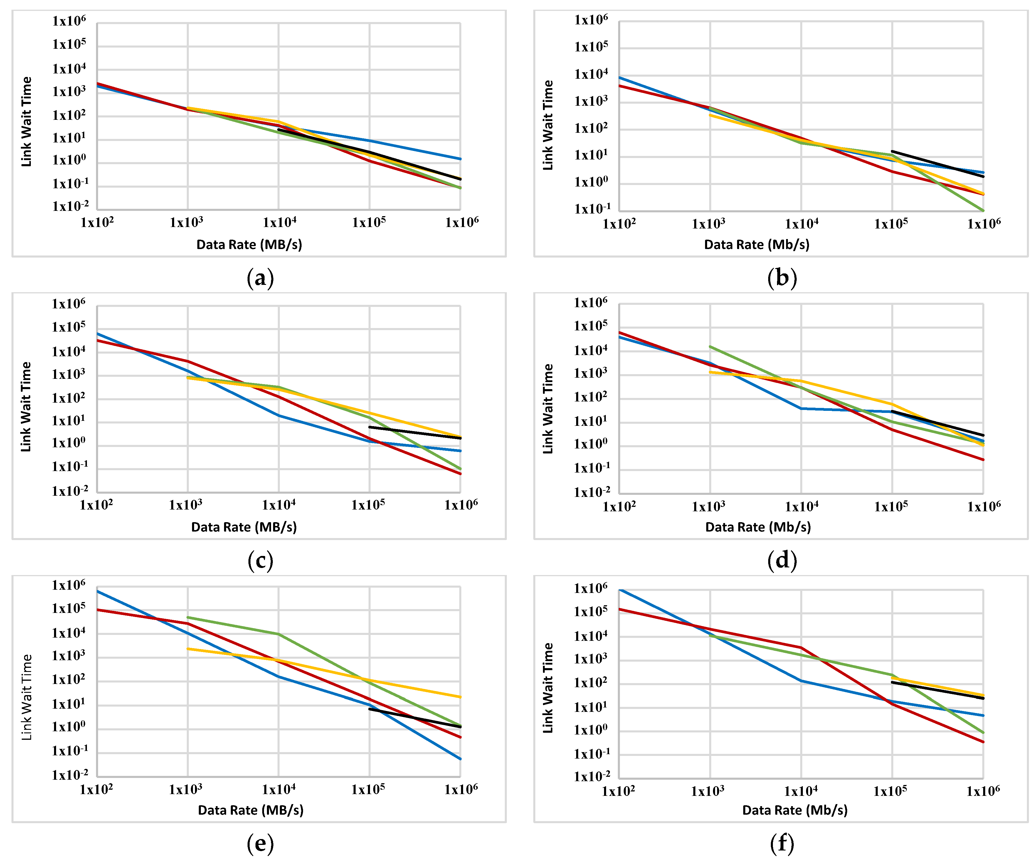
Figure 14.
Link wait time (OLWT in ms) for FFTTM on a 5D grid with two sizes: 1000 nodes (a,c,e) and 2000 nodes (b,d,f). Data sizes are 100 KB (a,b), 1 MB (c,d) and 10 MB (e,f). Blue, red, green, orange and black graphs represent computational ability of 0.01, 0.1, 1, 10 and 100 GIPS, respectively.
Figure 14.
Link wait time (OLWT in ms) for FFTTM on a 5D grid with two sizes: 1000 nodes (a,c,e) and 2000 nodes (b,d,f). Data sizes are 100 KB (a,b), 1 MB (c,d) and 10 MB (e,f). Blue, red, green, orange and black graphs represent computational ability of 0.01, 0.1, 1, 10 and 100 GIPS, respectively.

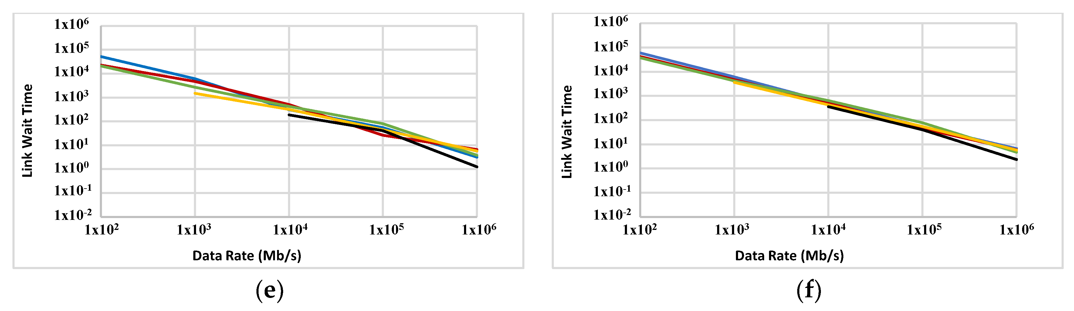
Figure 15.
Link busy time when comm/comp ratio varies between 0.1 and 100,000 in ABC with two sizes: 1000 nodes (a,b,c) and 2000 nodes (d,e,f) running FFTTM. Data sizes are 100 KB (a,d), 1 MB (b,e) and 10 MB (c,f).
Figure 15.
Link busy time when comm/comp ratio varies between 0.1 and 100,000 in ABC with two sizes: 1000 nodes (a,b,c) and 2000 nodes (d,e,f) running FFTTM. Data sizes are 100 KB (a,d), 1 MB (b,e) and 10 MB (c,f).
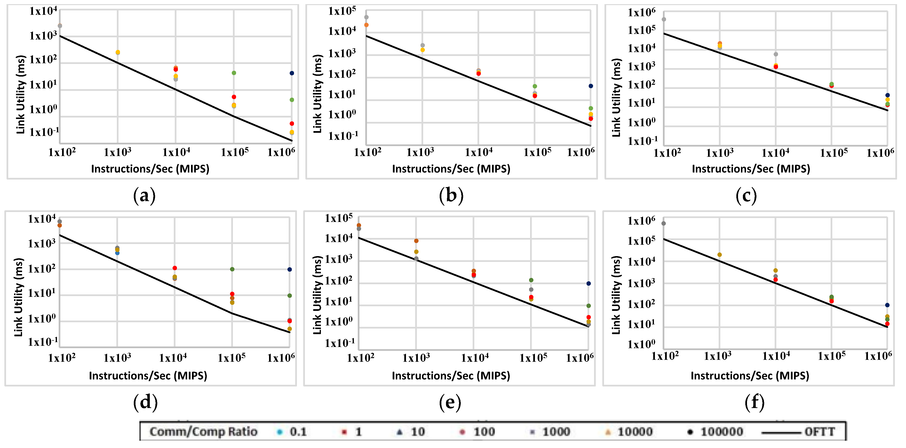
Figure 16.
Link busy time when comm/comp ratio varies between 0.1 and 100,000 in a 5D grid with two sizes: 1000 nodes (a,b,c) and 2000 nodes (d,e,f) running FFTTM. Data sizes are 100 KB (a,d), 1 MB (b,e) and 10 MB (c,f).
Figure 16.
Link busy time when comm/comp ratio varies between 0.1 and 100,000 in a 5D grid with two sizes: 1000 nodes (a,b,c) and 2000 nodes (d,e,f) running FFTTM. Data sizes are 100 KB (a,d), 1 MB (b,e) and 10 MB (c,f).

Table 1.
Wireless technologies for a 3D wireless grid.
| Ref. | Data Rate (Gb/s) | Range (mm) | Power (mW) | Energy/Bit (pJ/b) | Energy/Bit/Dist (pJ/b/mm) |
|---|---|---|---|---|---|
| [38] | 16 | 20 | 90 | 5.63 | 0.0141 |
| [39] | 11 | 14 | 70 | 6.4 | 0.0327 |
| [40] | 16 | 15 | 26.7 | 1.67 | 0.0074 |
| [41] | 25 | 120 | 140 | 5.6 | 0.0004 |
| [18] | 10 | 10 | 21 | 2.1 | 0.021 |
| [42] | 26 | 120 | 137 | 5.27 | 0.0004 |
| [42] | 20 | 5 | 137 | 5.85 | 0.234 |
| [43] | 10.7 | 100 | 67 | 6.26 | 0.0006 |
| [44] | 16 | 20 | 19 | 1.2 | 0.003 |
| [45] | 23 | 100 | 216 | 9.4 | 0.0009 |
| [46] | 18.7 | 20 | 4.6 | 0.25 | 0.0006 |
| [47] | 12 | 12 | 64 | 4.5 | 0.0313 |
© 2018 by the authors. Licensee MDPI, Basel, Switzerland. This article is an open access article distributed under the terms and conditions of the Creative Commons Attribution (CC BY) license (http://creativecommons.org/licenses/by/4.0/).
Share and Cite
MDPI and ACS Style
Kamali Sarvestani, A.M.; Bailey, C.; Austin, J. Performance Analysis of a 3D Wireless Massively Parallel Computer. J. Sens. Actuator Netw. 2018, 7, 18. https://doi.org/10.3390/jsan7020018
AMA Style
Kamali Sarvestani AM, Bailey C, Austin J. Performance Analysis of a 3D Wireless Massively Parallel Computer. Journal of Sensor and Actuator Networks. 2018; 7(2):18. https://doi.org/10.3390/jsan7020018
Chicago/Turabian StyleKamali Sarvestani, Amir Mansoor, Christopher Bailey, and Jim Austin. 2018. "Performance Analysis of a 3D Wireless Massively Parallel Computer" Journal of Sensor and Actuator Networks 7, no. 2: 18. https://doi.org/10.3390/jsan7020018
Note that from the first issue of 2016, this journal uses article numbers instead of page numbers. See further details here.