DC Model Cable under Polarity Inversion and Thermal Gradient: Build-Up of Design-Related Space Charge


1
PT. PLN (Persero) Jalan Trunojoyo, Blok M I/135, Jakarta 12160, Indonesia
2
Electrical Engineering Department, Electric Power University, 235 Hoang Quoc Viet, Hanoi 10000, Vietnam
3
Laboratory on Plasma and Conversion of Energy (LAPLACE), Université de Toulouse, CNRS, INPT, UPS, Bat 3R3, 118, route de Narbonne, Toulouse 31062, France
4
School of Electrical Engineering and Informatics, Bandung Institute of Technology, Jalan Ganesha, 10, Bandung 40132, Indonesia
*
Author to whom correspondence should be addressed.
Technologies 2017, 5(3), 46; https://doi.org/10.3390/technologies5030046
Submission received: 5 June 2017
/
Revised: 13 July 2017
/
Accepted: 13 July 2017
/
Published: 17 July 2017
(This article belongs to the Section Innovations in Materials Processing)
Abstract
:In the field of energy transport, High-Voltage DC (HVDC) technologies are booming at present due to the more flexible power converter solutions along with needs to bring electrical energy from distributed production areas to consumption sites and to strengthen large-scale energy networks. These developments go with challenges in qualifying insulating materials embedded in those systems and in the design of insulations relying on stress distribution. Our purpose in this communication is to illustrate how far the field distribution in DC insulation systems can be anticipated based on conductivity data gathered as a function of temperature and electric field. Transient currents and conductivity estimates as a function of temperature and field were recorded on miniaturized HVDC power cables with construction of 1.5 mm thick crosslinked polyethylene (XLPE) insulation. Outputs of the conductivity model are compared to measured field distributions using space charge measurements techniques. It is shown that some features of the field distribution on model cables put under thermal gradient can be anticipated based on conductivity data. However, space charge build-up can induce substantial electric field strengthening when materials are not well controlled.
1. Introduction
For energy transport purposes, the field of High-Voltage Direct Current (HVDC) technologies is booming at present due to the more flexible power converter solutions along with needs to bring energy from distributed production areas to consumption sites, including sub-sea links, and to strengthen large-scale energy networks [1]. The materials used for electrical insulation in the corresponding systems, being for cables, converters, bushings, etc., have specific requirements as the field distribution does not follow the same rules as for AC stress. Indeed, in the case of High-Voltage Alternating Current (HVAC) systems, the stress distribution can be relatively well anticipated as it follows a capacitive distribution, i.e., function of the permittivity of materials. When switching to the DC case, the distribution is no longer capacitive in steady state, and moves to resistive field distribution after passing through a transient regime where space charges settle [2]. Anticipating the field distribution is therefore quite challenging, all the more that polymeric materials that are more and more used in electrical insulation systems have an electrical conductivity substantially dependent on the temperature. Also, the conductivity depends on the electric field in a range (ca. 10 kV/mm and beyond) corresponding to service fields. Besides, polymers favor charge trapping phenomena which further makes uncertain the prediction of field distributions. The consequences of such features are local reinforcement of the electric field, representing possible weak points of the system with early breakdown. The second issue, connected to space charge build-up, resorts to the possible involvement of electrical charges in the long-term ageing of materials [3,4]. Addressing the above problems needs research and skills in many scientific aspects resorting to:
- The development of materials with improved performances regarding targeted applications, notably decrease the propensity to store space charge and manage field grading properties;
- The development of physical models for the material behavior: how charges are generated, stored and transported;
- The development of techniques, particularly charge distribution measurement techniques, relevant to the geometry and to the thermal and electrical stresses that are encountered;
- The proposal for materials assessment methodologies for the application: This means that relevant quantities have to be measured and figures of merit for materials provided in order to make systems more safe;
- The implementation of engineering models for stress distribution estimation.
In this contribution, we are mostly concerned with polymeric materials used as insulation in HVDC cables. Polyethylene, particularly crosslinked polyethylene (XLPE), has been used for over 30 years as insulation for HVAC cables, rated up to 500 kV, and now the feedback on their sustainability is well established. We present some results illustrating how the above items are treated for this application. In a first section, we address methodologies now available for assessing the behavior of materials in respect to HVDC stress, particularly as regards space charge measurement methods. We then come to current challenges in developing cables with synthetic insulation.
2. Challenges and Opportunities for Developing HVDC Cables
2.1. Techniques and Methodologies for Space Charge Assessment
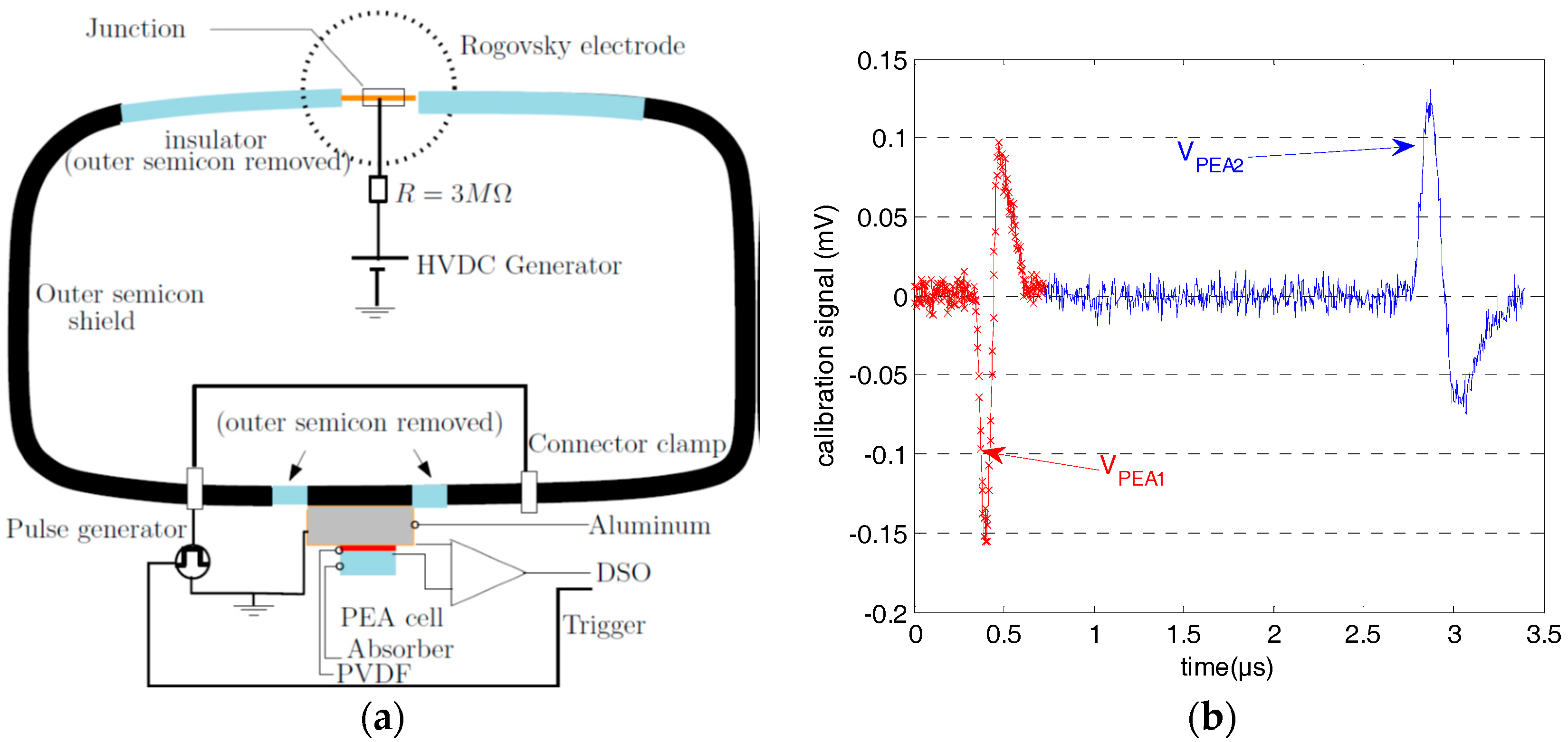
Historically, space charge measurement techniques have been implemented before the reconsideration of energy transport through HVDC. Several of these direct and non-destructive techniques, commonly known as "influence" or "stimuli" methods [5,6,7], have been developed. They do really represent essential tools for assessing materials in HVDC applications. They are based on the application of a mechanical, a thermal or an electrical stimulus which perturbs the electrostatic equilibrium in the test sample, giving birth to a transient response function of the charge distribution across the sample. While they have been applied for long on flat insulating samples of thickness typically larger than 100 µm, for various electrical engineering applications, there is still a very important matter, with the challenge of being able to determine the real field distribution in cable structures. In this respect, two techniques emerge, based either on a thermal perturbation, the thermal step method, or a field pulse perturbation, the Pulsed Electroacoustic (PEA) method. The space charge measurement on samples of full-size cables, with several cm thick insulation, has been demonstrated [8,9]. The challenges are now to adapt these techniques for type tests and online measurements under high voltage, on full-size cables [7,10,11,12].
We briefly describe here the PEA method in its version for cable geometry. The method uses a fast varying electric stress as the perturbation [13]. This voltage pulse produces a variation of the electrostatic force acting on each charge and thus creates elastic waves propagating from the charges and proportional to their density. These waves travel across the insulator at the speed of sound and can be detected by a piezoelectric transducer. The measured signal is an image of the charge distribution since elastic waves arrive at a time depending on the distance between the charges and the transducer. The spatial resolution of the method depends on the thickness of the sensor and the general bandwidth of the system, which is of the order of 100 MHz.
Features of the PEA method are the possibility of making acquisition with stress either on or off, its excellent time resolution, its relative lightness and the fact that it is widespread. A typical experimental arrangement for cable geometry is shown in Figure 1 [14]. It consists of a cable sample with a measurement device composed by a PEA cell including piezo sensor and amplifier, a DSO (Digital Signal Oscilloscope), a HVDC generator and a pulse generator (50 ns width, 10 kHz frequency and up to 5 kV amplitude). The voltage pulses are applied via the outer semiconductor shield (carbon-black-doped polymer, called semicon in the following) of the cable, whereas the high DC voltage is applied to the conductor of the cable. The outer semicon is set in intimate contact with the detection cell by applying a mechanical pressure on the cable. The acoustic response issued from many pulses is averaged in order to improve the signal-to-noise ratio: profiles were produced in 200 s time intervals.
Measurements are achieved in two steps: The calibration step consists in applying a small DC field to the sample and considering that the system response is that of the capacitive charges produced on the electrodes. From there the transfer function of the system can be isolated, accounting for the cylindrical geometry and attenuation and dispersion of acoustic waves in the material. Acoustic signals recorded in specific conditions are treated to provide charge distributions as detailed e.g., in [8,14].
The PEA method has been applied to produce the results shown in the next section for miniature cables. The version for flat specimen has been exploited to assess the performances of candidate materials for application to DC and was pushed to the characterization of multilayer dielectrics considering the Maxwell–Wagner effect and the field redistribution it implies [15]. We address in what follows the link between the direct information brought by this technique on the field distribution in cable geometry and the field distribution modeled based on the behavior of the electrical conductivity of the insulation.
2.2. Challenges Regarding Materials for HVDC Cables
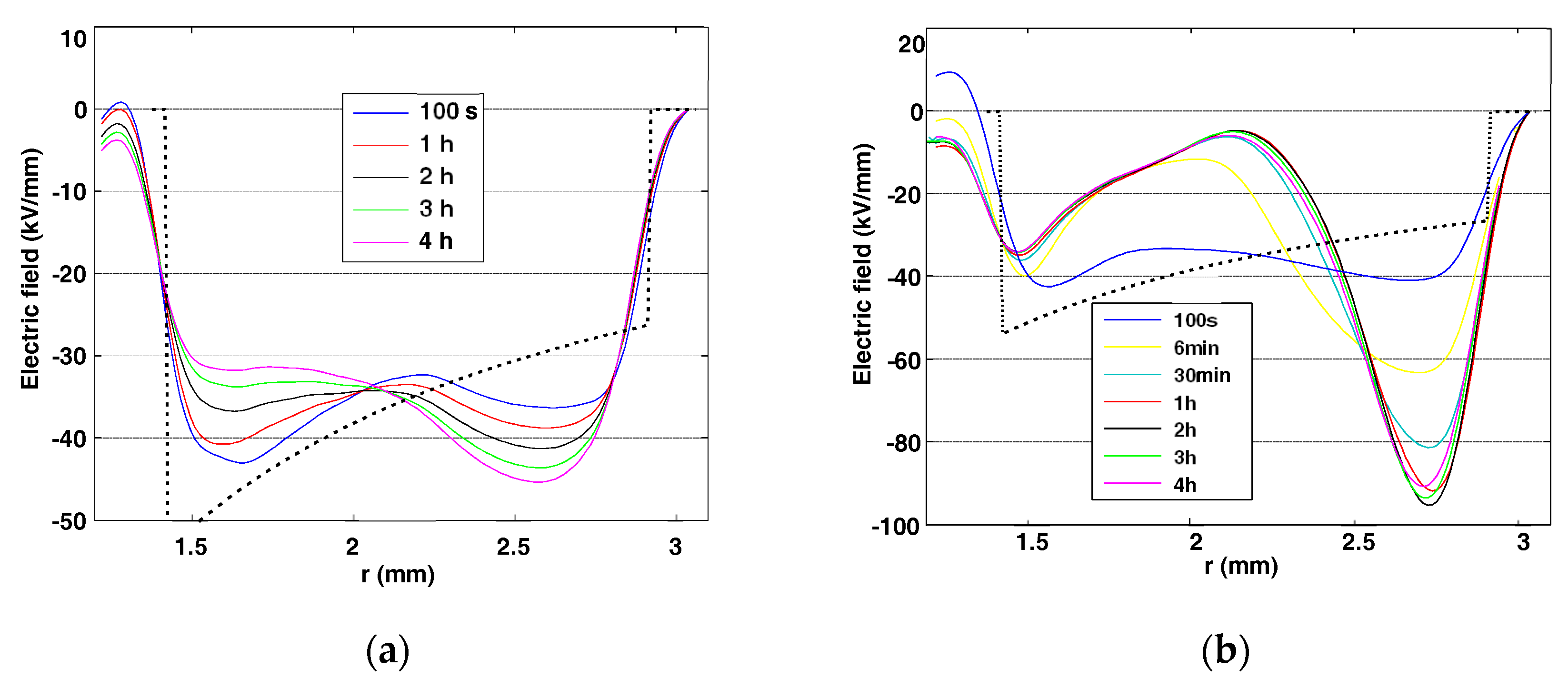
The crosslinking of polyethylene using peroxide initiator leads to the formation of by-products, i.e., chemicals as acetophenone, cumyl-alcohol or alpha-methyl-styrene. These by-products are known to favor the formation of space charges into the insulation, through processes not yet fully agreed: they can act as moieties capable of stabilizing charges, i.e., from an energy band diagram forming energy levels deep in the band gap [16], or forming ionized species that move into the insulation [8]. Figure 2 illustrates the consequences of the presence of such by-products considering field distribution obtained on miniature cables by PEA method. These cables, with 1.5 mm thick insulation, are representative structures of the full-size cables, with semiconducting screens at both inner and outer interfaces of the insulation. Results obtained on an extensively degassed cable and on a poorly degassed one are compared. The current in the cable loop was adjusted to set a temperature of 70 °C at the inner radius of the insulation and 60 °C at the outer radius. Measurements were realized with a DC voltage of −55 kV applied to the conductor with 4 h charging time and 4 h discharging time. Space charge profiles were acquired in 2 min interval times.
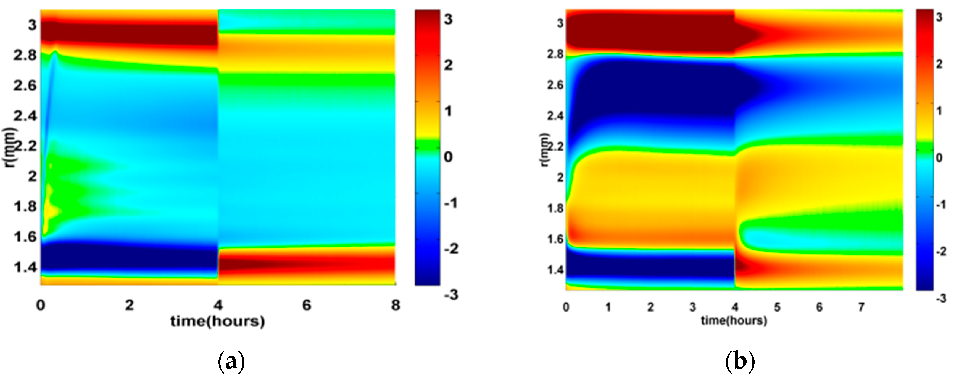
For the degassed cable, the field distribution moves as a function of charging time from a nearly capacitive shape (i.e., field larger near the inner semicon interface than near the outer) to a situation where the field is higher to the outer semicon. The maximum field remains in the range 40 to 45 kV/mm. Space charge patterns of Figure 3a reveal the progressive build-up of a negative space charge occupying the bulk of insulation. Two other features are noticeable: the formation of a positive homocharge adjacent to the anode, presumably due to hole injection, and the formation of a front of negative charges crossing the insulation in about 20 min. The latter has been explained by negative differential mobility for injected electrons [17].
In the case of the poorly degassed cable, the field is much higher as it reaches 100 kV/mm near the outer semicon, see Figure 2b. The features that are observed are clearly linked to the presence of by-products. The space charge density patterns plotted in Figure 3b reveal that a huge amount of negative charges is accumulated adjacent to the outer screen, whereas a positive space charge is formed close to the conductor. Such patterns correspond to heterocharge build-up, with as consequence the strengthening of the field next to the electrode. Note that at short time in Figure 3a, heterocharges seem to be quickly formed. This feature explains the deep in the field profile observed in Figure 2a.
The outgassing process (typically heating to 60 °C for several days) applied on these model cables cannot be up-scaled to full-size cables for the energetic cost. Present researches are oriented to the compounding of cables with reducing the amount of by-products. At the same time, the beneficial aspects of crosslinking on thermomechanical properties of cables must be maintained. We can mention here at least three strategies.
First, there is the development of crosslinking processes that substantially reduce the amount of by-products. This is the incremental strategy in new generation of raw materials commercialized for HVDC cables [18], with still using peroxide crosslinking. A more innovating route is that based on the use of co-agents of crosslinking with allylic functions, in which there is virtually no by-products [19]. Very promising results in terms of space charge features were obtained through such process, with a behavior approaching that obtained on un-crosslinked material, i.e., low density polyethylene [20].
The second strategy consists in using nanocomposite polymers [21,22] with the advantage of keeping on thermoplastics, i.e., avoiding the crosslinking process. It has been shown in several instances that with the incorporation of nanoparticles, the space charge accumulation in polymers is substantially reduced [23]. As examples, nanometer-size fillers of silica (SiO2) [24] and magnesium oxide (MgO) [25] incorporated into low-density polyethylene (LDPE) have been shown to be effective in suppressing space charge. The mechanisms behind those improvements are not completely clear at present [26], neither is the fate of the material integrity in time.
Finally there are some attempts of using Polypropylene insulation for its outstanding dielectric properties for being used as capacitors and its higher thermomechanical withstanding than polyethylene. New generation of mass impregnated cables have been recently proposed with Polypropylene Laminated Paper (PPLP) [27] as a laminated paper consisting of Polypropylene (PP) film and conventional Kraft paper.
2.3. Conductivity Models
Two approaches for the description of conduction in insulations can be mentioned with profound differences in the level of refinement of physical processes. Macroscopic models of conduction treat empirically or semi-empirically the conductivity through its dependence with the field and temperature. A well-known model formally applied to cables with oil-impregnated paper insulation is that of Eoll [28], who considered exponential functions for both the temperature and the field dependencies of the conductivity, without real physical justification.
As far as polymers are concerned, the variation in temperature finds more justification and experimental support with an Arrhenius law implying thermal activation of the charge transport. In the case of synthetic insulations, expressions of the form as given in Equation 2 were adopted in the literature for conductivity of synthetic cable insulators [29,30,31]:
Here Ea is the activation energy for conduction at low field, kB = 8.62 × 10⁻⁵ eV/K is the Boltzmann’s constant and other quantities are parameters. The second term with hyperbolic sine function finds physical justification in hopping conduction process as well as ionic conduction for example [32]. The equations used in this kind of approach can fit experimental data. The difficulty, however, is that they do not account for the effect of the nature of electrodes on conductivity, for example, or for the transient processes of conduction (charging currents), and more generally they do not reflect what is called space charge limited conduction. An alternative to macroscopic modelling is to follow the approaches used in semiconductor physics, with bringing details into the charge generation mechanisms, the electronic properties of materials at the interface, etc. These approaches have been developed in the last decades associating the physical concepts issued from semiconductor physics [33,34] and the numerical techniques capable of solving the problems, issued notably from gas physics [35]: The processes of charge injection, charge trapping, detrapping, mobility, etc. are incorporated in the model, with their accompanying set of parameters. One of the main difficulties here is to identify values of model parameters: they are many and cannot be extracted in a straightforward way by independent experiments. The conductivity does not appear explicitly, instead, it is the space- and time-dependent carrier density, the mobility and the local field that describe the transport. Such models have been set up mostly for flat specimen, but extension and resolution in cable geometry is appearing [36]. Also, it was used as a route to model breakdown under DC stress [37]. Although this is a promising route to develop accurate modelling of insulations, at present the full parameterization is still demanding; also the treatment of physical processes like ionization and heterocharge build-up is still in the infancy stage [38]. Owing to their complexity and to the strong dependence on the nature of polymers, such models cannot be easily handled as engineering tools aiming at dimensioning devices. One of the purposes of the present paper is to show how far the macroscopic models can account for the experimental behavior and also to touch the degree of approximation such macroscopic models bring in respect to physical mechanisms at play in insulating polymers.
3. Design-Related Space Charge in Model Cables
When dealing with space charge in mass-impregnated paper insulated cables, Morshuis and Jeroense [39] distinguished microscopic space charges as due to charges trapped at imperfections in the insulation from macroscopic space charge resulting from temperature and field dependency of the conductivity of the dielectric. Microscopic space charge cannot be anticipated easily as due most often to uncontrolled features. Macroscopic space charge can normally be anticipated if the conditions of the cable are known and materials are well characterized from the conductivity standpoint. Along this line, McAllister et al. [40] considered the accumulation of charge as the consequence of a non-uniform electrical conductivity. Within this family of, in principle, predictable space charge processes, one can also include the charge building-up at the interface between dielectrics of different nature (Maxwell–Wagner effect), and therefore the term macroscopic can be thought of as inappropriate [15,41]. In what follows, we will call it design-related space charges as this is essentially dependent on the arrangement of the system and applied stresses. We will focus on the fate of such charges at polarity inversion.
3.1. Constitutive Equations for the Space Charge
It is well known that the capacitive field distribution within the radius of a cable under AC voltage follows a distribution of the form:
where ri and ro are the inner and outer radii of the insulation in the cable.
In the case of DC stress, following Maxwell’s equation, here total current conservation, the electric field distribution in the cable insulation, in cylindrical geometry and under steady-state condition is given by [2,42]:
where Ec and σc are the electric field and the conductivity at the reference position rc. Equations (3) and (4) are equivalent only if σ is homogeneous, i.e., independent of r.
The conductivity gradient in a cable results from two processes. First, the field is non-homogeneous by geometry: a non-linear conductivity in field leads to a conductivity gradient. The second and main contribution is the Joule effect due to the current circulating in the conductor. This leads to a thermal gradient across the insulation of the form:
where Wc is the heat power dissipated per unit length of the conductor and λ is the thermal conductivity of the insulation in W/(m K).
The redistribution of the field goes with the formation of a space charge, whose density can be deduced based on the Poisson’s equation. This geometrical space charge density is of the form:
where ε is the dielectric permittivity of the material.
Considering Equation (6), and supposing a negative voltage applied to the conductor of the cable, it follows that the field is negative (resulting from ). As the last term is naturally negative (the high temperature and high electrical conductivity are to the conductor side), the expected space charge is negative. It is actually such a feature that is measured under thermal gradient in Figure 3a in the case of degassed cable.
If the conductivity depends only on the temperature according to an Arrhenius law with activation energy Ea, the charge density can be written as:
3.2. Test Conditions for Conductivity Measurements
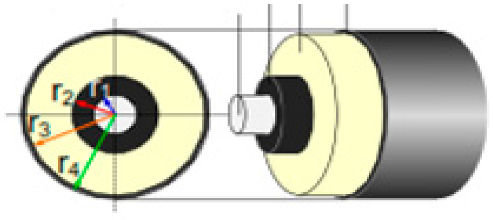
Experiments were performed on miniature cables consisting of an inner conductor, an inner semicon layer, the XLPE insulation of 1.5 mm in thickness and an outer semicon layer as depicted in Figure 4. This scaled-down test model of a DC power cable is produced by extrusion, the crosslinking process of the three-layer structure producing chemical bonds in the bulk of the insulation and of the semicon layers and at the semicon-insulation interfaces. The result is a chemical interface between the insulation and the semicon in the mini-cable which is similar to those found in a full-scale DC power cable. With this reduced dimension, the cost of production, transportation and testing of these cables is substantially reduced. Prior to measurements, the cables were thermally treated to remove crosslinking by-products.
Figure 5 shows a schematic of the setup for the conduction current measurements in the cable. The sample was peeled off by removing the outer semicon layer for preventing surface conduction. The guard sections are prepared with 20 mm length at both ends of the measurement area and 20 mm apart from the measurement section of 250 mm in length. The 1 m long specimen was installed as a ring inside the oven where both the end parts of the cable are jointed and connected to the 35 kV DC high-voltage generator from FuG Elektronik GmbH. The measurement and guard sections are connected to a Keithley 617 electrometer through a protecting circuit.
The measurements were performed under different temperatures varying from 30 °C to 90 °C by step of 10 °C. For each of the temperature levels, charging/discharging current measurements were realized for 11 values of applied voltage ranging between 2 and 30 kV under isothermal conditions with polarization/depolarization steps lasting for 1 h each. Note here that 1 h charging time can be judged as too short for estimating the conductivity. Interestingly, the charging currents were relatively stable after about 500 s (i.e., variation by less than a factor 0.5 between 500 s and 1 h) except for the lowest temperature and lowest field values when viewed in a log–log plot. Figure 6 shows an example of such transient charging currents obtained at a temperature of 50 °C. For the highest voltages, the current even tends to increase in time. So, we considered the current values obtained after 1 h as quasi-steady-state currents.
3.3. Results for Conductivity
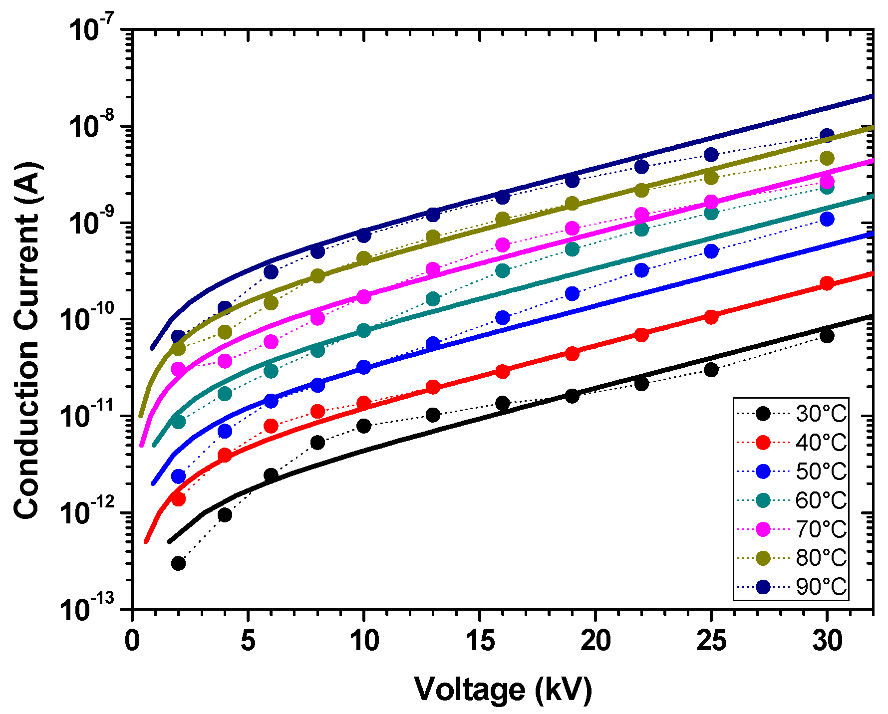
Figure 7 shows the results of conduction current measurements as a function of the field at different values of the temperature. The presented data correspond to charging currents obtained for 1 h of polarization time. We can see that the conduction currents are strongly dependent on field and temperature as the magnitudes are rising following the increase of temperature and field. The current values range from 0.3 pA at the lowest field and temperature (2 kV/30 °C) to 8 nA at the highest field and temperature (30 kV/90 °C).
Because of the cylindrical geometry of the samples and of the inhomogeneity of the field, it is necessary to take a hypothesis on the mathematical form of the expression of conductivity, σ, vs. field to convert I (V) curves into σ (E). We have supposed that the conductivity is of the form below, as successively used for flat XLPE specimen [15,29]:
Writing:
the current flowing in the outer circuit during the steady-state period at a given temperature can be written as:
where l is the length of the active part of the cable in current measurement. From Equation (10) one obtains the expression to determine the electric field at the radius r as follows:
In order to determine the parameters of the conductivity in Equation (8), we first estimated B and C values for measurements at a single temperature, considering the experimental quasi-steady-state charging currents. However, the relationship between current and field cannot be applied directly as would be the case in a flat geometry since the field distribution depends on the expected conductivity expression. To solve the problem, the electric field E(r) in Equation (11) is integrated from the inner to the outer radius: it gives the relationship between the applied voltage (Vapp) and the conduction current (quasi-steady-state current) as follows [43]:
where
In a first step, the fit of Vapp(I) to Equation (12) was achieved by non-linear curve fitting independently for each temperature level, so providing C(T) and B(T). We then deduced the activation energy Ea by linear regression to B × C vs. T−1 plot (Arrhenius plot) considering that at sufficiently low field the conductivity is approximated by: σ(T) = B(T) × C(T). Finally, as C did not appear significantly temperature-dependent, we considered a constant value. The following final quantities were obtained for conductivity equation: C = 2.15 × 10⁻⁷ m/V, A = 3.83 × 10⁴ S.V/m² and Ea = 0.83 eV.
Figure 7 shows the fit obtained to experimental current values and Figure 8 illustrates the conductivity vs. E and T obtained by the voltage–current model. We can appreciate that a threshold-like behaviour comes out from the representation, with a threshold field independent of temperature, which is Et ≈ 12 kV/mm. The relation to the value of C, which actually controls the threshold, can be deduced as Et ≈ 2.5 /C. Below the threshold, the response tends to follow Ohm’s law, which means that the conductivity is independent from field, but as the field is increasing, it begins to be a non-linear relation. The reason can be space charge effects that accumulate at high fields through, for example, space charge limited current. An alternative would be to have a hopping conduction with charge mobility dependent on the field. The two processes may have different temperature dependencies for the threshold. With the assumption of using a constant C value in the fitting process, supported by the data, we cannot reveal this feature in the modelled temperature-dependent conductivity characteristic.
3.4. Electric Field Simulation Based on Conductivity Data
We have followed the route consisting in using the conductivity model as input to finite element modelling (FEM) of the field distribution in cables under thermal gradient. Such approach was previously applied on Medium Voltage cables to estimate space charge and field profiles as a function of time [42] and also to deduce the shape of the transient current in the case of miniature cables [43]. The numerical resolution by FEM was achieved using Comsol software. At the initial stage, one considers a purely capacitive field distribution, cf. Equation (3), hypothesizing a charge-free system. The temperature distribution was modelled according to Equation (5), supposing the system in thermal equilibrium. The numerical resolution was achieved in 1D in time supposing the conductivity obeys to Equation (8).
The first simulation set was run at an applied voltage of 15 kV, with a polarization time of 2 h and considering that 10 °C of thermal gradient is applied across the insulation at the mean temperature of 65 °C. The conductor temperature is 70 °C and the outer temperature of the insulation is 60 °C. The field profiles of Figure 9 show decreasing trends in time near the conductor and increasing at the outer part of insulation. At the first 100 s, the maximum field is at the inner semicon-insulation interface, being 13.5 kV/mm, while the minimum field is at the insulation-outer semicon interface and is 7.4 kV/mm. As the time passes, there is field redistribution in the insulation due to the gradient in conductivity induced by the thermal gradient.
The field near the conductor tends to decrease following the polarization time, whereas the field at the outer interface of insulation-semicon increases. After 2 h of polarization, the field inversion is shown where the field near the conductor has dropped to 9.8 kV/mm, which is lower than that at the outer insulation where the magnitude reached is over 10 kV/mm. This phenomenon of stress inversion is not very strong here as the conductivity is non-linear in field according to the results: in a way, it counterbalances the temperature effect on conductivity.
We consider next the case of polarity reversal simulation in isothermal condition at temperature of 65 °C, hypothesizing that there is no load operating in the cable. Figure 10 shows the simulation results of electric field profiles with inverting the voltage from +15 to −15 kV after 2 h charging time. The field profile across the insulation thickness clearly changes along 2 h polarization time. The effect is only due to the non-linear conductivity with field, which tends to homogenize the field in the insulation, acting as field grading. This profile is similar to the Laplacian-field profile (considered at t = 0 s). The time constant for charge build-up is considering average field and temperature of 10 kV/mm and 65 °C (σ = 7.0 × 10⁻¹⁵ S/m). Therefore, in a 2 h charging time the steady state is reached.
Comparing to the positive polarity steps, the field profile at the inversion step is slightly higher. This is due to the residual field built up under the positive step. We can see in Figure 10 that the field magnitude at the inner semicon at −15 kV after 300 s of voltage inversion, that is 15.1 kV/mm is higher than the one at the same instant in the positive step, which is 13.4 kV/mm. The profile indexed as “0 V” represents the residual field estimated after the inversion. It amounts to about 15% of the Laplacian field.
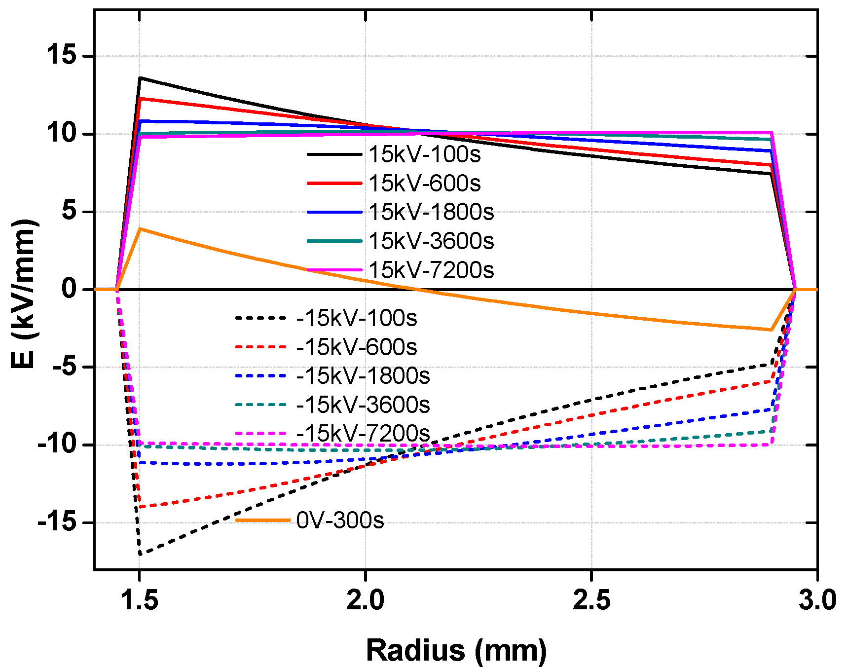
Figure 11 shows the simulation results of electric field profile at +15 kV to −15 kV voltage polarity inversion applied with 10 °C thermal gradient and 2 h polarization time. The mean temperature is set to 65 °C. The voltage polarity inversion does make the field profile at the negative step higher than at the positive step, at the inner semicon-insulation interface. Its magnitude difference is equal to the residual field after the polarization step.
When thermal gradient is applied across the insulation, while current homogenization in the insulation takes place and space charges settle, the field profile at the inner semicon decreases and it increases at the outer semicon. This phenomenon of field inversion is the same as the one occurred in the first simulation, but with the influence of voltage polarity inversion, the variation of field is substantially higher than in isotherm condition. The field at the inner semicon is decreased from 17 kV/mm to 9.9 kV/mm, and at the outer semicon is increased from 4.7 kV/mm to 9.9 kV/mm.
3.5. Discussion
Voltage polarity inversion is the way the flow of energy can be reversed when using conventional line-commutated converters (LCC). More and more, voltage source converters (VSC) tend to be preferred over LCC owing to their ability to independently control the reactive power flow, the faster dynamic response and the possibility to connect to weak AC networks [44,45]. These are typical situations in networks with substantial introduction of renewable energy [46]. LCC tend to be dedicated to high-power HVDC links with stable networks. At the transmission level, the advantage of VSC is the absence of polarity inversion for inverting the energy flux. This feature has of course given credit to HVDC cables with synthetic insulation. Indeed, polymeric insulations tend to accumulate electrical charges and therefore make materials and cables more sensitive to voltage inversion and to voltage variations in a general way.
There are anyway at least two reasons to address the cable behavior under polarity inversion. The first one is the case of incident on the transmission line: Pole-to-ground faults on the DC link or faults inside neighboring AC grids may have an impact on the VSC-HVDC system [47], with transients constituted of over-voltages and voltage inversion. The second one is the case of maintenance and replacement of already existing lines with LCC systems installed. An example of it is the refurbishment of part of the underground IFA2000 cable link of +/−270 kV between France and UK made of mass-impregnated paper to be replaced by a XLPE insulated cable.
The above results on miniature cables have shown that in the polarity inversion stage, the electric field at the inner semicon is strongly enhanced, by about 30% in respect to the capacitive field and 70% of the steady-state field previously settled. The chosen stresses, being average temperature of 65 °C and geometrical field at the inner conductor of 15 kV/mm, are realistic and by no means overestimated in respect to possible service conditions. It also shows that the characteristic time for charge redistribution is relatively long, of several tens of minutes. This means that the field excess can be exerted for a significant part of the life of the cable. In accessories such as joints and terminations, that exhibit more complex geometries and involve the association of dielectrics of different nature, a similar approach is to be developed, in non-stationary conditions, in order to identify hot points in field and anticipate their occurrence in time and space [48].
Besides, the computations consider only the design-related space charge, i.e., that induced by the conductivity gradient. The measurements of space charge and field distributions, in general, reveal other features than this conductivity-related contribution, linked to the charge trapping and to the internal dissociation of charges. Charge trapping, specifically, may produce longer discharge time than expected. Because of these extra contributions to space charges, the measured field distortions tend to be higher than predicted [42]. Though the trend with a decrease in time of the field at the inner semicon and an increase at the outer semicon observed experimentally in Figure 2a are confirmed by the model, extra field inhomogeneity is present at short time that is presumably due to charge trapping and heterocharge formation. Therefore, the computation of the conductivity and field alone cannot ensure that the field remains in the expected limits and space charge and field distribution measurements are recommended to assess the material behavior. More sophisticated fluid models should be developed in order to account for the complete behavior [36]. It goes with space charge acquisition on model cables at different temperatures, which remains still seldom in the literature.
4. Conclusions
The field distribution within the insulation of cables under thermal gradient and polarity inversion can be obtained through simulation based on electrical conductivity data for the insulating material as a function of field and temperature. The electrical conductivity of the insulating material can be obtained based on current measurements on samples in cable geometry. However, because of the divergence of the field, a hypothesis has to be taken about the form of the field dependence of the conductivity. We have provided a method to obtain the coefficients defining conductivity as a function of temperature and field. The dependency of the conductivity on field makes the insulation act as a field grading material: in isothermal conditions, the field in model cables is homogenized in respect to the capacitive field distribution with notably a reduction of 10% of the maximum field.
The conductivity gradient under thermal gradient applied combined to the non-linearity in field leads to homogenization of the field in the insulation for voltage of 15 kV. The stress inversion phenomenon did not appear in the conditions of simulation. At short time, there is field strengthening just after polarity inversion, representing possible aging route for the present case. The approach is to be generalized considering typical mission profiles for the system, identifying thermal stresses and induced electrical stresses in non-stationary conditions, and treating the case of accessories that remain critical parts of cable systems.
Direct measurement of space charge on properly outgassed cables show that some trends can be anticipated by modelling. For example, the reduction of the field at the inner semicon and its increase at the outer semicon are reproduced. However, the shape of the field distribution is not fully in agreement with that expected from the conductivity model. The deviations that are observed are probably not the consequence of an erroneous choice of the conductivity law. Rather, it results from charge trapping into the insulation.
To account for these processes, more rigorous models incorporating charge injection, trapping, detrapping, recombination should be developed. This is, however, a difficult task considering the complexity of XLPE, its evolution with the compounding and the heavy procedure for parameterizing the physical processes. The case of heterocharge formation, presumably due to field-induced ionization, is still to be modeled as only scarce reports treat this process. The evidence of these effects is illustrated by the heavy field distortion revealed in space charge measurements with poor cable outgassing.
The access to field distribution by experimental techniques leads in conclusion to question about the field distribution that can be anticipated by macroscopic models of conduction.
Acknowledgments
We acknowledge PLN for the financial support during the research stay of Nugroho Adi in Laplace Laboratory, University Paul Sabatier, Toulouse III, France.
Author Contributions
Nugroho Adi worked the conductivity set-up, carried out the measurements and parameterized the model. Thi Thu Nga Vu realized space charge measurements and FEM modelling. Fulbert Baudoin developed fitting approach to conductivity in cables. Gilbert Teyssèdre and Ngapuli Sinisuka wrote the paper.
Conflicts of Interest
The authors declare no conflict of interest.
Abbreviations
The following abbreviations are used in this manuscript:
| DSO | Digital Signal Oscilloscope |
| HVAC | High-Voltage Alternate Current |
| HVDC | High-Voltage Direct Current |
| LCC | Line Commutated Converter |
| LDPE | Low Density Polyethylene |
| PEA | Pulsed Electroacoustic |
| PPLP | Polypropylene Laminated Paper |
| VSC | Voltage Source Converter |
| XLPE | Crosslinked Polyethylene |
References
- Mazzanti, G.; Marzinotto, M. Extruded Cables for High-Voltage Direct-Current Transmission; Wiley-IEEE Press: Hoboken, NJ, USA, 2013. [Google Scholar]
- Fabiani, D.; Montanari, G.C.; Laurent, C.; Teyssedre, G.; Morshuis, P.H.F.; Bodega, R.; Dissado, L.A. HVDC cable design and space charge accumulation. Part 3: Effect of temperature gradient. IEEE Electr. Insul. Mag. 2008, 24, 5–14. [Google Scholar] [CrossRef]
- Montanari, G.C. The electrical degradation threshold of polyethylene investigated by space charge and conduction current measurements. IEEE Trans. Dielectr. Electr. Insul. 2000, 7, 309–315. [Google Scholar] [CrossRef]
- Dissado, L.A.; Laurent, C.; Montanari, G.C.; Morshuis, P.H.F. Demonstrating a threshold for trapped space charge accumulation in solid dielectrics under DC field. IEEE Trans. Dielectr. Electr. Insul. 2005, 12, 612–620. [Google Scholar] [CrossRef]
- Holé, S.; Ditchi, T.; Lewiner, J. Non-destructive methods for space charge distribution measurements: What are the differences? IEEE Trans. Dielectr. Electr. Insul. 2003, 10, 670–677. [Google Scholar] [CrossRef]
- Fukunaga, K. Progress and prospects in PEA space charge measurement techniques. IEEE Electr. Insul. Mag. 2008, 24, 26–37. [Google Scholar] [CrossRef]
- Notingher, P.; Holé, S.; Berquez, L.; Teyssedre, G. An insight into space charge measurements. Int. J. Plasma Environ. Sci. Technol. 2017, 11, 26–37. [Google Scholar]
- Hozumi, N.; Takeda, T.; Suzuki, H.; Okamoto, T. Space charge behavior in XLPE cable insulation under 0.2–1.2 MV/cm dc fields. IEEE Trans. Dielectr. Electr. Insul. 1998, 5, 82–90. [Google Scholar] [CrossRef]
- Castellon, J.; Notingher, P.; Agnel, S.; Toureille, A.; Matallana, J.; Janah, H.; Mirebeau, P.; Sy, D. Industrial installation for voltage-on space charge measurements in HVDC cable. In Proceedings of the Industry Applications Conference, Hong Kong, China, 2–6 October 2005; pp. 1112–1118. [Google Scholar]
- Hozumi, N.; Hori, M. Measuring space-charge in HVDC cables. Energize 2017, 2, 35–38. [Google Scholar]
- Mazzanti, G.; Chen, G.; Fothergill, J.C.; Hozumi, N.; Li, J.; Marzinotto, M.; Mauseth, F.; Morshuis, P.; Reed, C.; Tzimas, A.; et al. A protocol for space charge measurements in full-size HVDC extruded cables. IEEE Trans. Dielectr. Electr. Insul. 2015, 22, 21–34. [Google Scholar] [CrossRef]
- Tzimas, A.; Boyer, L.; Mirebeau, P.; Dodd, S.; Castellon, J.; Notingher, P. Qualitative analysis of PEA and TSM techniques on a 200kV extruded cable during a VSC ageing program. In Proceedings of the IEEE International Conference on Dielectrics (ICD), Montpellier, France, 3–7 July 2016; pp. 49–52. [Google Scholar]
- Maeno, T.; Kushiba, H.; Takada, T.; Cooke, C.M. Pulsed electro-acoustic method for the measurement of volume charge in e-beam irradiated PMMA. In Proceedings of the IEEE Electrical Insulation & Dielectric Phenomena, Amherst, NY, USA, 20–24 October 1985; pp. 389–397. [Google Scholar]
- Vissouvanadin, B.; Vu, T.T.N.; Berquez, L.; Le Roy, S.; Teyssèdre, G.; Laurent, C. Deconvolution techniques for space charge recovery using pulsed electroacoustic method in coaxial geometry. IEEE Trans. Dielectr. Electr. Insul. 2014, 21, 821–828. [Google Scholar] [CrossRef]
- Vu, T.T.N.; Teyssedre, G.; Vissouvanadin, B.; Le Roy, S.; Laurent, C. Correlating conductivity and space charge measurements in multi-dielectrics under various electrical and thermal stresses. IEEE Trans. Dielectr. Electr. Insul. 2015, 22, 117–127. [Google Scholar] [CrossRef]
- Meunier, M.; Quirke, N.; Aslanides, A. Molecular modeling of electron traps in polymer insulators: Chemical defects and impurities. J. Chem. Phys. 2001, 115, 2876–2881. [Google Scholar] [CrossRef]
- Teyssedre, G.; Vu, T.T.N.; Laurent, C. Negative differential mobility for negative carriers as revealed by space charge measurements on crosslinked polyethylene insulated model cables. Appl. Phys. Lett. 2015, 107, 252901. [Google Scholar] [CrossRef]
- Hjertberg, T.; Englund, V.; Hagstrand, P.O.; Loyens, W.; Nilsson, U.; Smedberg, A. Materials for HVDC cables. Revue Electricite Electronique 2014, 4, XI–XV. [Google Scholar]
- Gard, J.C.; Denizet, I.; Mammeri, M. Development of a XLPE insulating with low peroxide by-products. In Proceedings of the 9th International Conference on Insulated Power Cables, Versailles, France, 21–25 June 2015; pp. 1–5. [Google Scholar]
- Vu, T.T.N.; Teyssedre, G.; Le Roy, S.; Laurent, C. Space charge criteria in the assessment of insulation materials for HVDC. IEEE Trans. Dielectr. Electr. Insul. 2017, 24, 1405–1415. [Google Scholar] [CrossRef]
- Tanaka, T.; Kindersberger, J.; Frechette, M.; Gubanski, S.; Vaughan, A.S.; Sutton, S.; Morshuis, P.; Mattmann, J.P.; Montanari, G.C.; Reed, C.; et al. Polymer Nanocomposites—Fundamentals and Possible Applications to Power Sector; CIGRE: Paris, France, 2011. [Google Scholar]
- Pourrahimi, A.M.; Hoang, T.A.; Liu, D.; Pallon, L.K.H.; Gubanski, S.; Olsson, R.T.; Gedde, U.W.; Hedenqvist, M.S. Highly efficient interfaces in nanocomposites based on polyethylene and ZnO nano/hierarchical particles: A novel approach toward ultralow electrical conductivity insulations. Adv. Mater. 2016, 28, 8651–8657. [Google Scholar] [CrossRef] [PubMed]
- Tanaka, T.; Imai, T. Advances in nanodielectric materials over the past 50 years. IEEE Electr. Insul. Mag. 2013, 29, 10–23. [Google Scholar] [CrossRef]
- Huang, X.Y.; Jiang, P.K.; Yin, Y. Nanoparticle surface modification induced space charge suppression in linear low density polyethylene. Appl. Phys. Lett. 2009, 95, 242905. [Google Scholar] [CrossRef]
- Murakami, Y.; Nemoto, M.; Okuzumi, S.; Masuda, S.; Nagao, M.; Hozumi, N.; Sekiguchi, Y.; Murata, Y. DC conduction and electrical breakdown of MgO/LDPE nanocomposite. IEEE Trans. Dielectr. Electr. Insul. 2008, 15, 33–39. [Google Scholar] [CrossRef]
- Nelson, J.K. Nanodielectrics—The first decade and beyond. In Proceedings of the Electrical Insulating Materials (ISEIM), Niigata, Japan, 1–5 June 2014; pp. 1–11. [Google Scholar]
- Chen, G.; Hao, M.; Xu, Z.Q.; Vaughan, A.; Cao, J.Z.; Wang, H.T. Review of high voltage direct current cables. CSEE J. Power Energy Systems 2015, 1, 9–21. [Google Scholar] [CrossRef]
- Eoll, C.K. Theory of stress distribution in insulation of High-Voltage DC cables: Part I. IEEE Trans. Electr. Insul. 1975, 10, 27–35. [Google Scholar] [CrossRef]
- Boggs, S.; Dwight, H.; Hjerrild, J.; Holbol, J.T.; Henriksen, M. Effect of insulation properties on the field grading of solid dielectric DC cable. IEEE Trans. Power Deliv. 2001, 16, 456–462. [Google Scholar] [CrossRef]
- Choo, W.; Chen, G.; Swingler, S.G. Electric field in polymeric cable due to space charge accumulation under DC and temperature gradient. IEEE Electr. Insul. Mag. 2011, 25, 596–606. [Google Scholar] [CrossRef]
- Qin, S.; Boggs, S. Design considerations for High Voltage DC components. IEEE Electr. Insul. Mag. 2012, 28, 36–44. [Google Scholar] [CrossRef]
- Teyssedre, G.; Laurent, C. Charge transport modeling in insulating polymers: From molecular to macroscopic scale. IEEE Trans. Dielectr. Electr. Insul. 2005, 12, 857–875. [Google Scholar] [CrossRef]
- Alison, J.M.; Hill, R.M. A model for bipolar charge transport, trapping and recombination in degassed crosslinked polyethene. J. Phys. D Appl. Phys. 1994, 27, 1291–1299. [Google Scholar] [CrossRef]
- Le Roy, S.; Teyssedre, G.; Laurent, C.; Montanari, G.C.; Palmieri, F. Description of charge transport in polyethylene using a fluid model with a constant mobility: fitting model and experiments. J. Phys. D Appl. Phys. 2006, 39, 1427–1436. [Google Scholar] [CrossRef]
- Le Roy, S.; Segur, P.; Laurent, C.; Teyssedre, G. Description of bipolar charge transport in polyethylene using a fluid model with a constant mobility: model prediction. J. Phys. D Appl. Phys. 2004, 37, 298–305. [Google Scholar] [CrossRef]
- Le Roy, S.; Teyssèdre, G.; Laurent, C. Modelling space charge in a cable geometry. IEEE Trans. Dielectr. Electr. Insul. 2016, 23, 2361–2367. [Google Scholar] [CrossRef]
- Li, S.; Zhu, Y.; Min, D.; Chen, G. Space charge modulated electrical breakdown. Sci. Rep. 2016, 6, 32588. [Google Scholar] [CrossRef] [PubMed]
- Le Roy, S.; Teyssedre, G. Ion generation and transport under electric stress in a low density polyethylene matrix. In Proceedings of the IEEE Annual Report Conference on Electrical Insulation and Dielectric Phenomena (CEIDP), Ann Arbor, MI, USA, 18–21 October 2015; pp. 63–66. [Google Scholar]
- Morshuis, P.; Jeroense, M. Space charge in HVDC cable insulation. In Proceedings of the IEEE Annual Report Conference on Electr. Insul. Dielectr. Phenom. (CEIDP), Minneapolis, MN, USA, 9–22 October 1997; pp. 28–31. [Google Scholar]
- McAllister, I.W.; Crichton, G.C.; Pedersen, A. Charge accumulation in DC cables: A macroscopic approach. In Proceedings of the IEEE International Symposium on Electrical Insulation, Pittsburgh, PA, USA, 5–8 June 1994; pp. 212–216. [Google Scholar]
- Delpino, S.; Fabiani, D.; Montanari, G.C.; Laurent, C.; Teyssedre, G.; Morshuis, P.H.F.; Bodega, R.; Dissado, L.A. Polymeric HVDC cable design and space charge accumulation. Part 2: Insulation interfaces. IEEE Electr. Insul. Mag. 2008, 24, 14–24. [Google Scholar] [CrossRef]
- Vu, T.T.N.; Teyssèdre, G.; Vissouvanadin, B.; Le Roy, S.; Laurent, C.; Mammeri, M.; Denizet, I. Field distribution in polymeric MV-HVDC model cable under temperature gradient : Simulation and space charge measurements. Eur. J. Electr. Engg. 2014, 17, 307–325. [Google Scholar]
- Vu, T.T.N.; Teyssedre, G.; Vissouvanadin, B.; Steven, J.Y.; Laurent, C. Transient space charge phenomena in HVDC model cables. In Proceedings of the 9th International Conference on Insulated Power Cables (JiCable), Versailles, France, 21–25 June 2015; pp. 1–6. [Google Scholar]
- Shao, S.J.; Agelidis, V.G. Review of DC system technologies for large scale integration of wind energy systems with electricity grids. Energies 2010, 3, 1303–1319. [Google Scholar] [CrossRef]
- Bresesti, P.; Kling, W.L.; Hendriks, R.L.; Vailati, R. HVDC connection of offshore wind farms to the transmission system. IEEE Trans. Energy Convers. 2007, 22, 37–43. [Google Scholar] [CrossRef]
- Brenna, M.; Foiadelli, F.; Longo, M.; Zaninelli, D. Improvement of wind energy production through HVDC systems. Energies 2017, 10, 157. [Google Scholar] [CrossRef]
- Jardini, J.A.; Vasquez-Arnez, R.L.; Bassini, M.T.; Horita, M.A.B.; Saiki, G.Y.; Cavalheiro, M.R. Overvoltage assessment of point-to-point VSC-based HVDC systems. Przegląd Elektrotechniczny 2015, 8, 105–122. [Google Scholar] [CrossRef]
- Vu, T.T.N.; Teyssedre, G.; Le Roy, S.; Laurent, C. Maxwell-Wagner effect in multi-layered dielectrics: Interfacial charge measurement and modelling. Technologies 2017, 5, 27. [Google Scholar] [CrossRef]
Figure 1.
(a) Schematic of the Pulsed Electroacoustic (PEA) test bench for cable geometry. PVDF—Poly(vinylidene fluoride) is the material for the piezoelectric sensor. The cable is arranged as a loop so that an AC current can be created in it using a current transformer to reach the desired thermal conditions (thermal gradient); (b) Rough signal measured for the calibration step by applying 20 kV on a 4.5 mm thick insulation Medium Voltage (MV) cable [14].

Figure 2.
Field distribution obtained in the insulation of miniature cable samples with 1.5 mm thick insulation. Measurements were achieved under a thermal gradient of 10 °C, (Tin = 70 °C; Tout = 60 °C), under a voltage of −55 kV applied to the conductor. (a) degassed sample; (b) partly degassed sample. The dashed curve is the geometric field distribution.

Figure 3.
Space charge density patterns corresponding to field profiles shown in Figure 1. The color scale represents charge density in C/m3. (a) degassed sample; (b) partly degassed sample.
Figure 3.
Space charge density patterns corresponding to field profiles shown in Figure 1. The color scale represents charge density in C/m3. (a) degassed sample; (b) partly degassed sample.

Figure 4.
Schematic representation of DC miniature cable used for testing: Conductor radius r1 = 0.65 mm; Inner semicon radius r2 = ri =1.45 mm; Insulation radius r3 = ro = 2.95 mm; Outer semicon radius r4 = 3.65 mm.
Figure 4.
Schematic representation of DC miniature cable used for testing: Conductor radius r1 = 0.65 mm; Inner semicon radius r2 = ri =1.45 mm; Insulation radius r3 = ro = 2.95 mm; Outer semicon radius r4 = 3.65 mm.

Figure 5.
Conduction current measurement setup.
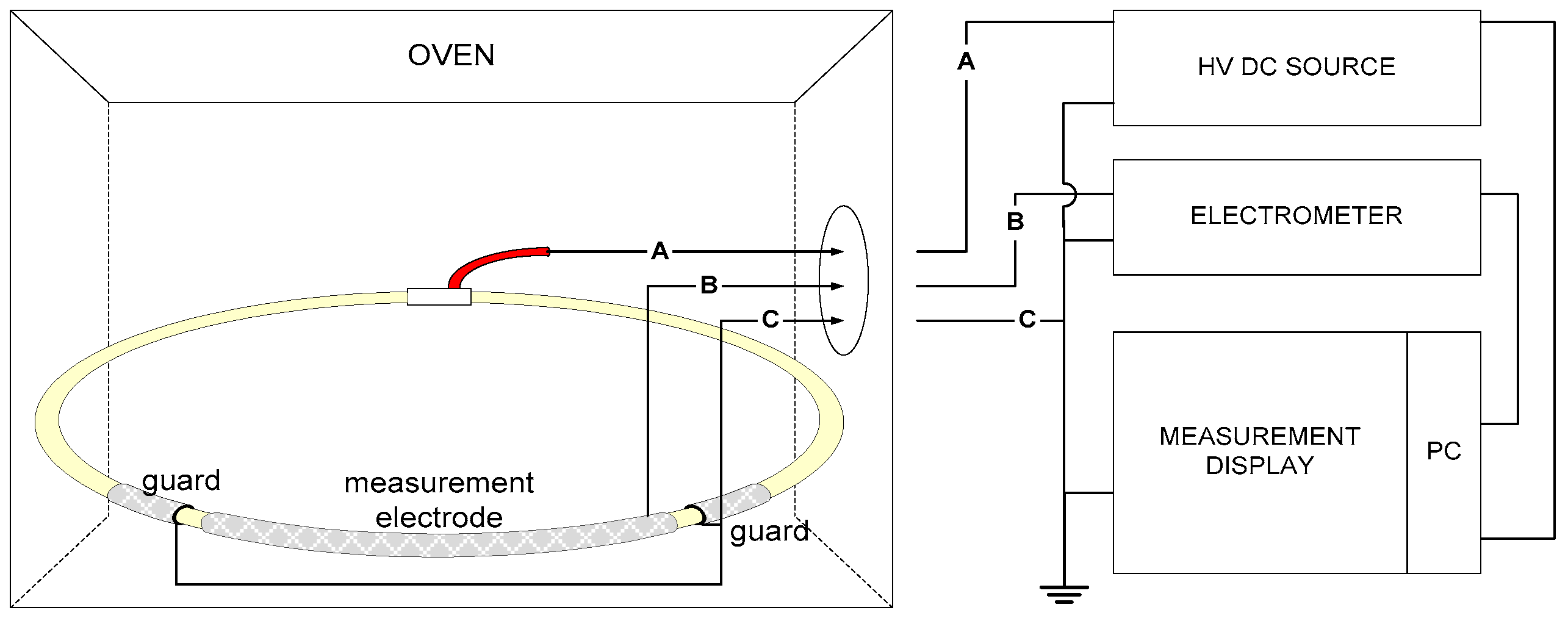
Figure 6.
Charging current transients under different fields at a temperature of 50 °C. Currents were measured in 2 s intervals all along the cycle.
Figure 6.
Charging current transients under different fields at a temperature of 50 °C. Currents were measured in 2 s intervals all along the cycle.
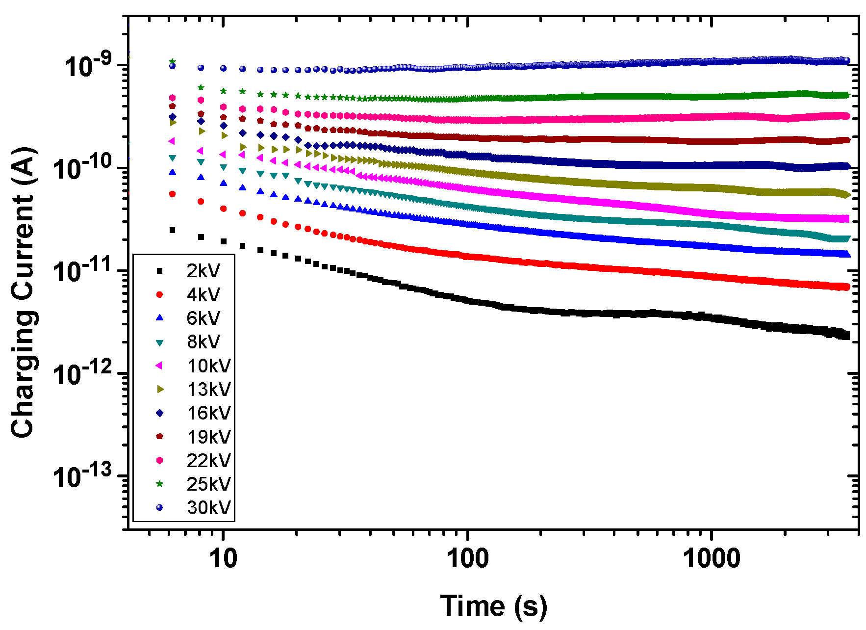
Figure 7.
Conduction current results as a function of field at various temperatures. The solid lines are the results from the fit functions to the conductivity equation.
Figure 7.
Conduction current results as a function of field at various temperatures. The solid lines are the results from the fit functions to the conductivity equation.

Figure 8.
Conductivity vs. field and temperature (in 10 °C step) obtained from the model.
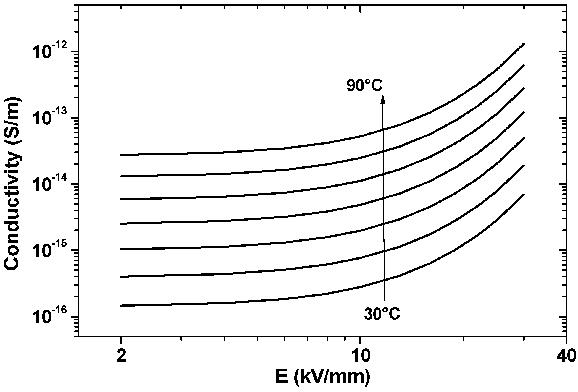
Figure 9.
Modeled field distribution profiles in a cable sample with a temperature gradient of 10 ˚C at an applied voltage of 15 kV.
Figure 9.
Modeled field distribution profiles in a cable sample with a temperature gradient of 10 ˚C at an applied voltage of 15 kV.
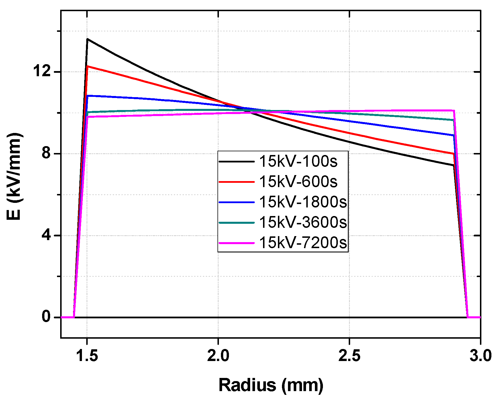
Figure 10.
Modeled field distribution profiles in a cable sample under voltage inversion applied and at isotherm condition at T = 65 °C.
Figure 10.
Modeled field distribution profiles in a cable sample under voltage inversion applied and at isotherm condition at T = 65 °C.
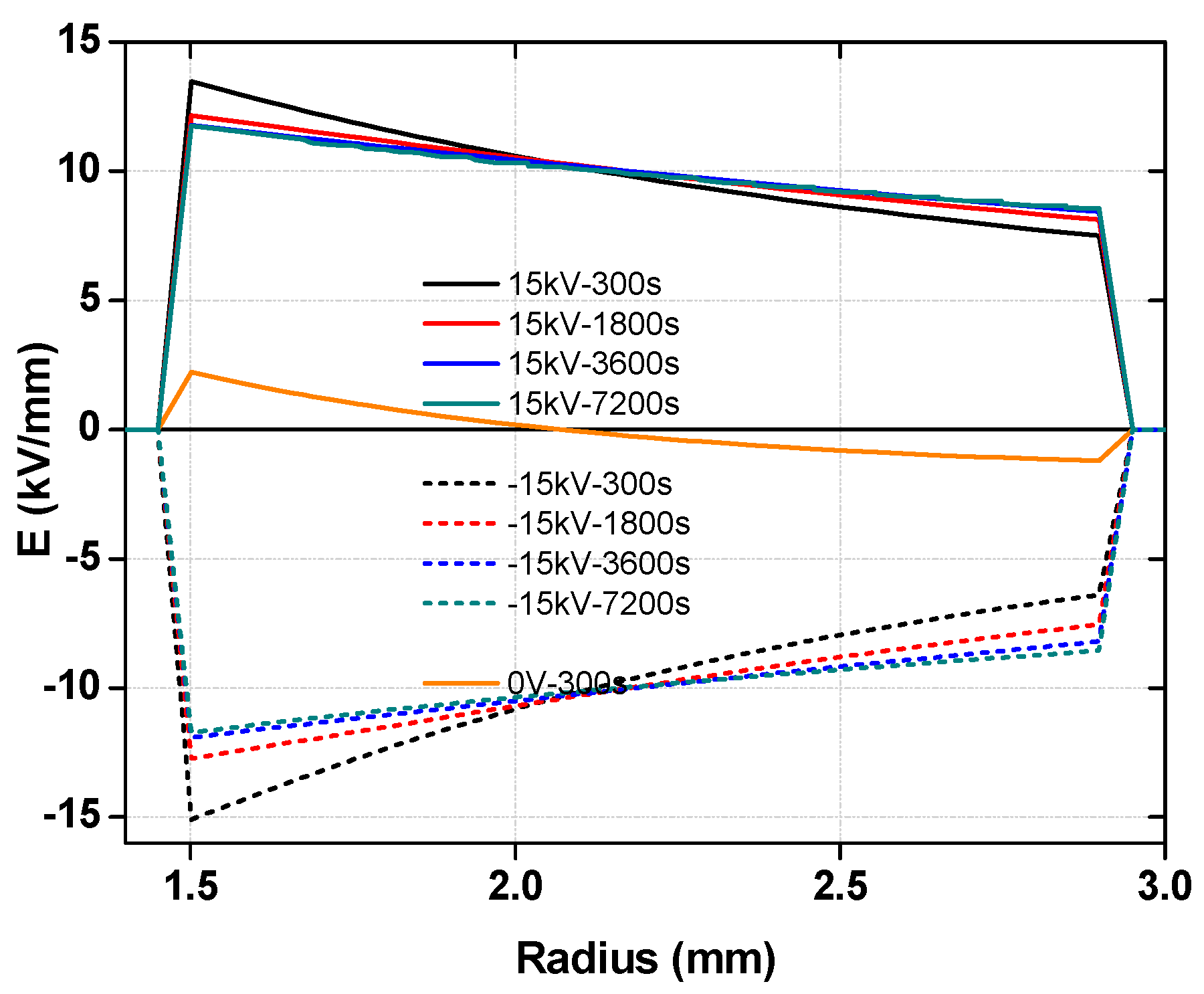
Figure 11.
Field distribution profiles in a cable sample with voltage inversion applied from +15 kV to −15 kV and at T gradient = 10 ˚C. The curve indexed 0 V-300 s is the field distribution after 300 s in the short-circuit applied after the negative voltage step.
Figure 11.
Field distribution profiles in a cable sample with voltage inversion applied from +15 kV to −15 kV and at T gradient = 10 ˚C. The curve indexed 0 V-300 s is the field distribution after 300 s in the short-circuit applied after the negative voltage step.

© 2017 by the authors. Licensee MDPI, Basel, Switzerland. This article is an open access article distributed under the terms and conditions of the Creative Commons Attribution (CC BY) license (http://creativecommons.org/licenses/by/4.0/).
Share and Cite
MDPI and ACS Style
Adi, N.; Vu, T.T.N.; Teyssèdre, G.; Baudoin, F.; Sinisuka, N. DC Model Cable under Polarity Inversion and Thermal Gradient: Build-Up of Design-Related Space Charge. Technologies 2017, 5, 46. https://doi.org/10.3390/technologies5030046
AMA Style
Adi N, Vu TTN, Teyssèdre G, Baudoin F, Sinisuka N. DC Model Cable under Polarity Inversion and Thermal Gradient: Build-Up of Design-Related Space Charge. Technologies. 2017; 5(3):46. https://doi.org/10.3390/technologies5030046
Chicago/Turabian StyleAdi, Nugroho, Thi Thu Nga Vu, Gilbert Teyssèdre, Fulbert Baudoin, and Ngapuli Sinisuka. 2017. "DC Model Cable under Polarity Inversion and Thermal Gradient: Build-Up of Design-Related Space Charge" Technologies 5, no. 3: 46. https://doi.org/10.3390/technologies5030046
Note that from the first issue of 2016, this journal uses article numbers instead of page numbers. See further details here.