In-Situ Contact Surface Characterization in a MEMS Ohmic Switch under Low Current Switching


Mechanical Engineering, University of Southampton, Southampton SO17 1BJ, UK
*
Author to whom correspondence should be addressed.
Technologies 2018, 6(2), 47; https://doi.org/10.3390/technologies6020047
Submission received: 29 March 2018
/
Revised: 25 April 2018
/
Accepted: 1 May 2018
/
Published: 4 May 2018
(This article belongs to the Special Issue Microswitching Technologies)
Abstract
:To develop robust microelectromechanical systems (MEMS) switching technology for low voltage direct current (DC) applications (1–12 V) there is a requirement for the investigation of wear caused by hot switching (contact operated while carrying a current load). Previous investigation of contact wear in the ohmic MEMS switch has been limited to either the completion of the contact switching cycles, where the device is destructively opened, or by low switching rates, making lifetime testing impractical. A novel MEMS testing platform is described that is capable of both resolving microscale changes on the contact surface between switching events and sustained high frequency switch cycling, enabling practical lifetime testing. The platform is used to investigate early surface changes in a thin-film Au contact pair on a cycle-by-cycle basis. The contact is closed at forces representative of a practical MEMS contact (<1 mN). The apparatus reveals the microscopic surface change between individual switching events. Hot switched contact wear is dominated by the molten metal bridge (MMB) phenomenon, linked to a characteristic voltage transient at contact opening and the gradual process of contact material transfer; however, during hot switching delamination phenomena are also observed, and associated with a step change in contact voltage and a greater level of surface damage.
1. Introduction
Ohmic microelectromechanical systems (MEMS) switching offers the advantage of smaller devices made by microfabrication manufacture to reduce cost-per-unit [1]. The metal-to-metal interface strategy offers several advantages over the capacitive switch alternative. It is capable of transmitting direct current (DC) signals, while offering higher isolation (ratio of on-to-off state impedance) and lower insertion loss (power loss in the on-state) than the capacitive MEMS switch alternative [2]. However, it is the metal-to-metal interface of the ohmic MEMS switch that presents the single most common point of device failure. The contact surface generally fails through either contact adhesion (static friction, cold welding), where the surfaces cannot be separated under the available restorative force, or through wear processes, that cause excessive increase in contact resistance [3,4].
Under low contact closure force the experimentally measured contact resistance [5] is higher than predicted by the Holm model [6]. This effect is largely due to the contacts being formed from thin metallic films where the conduction mechanism is not accurately described by simple diffusion of electrons through a bulk material. The most common design of MEMS switch employs an electro-statically actuated, micro-machined cantilever with conductive surfaces formed from thin-films. Under these conditions the assumption of contact material behavior according to the bulk properties does not accurately describe the contact interface [7,8].
While improvements to analytical models have been made to account for factors such as the scale dependence of the electron transfer mechanism [9], the additional constriction arising from conduction path in thin-films [10], and the elastic-plastic deformation of the contact surfaces [3,11], their predictions still differ from study.
The influence of practical surface roughness ensures the true area of switch contact, and therefore conduction, is limited to points where surface asperities meet, referred to as a-spots. The a-spots have a significant influence on contact resistance and this has been shown by modelling changes in their geometry [12] and their distribution inside the apparent contact area [13], as well as the influence of multi-scale surface roughness [14]. If we consider that the surface is changed each switching cycle by the electromechanical effects of switching it is apparent that accurate modelling of the MEMS switch requires measurement of the real contact surface. The investigation of contact behavior is therefore vital in developing an understanding of switching phenomena at the MEMS contact scale.
The investigation of contact surface wear has been limited to the completion of switching. This is because access to the contact surface has required cutting open the device, or due to the inability to precisely realign the contacts to their original positions. This is an important consideration as towards the end of switching life the contact resistance rises more rapidly, and thus increased effects of Joule heating at the final stage of switch lifetime may obscure evidence of early switching wear [15]. Reported strategies for MEMS switch investigation have included apparatus based on atomic force microscopy (AFM), nano-indenters [16], scanning probe microscopes (SPM) and ultra-low velocity piezo-actuator closure for low cyclic rate testing [17], and high speed piezo actuated mechanisms for high speed accelerated-lifetime testing [18]. To date an apparatus capable of both in-situ measurement of the contact surface, and accelerated lifetime testing has not been reported.
When the contact is opened while carrying a signal (hot switching) the contacts experience wear caused by both the mechanical cycling of the mechanism and the influence of the electrical signal. Where circuit conditions are greater than ~1 V the melting voltage for many metals is exceeded [19] and the MMB phenomenon is observed [20], described with reference to the θ-ψ theorem [6]. Immediately prior to contact opening, the reduction in contact area results in a constriction of current flow lines, an increase in Joule heating at the a-spots and the formation of a microscale molten-metal bridge (the MMB). This phenomenon results in the transfer of molten contact material between contacts and contact wear [21]. The MMB event is described by the transient voltage waveform just before contact opening that has also linked to the contact surface roughness [22].
The contact surface conditions will vary significantly over the switching lifetime, from an initially smooth, reflective surface, to a worn surface. Techniques that are sensitive to variations in the optical and roughness properties are therefore unsuitable for contact surface measurement. Such techniques include phase shifting interferometry (PSI), coherence scanning interferometry (CSI) and digital holographic microscopy (DHM) [23].
Optical measurement of the contact surface requires a disruption to the switching process. For switching operation to continue after surface measure the contacts must be precisely realigned. 3D measurement systems that utilize point sensors such as confocal chromatic aberration or autofocus sensors already have precision motion systems to allow the measurement sample to be “scanned”. Point based sensors are insensitive to variations in the optical properties of the surfaces under investigation and offer large inherent measurement range with an ability to measure strongly sloping surfaces (angular tolerance). They have been demonstrated to be highly effective in measurement of the electrical contact surface [21]. The lateral resolution of these techniques is limited by the spot size of light, but this is close to the diffraction limit imposed by the numerical aperture (NA) of the optics and wavelength of light imposed by other techniques [24].
The following describes a novel apparatus for investigating In-situ Contact Evolution (ICE) of microscale wear in the ohmic MEMS switch contact, which we define here as the ICE apparatus. The apparatus can achieve cyclic rates of up to 1250 Hz (100 M cycles per day), with the capability to interrupt switching at any point to measure the contact surface with sub-micron resolution before continued switch cycling. The ICE apparatus is used here to measure and compare very early contact damage under cold and hot switched conditions in a thin-film Au contact pair at low contact force (<1 mN).
2. Materials and Methods
2.1. In-Situ Contact Evolution (ICE) Apparatus for MEMS Contact Testing
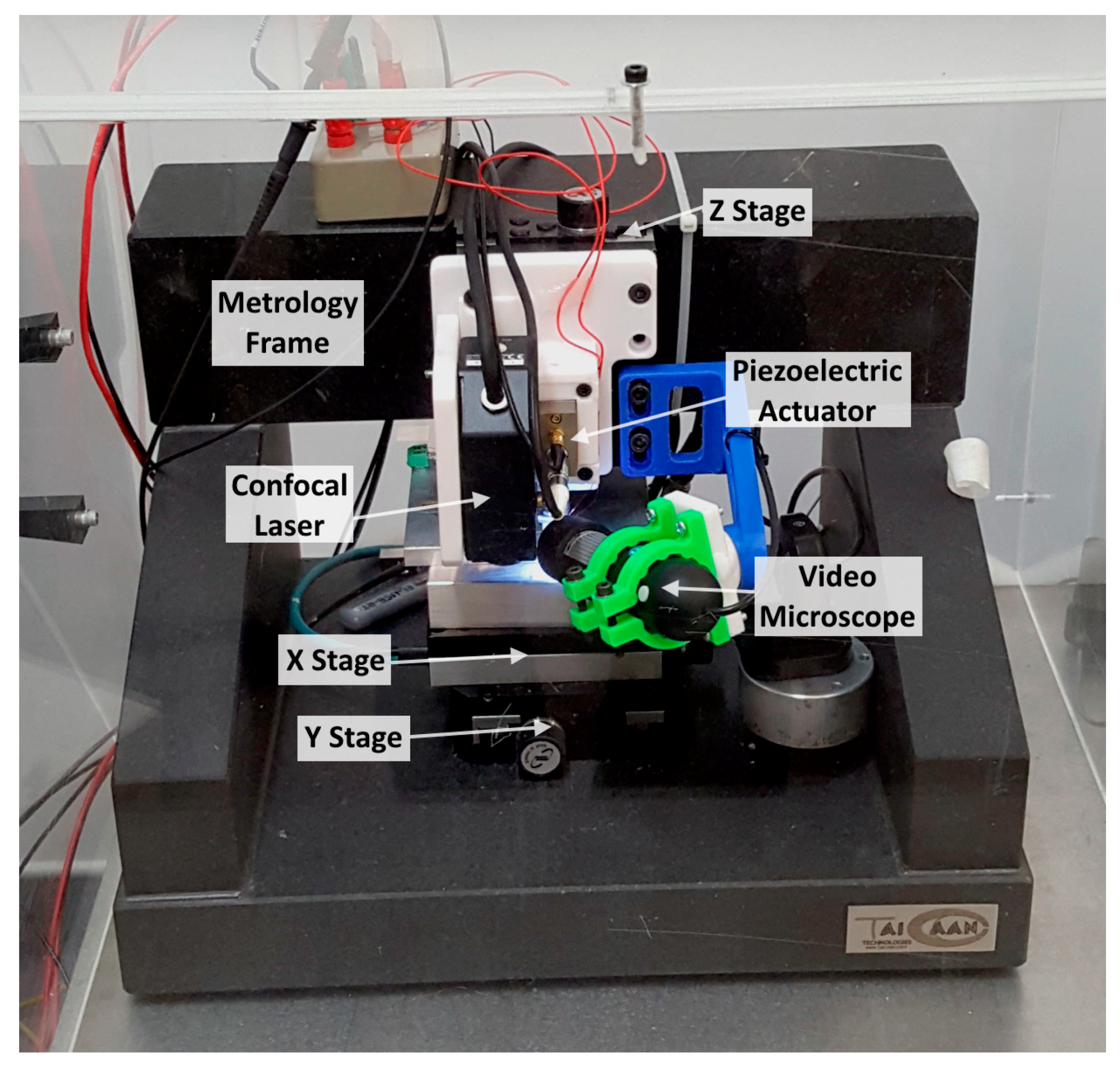
The testing apparatus allows the separation of switching contacts and the lower contact surface to be profiled using a laser displacement meter, before relocating the contacts to their original position. Figure 1 presents an overview of the main apparatus components. The apparatus consists of a granite frame that provides a fixed geometry between a lower XY motion stages and an upper Z motion stage that carries a piezoelectric actuator and displacement sensor system. The apparatus is developed from a commercial metrology system [25]. The system provides a stable metrology frame, combined with a 3D confocal laser scanning system (XYRIS 4000CL, TaiCaan Technologies Ltd., Southampton, UK), which has been modified to incorporate a MEMS switching system. In the system described a piezo electric actuator is used to directly actuate the switching mechanism. The system has been designed to also allow the incorporation of a MEMS cantilever, such that the cantilever is actuated by the piezo electric actuator, however, in this study the contact is attached directly to the actuator. The switching pair (not visible in Figure 1) is arranged with the lower contact placed level and “face-up” on the XY motion stages. The upper contact is held above the lower contact, on the tip of a piezo-electric actuator, such that raising or lowering the actuator will open or close the contact. Contact force is precisely controlled by positioning the actuator.
A 400× video microscope is used to provide visual feedback of the contact closure process.
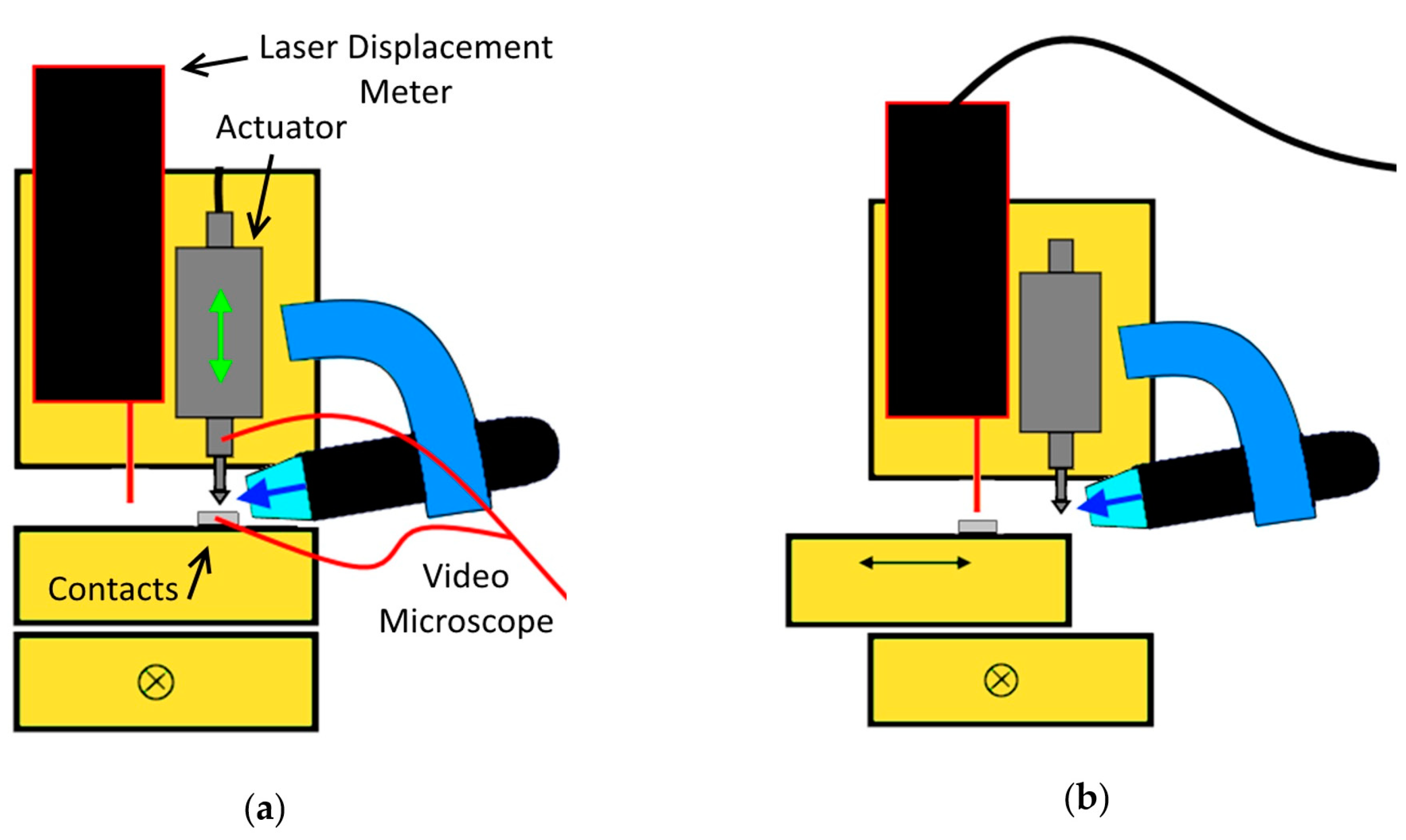
During switching (Figure 2a), the actuator (BPC301, ThorLabs, Newton, NJ, USA) moves the upper contact to open and close the contact. The actuator is capable of high speed cyclic operation (>1.25 kHz). In this study the switching cycling is interrupted after each switching operation to allow contact surface measurement.
The 3D profile of the contact surface may be measured at any point during the investigation (Figure 2b). This is performed by opening the contacts, then using the XY motion system to move the lower contact beneath a confocal laser displacement meter. The system allows placement of the contacts in a reference XYZ coordinate system to ±50 nm repeatability (XYZ positional repeatability). The laser displacement meter can resolve spatial (XY) detail at the sub-micron level on the lower contact surface with a height (Z) resolution of 10 nm. Key system specifications are summarized in Table 1.
The apparatus is mounted in a temperature-controlled metrology laboratory within a chamber to further damp thermal effects and air transmitted vibration. Temperature and humidity is continuously monitored and maintained at better than 22.0 ± 0.2 °C and 40 ± 4%RH over a 24-h period. Ground vibration isolation is by a passively damped optical-grade work surface supported by four laminar-flow air dampers (S-2000 Series, Newport Corporation, Irvine, CA, USA).
Instrumentation for data capture includes a high-speed oscilloscope (MDO4054B-3, Tektronix, Beaverton, OR, USA) to characterize the transient voltage waveform across the contact at the point of contact opening (related to the formation of the MMB), and a four terminal micro-ohmmeter (Model 580, Keithley, Cleveland, OH, USA) for contact resistance measurement under dry test conditions (<20 mV).
System measurement performance is characterized against two traceable standards. The combined noise floor of the sensor and motion system is characterized by the measurement of an optically flat target (Type 43-420-000, Edmunds Industrial Optics, Barrington, NJ, USA) over the full 25 mm × 25 mm measurement area at 125 μm intervals (40,401 evaluated points). The absolute arithmetic average (equivalent to the unfiltered Sa roughness) is then recorded. Step height accuracy is characterized by measurement of a 2660 μm step height (Model 112/557-18253, AMETEK Taylor Hobson, Leicester, UK) at 15 equally spaced intervals. The mean and standard deviation of these values is then recorded to respectively characterize the step height accuracy and the step height repeatability. The values are presented in Table 2.
2.2. Contact Manufacture
The test contacts are: (1) a hemispherical upper contact, manufactured from a 2 mm diameter precision ground stainless-steel ball, coated with a 20 nm Cr, then 500 nm Au and (2) a planar lower contact, of a SiO2 on Si substrate (N Type <100> 1000 nm Oxidised Wafer, IDB Technologies, Whitley, UK), coated with 20 nm Cr and 500 nm Au. The contact substrates are prepared by solvent cleaning (20 min ultrasound in acetone, followed by 20 min in isopropanol), and drying (blown dry with nitrogen then placed on a hot plate at 65 °C for 15 min.). They are then coated by a plasma vapor deposited 20 nm Cr adhesion promoter layer, followed by 500 nm Au conductor layer (Model SOU/150103/TPG, Kurt J Lesker, Pittsburgh, PA, USA). The Au film thickness is verified by exposing a pre-masked section on a test piece which is then measured for the film step height using the XYRIS 4000CL.
2.3. Test Circuit
The circuit configurations for switching and contact resistance measurement are shown in Figure 3. The contact resistance is measured by the 4-terminal method using a micro-ohmmeter (Model 580, Keithley, Cleveland, OH, USA) Figure 3a. The switching circuit is a simple series loop incorporating a 4 V battery with current controlled by a resistive load—Figure 3b.
2.4. Contact Force Determination
The applied contact force is controlled by bringing the contacts to the point of just meeting, and then demanding further extension of the actuator. As the actuator continues to be extended the contact closure force increases. The ICE apparatus as presented does not include a transducer to directly measure force. To determine the contact force a second apparatus is used [26], to calibrate the relationship between the initial applied force and the contact resistance for the contact samples. In the ICE apparatus a new undamaged surface contact resistance is thus linked to the calibrated force. The actuator displacement to contact force relationship is derived from the contact pair resistance/force curve measured by a four terminal micro-ohmmeter (Model 580, Keithley, Cleveland, OH, USA) and piezo force sensor (Model 9207, Kisler AG, Winterthur, Switzerland) in the Holm crossed bar configuration with apparatus previously described in [26].
2.5. Switching Test Procedure
The initial contact closure position for the test is obtained by slowly closing the contacts until they are in close proximity (shown in Figure 4). The contacts are then pushed together by the actuator until the contact resistance is reached that corresponds to the normal contact force required for the test. The actuator position is repeated for subsequent cycles. The contact is held stationary for 30 s to allow the contact interface to settle before the contact resistance measurement is recorded. The load circuit is then connected, and current is allowed to flow for 10 s before contact opening to a separation of 0.1 mm is demanded at a maximum acceleration of 100 mm/s2. The load circuit is then disconnected, and the lower contact measured by the laser displacement meter. After contact surface measurement the contacts are repositioned to the original coordinates and the process repeated.
2.6. Surface Measurement Analysis
The lower contact surface measurements are evaluated for surface roughness and volume wear (Boddies 3D v2.18, TaiCaan Technologies, Southampton, UK). The lower contact surface wear is measured under two conditions and these are summarized in Table 3.
3. Results
3.1. Contact Force and Demanded Actuator Displacement vs. Contact Resistance
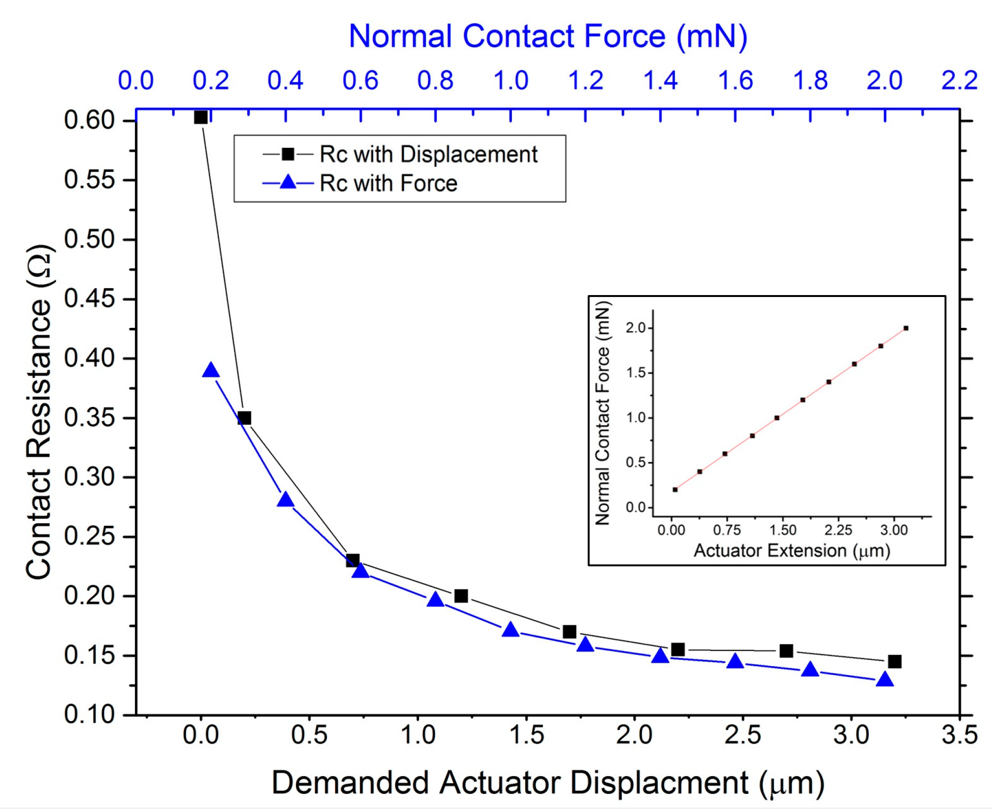
Figure 4 shows the contact resistance to contact force and demanded contact displacement and contact force. The new apparatus allowed the contacts to be positioned to achieve a stable contact resistance of 0.6012 Ω. The lowest stable contact force that could be measured with the force testing apparatus was at 200 μN at a contact resistance of 0.3808 Ω. The inset figure shows the relationship between the extension demanded from the actuator and the contact force.
Over the range of measured force to contact resistance (200 to 2000 μN) there is good agreement between the displacement and force curves. This provides a range of contact resistance between ~0.15 and 0.60 Ω where the relationship between actuator displacement and contact force is linear, as shown in Figure 5. This allows contact resistance to be used to determine the initial contact force.
3.2. Cold Switched Contact Sequence
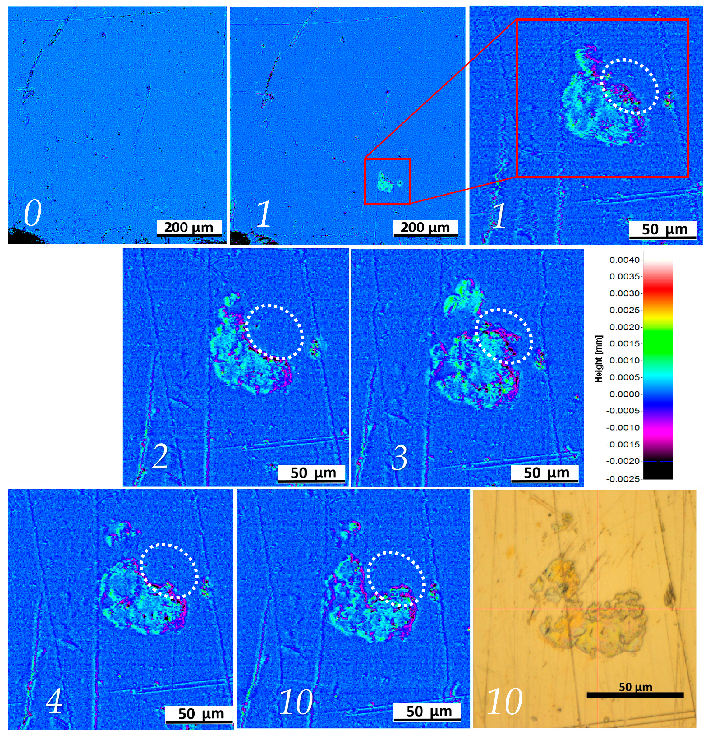
The evolution of the cold switched contact surface over 10 cycles at ~100 µN is presented in Figure 6. The surface height is represented by a colour scale set to the same height range (+4.0 to −2.0 µm) for each panel in Figure 6 to provide a fixed reference for visual inspection. The contact surface is measured before switching (0 cycles) over an area of 0.7 mm by 0.7 mm, but a smaller and more detailed measurement of 0.15 mm by 0.15 mm is taken of the precise contact location following the first switch cycle. The number of switching cycles the surface has experienced is shown in the lower left corner i.e., 0 is before any switching.
Figure 6 shows a pattern raised above the nominal surface that is approximately 50 µm in diameter and appears after a single switching operation (from 0 to 1 cycles). The pattern presents as a roughened, raised region approximately 500 nm above the nominal contact surface, with an irregular circular shape. Following the completion of the switching sequence the contact region is imaged with true colour optical video microscopy. The shape of the site is well correlated between the micrograph image and the final measurement of the wear site with the micrograph showing the wear region to be gold colored (cycle 10).
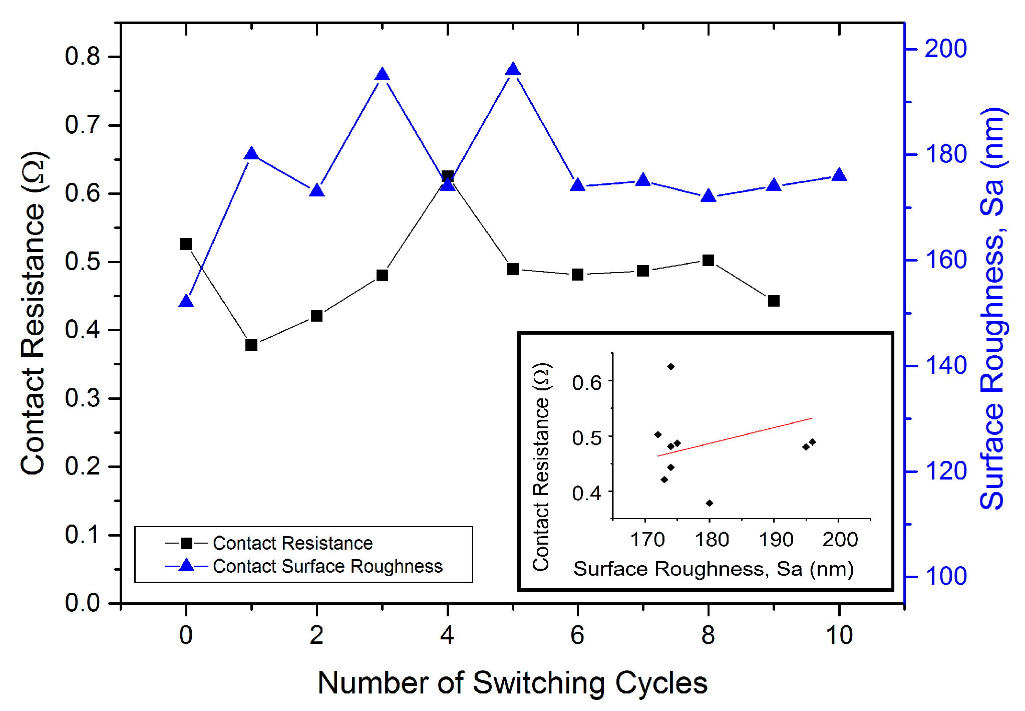
The progression of the contact resistance and lower surface roughness is shown against the number of switching cycles in Figure 7 with a subplot of contact resistance against surface roughness.
The contact resistance and surface roughness are shown to be initially unstable between cycles before stabilizing after five cycles. The inset figure shows a trend for the contact resistance to increase with the surface roughness.
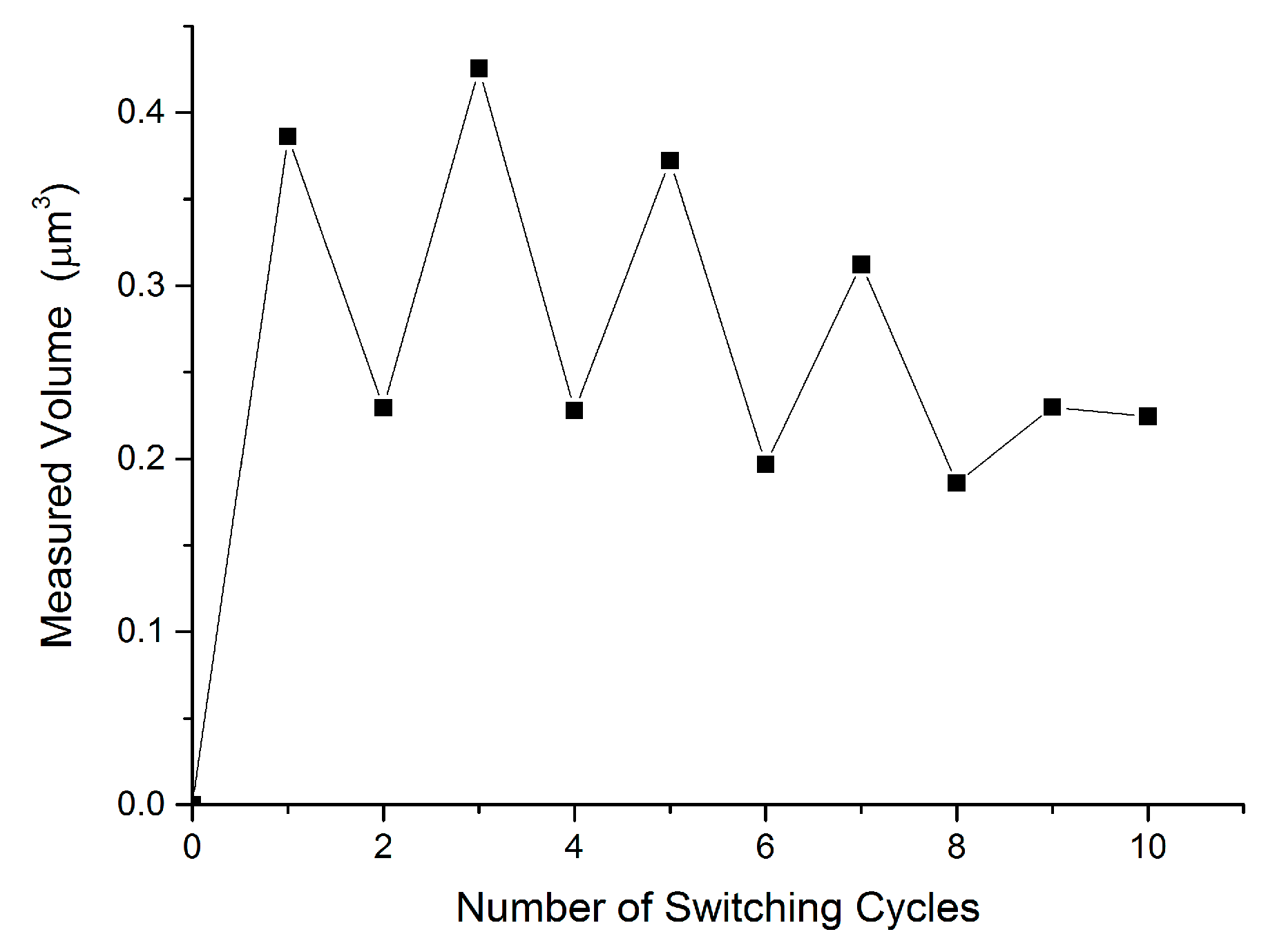
The volume of material above the nominal surface of the lower contact before switching is evaluated from the surface measurements on a cycle-by-cycle basis and presented in Figure 8 [27]. The datum of zero volume transfer (0) is defined as the volume measured above the plane of best fit to the unswitched contact surface. A positive volume indicates there has been net surface deposition upon the contact surface. It is apparent from Figure 8 that after the first cycle 0.38 µm3 of material has been deposited on the surface, after the second cycle the deposited volume has reduced to 0.22 µm3 but following the third cycle increases to 0.43 µm3. Figure 6 shows that the top right region of the deposit (enclosed by a dashed white oval) appears to be transferred back and forth between contacts. Figure 8 shows that the volume transferred back and forth each cycle is reducing over the following 10 cycles with the smallest volume of material transfer occurring between the final switching cycles. After 10 cycles there is a net positive volume deposited of ~0.22 μm3.
3.3. 20 mA 4 V Direct Current (DC) Hot Switched Contact Sequence
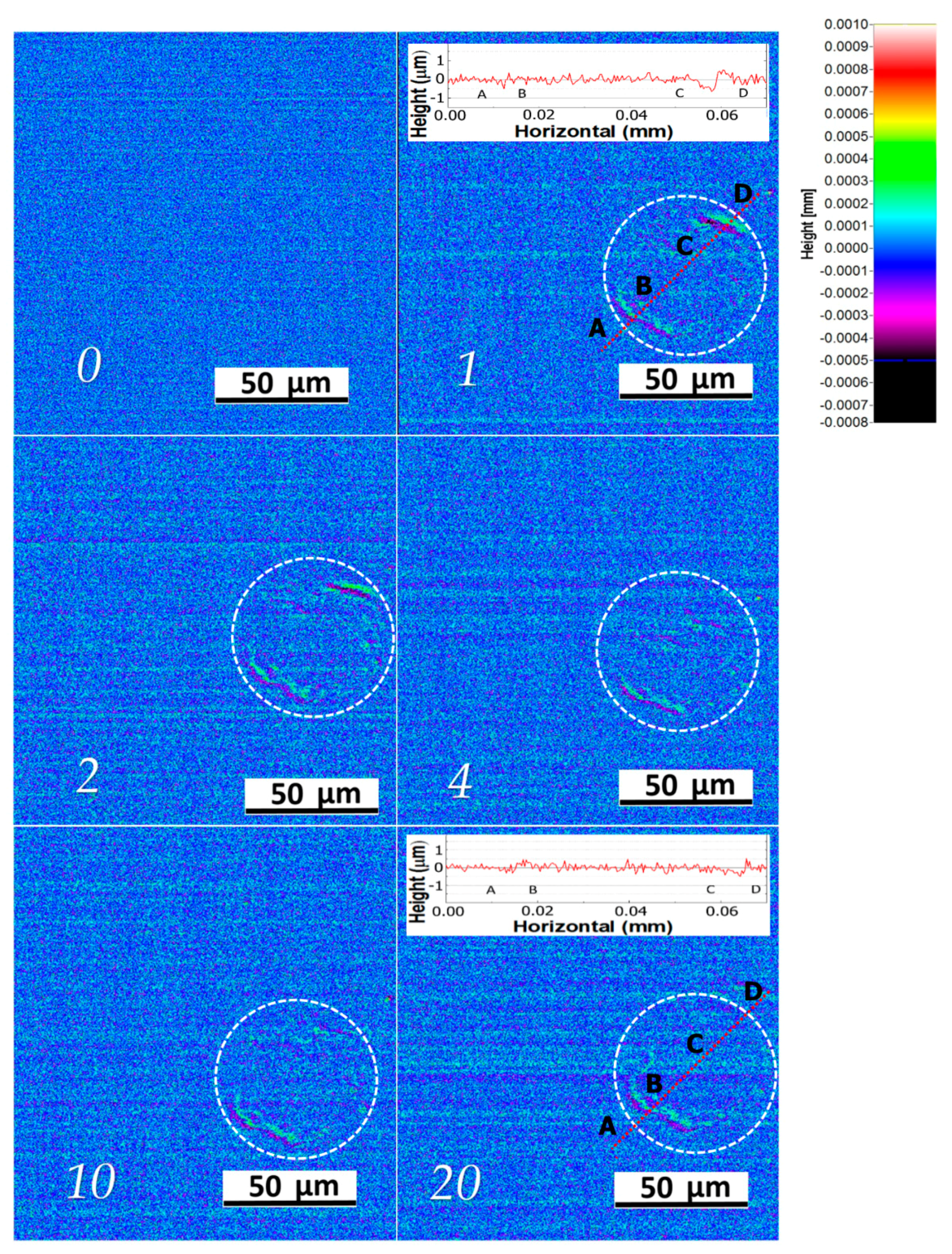
The evolution of a hot switched contact surface over 20 cycles at ~500 µN is presented in Figure 9. The measurement area is 150 μm by 150 μm. The surface height is represented by a colour scale set to the same height range for each panel in Figure 9 (+1.0 to −0.5 µm). It should be noted that the range of this scale is one quarter of that used in Figure 6 to better enhance the subtle surface features in this sequence. A white dashed ring is used to indicate the wear region, with the features of note labelled AB and CD. A cross section of the surface along the red dotted line is presented after 1 and 20 cycles.
Figure 9 shows the contact surface at 0 cycles (before switching) and after 1, 2, 4, 10, and 20 cycles. The wear pattern presents as a toroidal region approximately 45 μm in outer diameter, highlighted by a dashed circular line, with the most significant change in surface height occurring after 1 and 2 cycles in the lower left (AB), and upper right (CD) of this region. The surface colour map shows the lowest area to be ~500 nm below the nominal surface (purple areas) with the highest area immediately alongside and ~500 nm above the nominal surface (green areas). Features AB and CD appear to be tears in the Au film, with the film lifting off the Si substrate at the edges of the tear.
After four switched cycles the height and width of the tears appear to both decrease in magnitude and begin to smooth, particularly in the CD region of the wear pattern where the surface height stabilizes. This smoothing trend continues until the completion of switching after 20 cycles.
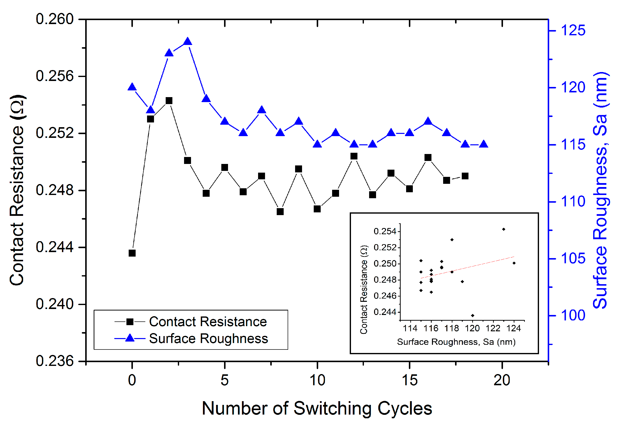
The evolution of the lower contact surface roughness and the contact resistance is presented in Figure 10 along with a subplot showing the relationship between contact resistance and surface roughness. Both roughness and resistance show an initial rise over the first switching cycles before settling between cycles 5 to 20. After cycle 5 there is a trend of the surface roughness decreasing while contact resistance is broadly stable.
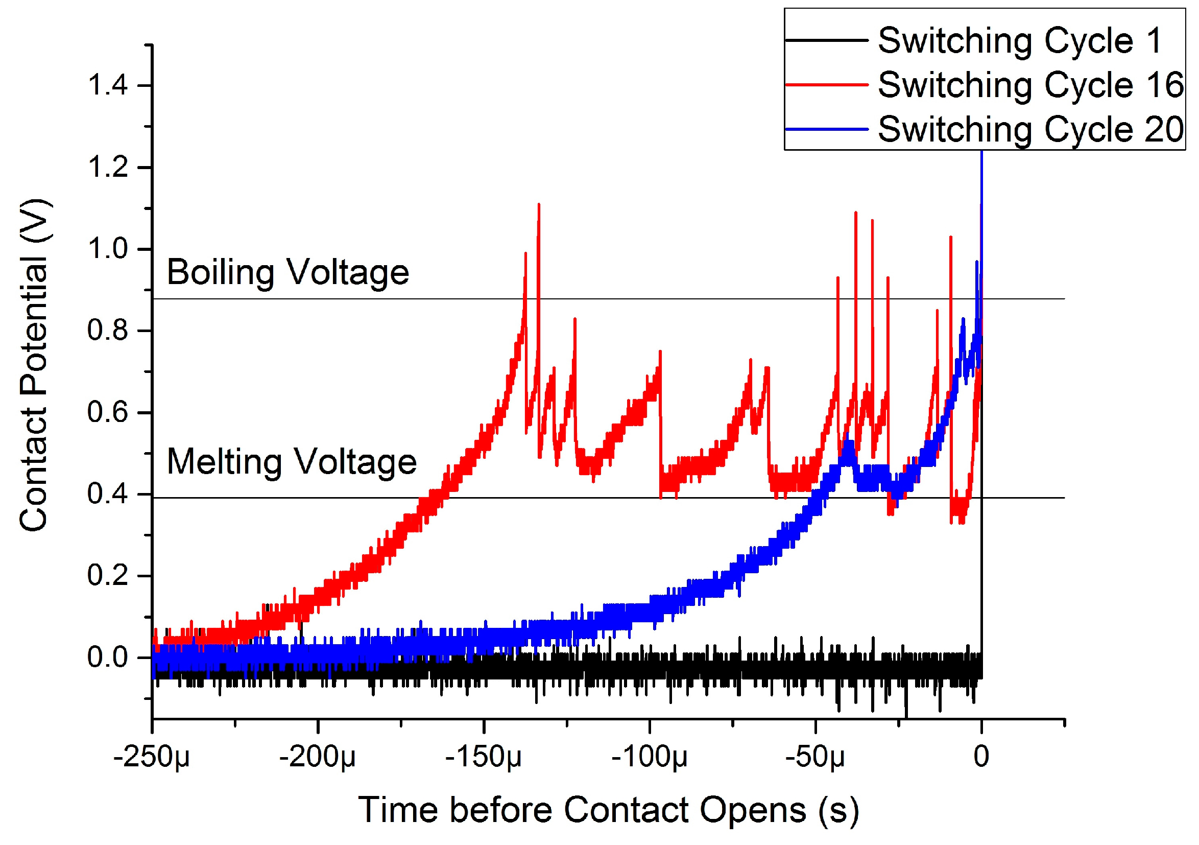
The voltage waveform at the point of contact opening is captured at each cycle of switching. Two types of waveform are observed with examples shown in Figure 11. The first is a less stable and unrepeatable event where the contact potential is observed to vary between ~0.4 and 0.9 V before finally rising abruptly to the full open circuit potential—termed “MMB” (molten metal bridge) type. The MMB type occurs as the gradual reduction in the contact area constricts current flow leading to increased Joule heating and the local softening, melting and boiling of the contact surface at the contacting asperities. The second type of waveform observed is an abrupt and instantaneous rise in contact potential to the full open circuit voltage. We term this waveform here a “delamination” type.
Figure 11 shows the 1st, 16th and 20th opening waveforms as examples of the types of waveform. The 1st cycle (black) shows the abrupt “delamination” waveform suggests that as a MMB event is not observed the contact area has not decreased gradually, but rather has separated suddenly.
The longer waveforms (16th—red and 20th—blue) are typical of the MMB phenomenon, where the gradual reduction in contact area causes the microscale melting and boiling of the contact surface and the contact opens as the molten bridge ruptures by boiling and cannot reform. The reported voltages for the melting and boiling of Au (~0.38 and ~0.88 V respectively) are plotted for comparison. [19,28].
Each switching waveform is classified for the type of opening as either a “delamination” or “MMB” type, with four events classified as “delamination” type and 16 as “MMB”. The waveform type is then compared to the magnitude of surface roughness change before and after the opening event.
The 1st, 2nd, 4th and 14th opening event are of the “delamination” type. Figure 9 shows the surface of the contact after the 1st, 2nd and 4th cycles suggest the Au film is tearing and lifting from the substrate at AB and CD. It was found that while an MMB event was associated with a change in surface roughness of 1.06 nm, a delamination event had a much greater average change of 3.25 nm.
4. Discussion
4.1. Cold Switched Contact Sequence
The contact resistance, surface roughness (Figure 7), volume transfer (Figure 8) and surface imagery (Figure 6) all suggest that the contact pair experienced a delamination of the Au film from the upper hemispherical contact during the first switching cycle. Some of this material was then transferred back and forth between the contacts with the volume of transfer decreasing with continued cycles, shown in Figure 8. The initial phase of switching is well known to demonstrate a gradual decrease in contact resistance as the surfaces begin to conform to one another and “bed in”. Laurvick et al. also observe the initial phase of switching with Au-Au MEMS contacts coincides with the greatest variation in contact resistance during the switching lifetime, however, they also noted that where the decrease in contact resistance was not smooth and gradual it correlated with the premature failure of the device [4]. The observed delamination presents a significant defect in the contact surface that can reasonably be expected to lead to premature contact failure. The observation in this study of a delamination effect linked to unstable contact resistance suggests a mechanism for the premature failures observed in [4]. The trend observed between increasing roughness and contact resistance (Figure 7) supports this. As the surface volume change stabilizes the contact resistance is also stabilized, but at a higher level than the 0.45 Ω measured at the initial closure on the undamaged interface, suggestive that the change in surface texture is at least partially responsible. As the material transfer is reduced, the contact interface will evidently be more stable, and therefore the contact resistance also stabilizes. This suggests the Au film is has at least partially re-adhered to the ball. Jensen et al. observed the adhesive forces between Au-Au MEMS switches were dependent on both adhesive forces between surfaces in the apparent contact area but of also by the metal-metal adhesion in the real contact area [29]. With the contact resistance primarily dependent on the real contact area any change in adhesion between contacts cannot be inferred from the contact resistance alone. It is noted that the observed detachment of the Au film from the substrate will allow significantly increased rates of strain in the film and thus an increased rate of strain-hardening. This may be a contributory factory to the increased contact resistance as a harder contact material that evidently provides a smaller contact area for a given force.
Adhesion in Au contacts is a recognized problem and this presents a significant failure mechanism for the MEMS switch, particularly when the poor adhesion of Au to Si/SiO substrates is considered. In this study an adhesion promoter (Cr) was used, previously demonstrated by Lewis et al., to enhance switching lifetimes in Au contacts [30]. However, while this study was carried out under controlled temperature and humidity, the test environment was not under hermetic seal or inert gas, and the presence of water vapor and hydrocarbon contamination is expected. These are both recognized as factors in influencing the self-adhesion of Au, an effect that would be reduced in a practical Au thin-film device by sealing under an inert atmosphere [29,31]. However, the intention of future work is investigating a novel contact material, capable of operating without hermetic encapsulation and offering the potential for reducing the potential for complications that arise from this process [32]. In this context this study provides a useful bench mark for Au film behavior in an ambient atmospheric environment for future investigation.
4.2. Hot Switched Contact Sequence 20 mA
A wear scar appears after a single switching event that is described by a toroid where the thin-film surface shows partial tearing and wrinkling at opposing sides (Figure 9, cycles 1 and 2). The height of the features AB and CD shown in Figure 9 are ~500 nm. As this is the deposited Au film thickness it suggests that the film has torn, delaminated from the substrate and shifted laterally to expose the Si wafer. The toroidal wear shape is significant as it has been previously shown analytically and empirically that the maximum current density occurs preferentially at the edges of the contact region [6,33]. The visual representation of the surface height in Figure 9 show the greatest change occurring at the 1st, 2nd, and 4th cycles at the AB and CD features. The voltage waveform observed at these cycles was not representative of a molten metal bridge event and suggests the contact area has not decreased gradually, but suddenly. The change in surface roughness associated with this “delamination” type waveform is over three times higher than what was observed for the molten metal bridge type.
Cross sections comparing the AB and CD features in Figure 9 after the 1st and 20th cycle show they have reduced in scale after 20 cycles. The trend of decreasing surface roughness is also seen in Figure 10 from the 5th to 20th switching cycle onwards. The 14th cycle shows a small increase in roughness and this is the final “delamination” type voltage waveform. It appears that the feature at CD is a tear in the Au film that is gradually closed as switching continues. During the initial phase of switching it is apparent that the local contact pressure in the real area of contact will be higher as the most prominent surface asperities in contact undergo plastic deformation and additional surrounding asperities begin to distribute the contact load more elastically as the contacts “bed in” [4,6]. It is during this initial phase where the higher local pressures and plastic deformation are most likely to result in cold welding. The observation of the delamination waveforms occurring in early switch operations (1st, 2nd and 4th) suggests a correlation with the period of highest plastic deformation. A recent study has shown that hot switched MEMS contact welding is observed regularly at conditions of 10 V DC and 80 mA, and sporadically at 10 V DC and 60 mA, however, the study did not specify the contact closure force, and the reported contact resistance suggests it was higher than this study [34].
As the switching sequence continues, it is apparent from Figure 9 that the tear in the thin-film Au observed at the CD feature of the contact region is visibly reduced and appears to be smoothed out. The smoothing effect is confirmed by the progression of roughness from the 5th switching cycle (Figure 10). The surface roughness and contact resistance decrease, with all but one of the last 15 opening waveforms characterized by MMB type events. The observations of Laurvick et al., that over long term switching the irregular progression of contact resistance correlated to premature device failure [4] is noted, as in this study the largest changes in contact resistance correlated with the largest changes in surface texture and the appearance of apparent tears in the Au film.
These observations suggest the delamination events are associated with a higher level of damage to the Au film, while the MMB type events correlate to decreased damage, film smoothing and perhaps even repair of the film.
5. Conclusions
The purpose of this investigation was to describe, outline and test the capabilities of a novel MEMS apparatus for the measurement of In-situ Contact Evolution. The ICE apparatus is demonstrated to resolve detail of microscopic wear occurring in-situ at the contact interface under low force conditions. The results show that the apparatus is capable of detection of wear in both cold (dry switching) and hot switching from the first cycling of the contacts.
During the first 20 cycles of a hot switched (20 mA, 4 V) Au contact at MEMS scale closure force, it is shown that there are opening events with no apparent MMB. The opening event is characterized by a step change in the voltage across the device (sampled at 25 MHz) and linked to a quantifiably greater surface roughness change than the MMB event. This paper defines these as delamination events (DE). The ICE apparatus shows for the first time that these events result from the cold welding of the Au layers, and the subsequent tearing of the surface (delamination). It is interesting to note that the tearing of the surface film seems to prevent a MMB.
Author Contributions
Conceptualization, J.W.M.; Methodology, T.G.B.; Validation, J.W.M. and T.G.B.; Formal Analysis, T.G.B.; Investigation, T.G.B.; Writing-Original Draft Preparation, T.G.B.; Writing-Review & Editing, T.G.B. and J.W.M.; Supervision, J.W.M.; Project Administration, J.W.M.; Funding Acquisition, J.W.M.
Funding
This research was funded by the Engineering and Physical Sciences Research Council (EPSRC) grant number EP/M508147/1.
Acknowledgments
The authors would like to thank Kevin J. Cross from TaiCaan Technologies Ltd. for his assistance in the development of the apparatus control.
Conflicts of Interest
The authors declare no conflict of interest.
References
- Rebeiz, G.M. RF MEMS: Theory, Design, and Technology; John Wiley & Sons: Hoboken, NJ, USA, 2004. [Google Scholar]
- Iannacci, J. RF-MEMS: An enabling technology for modern wireless systems bearing a market potential still not fully displayed. Microsyst. Technol. 2015, 21, 2039–2052. [Google Scholar] [CrossRef]
- Toler, B.F.; Coutu, R.A.; McBride, J.W. A review of micro-contact physics for microelectromechanical systems (MEMS) metal contact switches. J. Micromech. Microeng. 2013, 23, 103001. [Google Scholar] [CrossRef]
- Laurvick, T.V.; Coutu, R.A. Improving gold/gold microcontact performance and reliability under low-frequency ac through circuit loading. IEEE Trans. Compon. Packag. Manuf. Technol. 2017, 7, 345–353. [Google Scholar] [CrossRef]
- Yunus, E.M.; McBride, J.W.; Spearing, S.M. The relationship between contact resistance and contact force on au-coated carbon nanotube surfaces under low force conditions. IEEE Trans. Compon. Packag. Technol. 2009, 32, 650–657. [Google Scholar] [CrossRef]
- Holm, R. Electric Contacts: Theory and Application; Springer Science & Business Media: Berlin, Germany, 1958. [Google Scholar]
- Hyman, D.; Mehregany, M. Contact physics of gold microcontacts for mems switches. In Proceedings of the Forty-Fourth IEEE Holm Conference on Electrical Contacts, Arlington, VA, USA, 26–28 October 1998; IEEE: New York, NY, USA, 1998; pp. 133–140. [Google Scholar]
- Gouldstone, A.; Koh, H.-J.; Zeng, K.-Y.; Giannakopoulos, A.; Suresh, S. Discrete and continuous deformation during nanoindentation of thin films. Acta Mater. 2000, 48, 2277–2295. [Google Scholar] [CrossRef]
- Jensen, B.D.; Huang, K.; Chow, L.L.W.; Kurabayashi, K. Low-force contact heating and softening using micromechanical switches in diffusive-ballistic electron-transport transition. Appl. Phys. Lett. 2005, 86, 023507. [Google Scholar] [CrossRef] [Green Version]
- Zhang, P.; Lau, Y.; Timsit, R.S. On the spreading resistance of thin-film contacts. IEEE Trans. Electron. Dev. 2012, 59, 1936–1940. [Google Scholar] [CrossRef]
- Coutu, R.A.; McBride, J.W.; Starman, L.A. Improved micro-contact resistance model that considers material deformation, electron transport and thin film characteristics. In Proceedings of the 55th IEEE Holm Conference on Electrical Contacts, Vancouver, BC, Canada, 14–16 September 2009; IEEE: New York, NY, USA, 2009. [Google Scholar]
- Malucci, R.D. The impact on current density and constriction resistance from bridge structures in real contacts. In Proceedings of the 2017 IEEE Holm Conference on Electrical Contacts, Denver, CO, USA, 10–13 September 2017; IEEE: New York, NY, USA; pp. 59–62. [Google Scholar]
- Fukuyama, Y.; Sakamoto, N.; Kaneko, N.-H.; Kondo, T.; Toyoizumi, J.; Yudate, T. The effect of the distribution of α-spots in the peripheral part of an apparent contact point on constriction resistance. In Proceedings of the 2017 IEEE Holm Conference on Electrical Contacts, Denver, CO, USA, 10–13 September 2017; IEEE: New York, NY, USA; pp. 302–305. [Google Scholar]
- Liu, H.; McBride, J.W. The influence of multiscale surface roughness on contact mechanics using finite element modeling: Applied to a au-coated cnt composite electrical contact surface. In Proceedings of the 2017 IEEE Holm Conference on Electrical Contacts, Denver, CO, USA, 10–13 September 2017; IEEE: New York, NY, USA; pp. 229–235. [Google Scholar]
- Lewis, A.P.; McBride, J.W.; Jiang, L. Evolution of voltage transients during the switching of a mems relay with au/mwcnt contacts. IEEE Trans. Compon. Packag. Manuf. Technol. 2015, 5, 1747–1754. [Google Scholar] [CrossRef]
- Mcbride, J.; Yunas, E.; Spearing, S. Gold coated carbon nanotube surfaces as low force electrical contacts for mems devices: Part 1. In Proceedings of the 59th IEEE Holm Conference on Electrical Contacts, Newport, RI, USA, 14–16 September 2009. [Google Scholar]
- Ren, W. Unstable electrical contact behaviour at nanoscale for mems switch. In Proceedings of the 28th International Conference on Electric Contacts, Edinburgh, UK, 6–9 June 2016; pp. 213–218. [Google Scholar]
- Stilson, C.; Coutu, R. Contact resistance evolution of highly cycled, lightly loaded micro-contacts. In Proceedings of the SPIE MOEMS-MEMS 2014, San Francisco, CA, USA, 1–6 February 2014; International Society for Optics and Photonics: San Francisco, CA, USA. [Google Scholar]
- Doduco. Databook of Electrical Contacts; Duduco GmbH: Pforzheim, Germany, 2012. [Google Scholar]
- Koren, P.; Nahemow, M.; Slade, P. The molten metal bridge stage of opening electrical contacts. IEEE Trans. Parts Hybrids Packag. 1975, 11, 4–10. [Google Scholar] [CrossRef]
- McBride, J. The wear processes of gold coated multi-walled carbon nanotube surfaces used as electrical contacts for micro-electro-mechanical switching. Nanosci. Nanotechnol. Lett. 2010, 2, 357–361. [Google Scholar] [CrossRef]
- Bull, T.; Mcbride, J. The influence of circuit parameters on molten metal bridge energy in a mems relay testing platform. In Proceedings of the 2016 Twenty Eighth International Conference on Electrical Contacts, Edinburgh, UK, 6–9 June 2016. [Google Scholar]
- Leach, R.E. Optical Measurement of Surface Topography; Springer: Berlin, Germany, 2011. [Google Scholar]
- Nouira, H.; El-Hayek, N.; Yuan, X.; Anwer, N.; Salgado, J. Metrological Characterization of Optical Confocal Sensors Measurements (20 and 350 Travel Ranges); Journal of Physics: Conference Series; IOP Publishing: Bristol, UK, 2014; p. 012015. [Google Scholar]
- Taicaan Technologies Xyris 4000. Available online: http://www.taicaan.com/xyris-4000/ (accessed on 29 March 2018).
- McBride, J.; Jiang, L.; Chianrabutra, C. Fine transfer in electrical switching contacts using gold coated carbon-nanotubes. In Proceedings of the 26th International Conference on Electrical Contacts (ICEC 2012), Beijing, China, 14–17 May 2012; IET: Beijing, China; pp. 353–358. [Google Scholar]
- Mcbride, J.W. A review of volumetric erosion studies in low voltage electrical contacts. IEICE Trans. Electron. 2003, 86, 908–914. [Google Scholar]
- Slade, P.G. Electrical Contacts: Principles and Applications, 2nd ed.; CRC Press: Boca Raton, FL, USA, 2014. [Google Scholar]
- Jensen, B.D.; Huang, K.W.; Chow, L.L.W.; Kurabayashi, K. Adhesion effects on contact opening dynamics in micromachined switches. J. Appl. Phys. 2005, 97, 103535. [Google Scholar] [CrossRef]
- Lewis, A.; Down, M.; Chianrabutra, C.; Jiang, L.; Spearing, S.; McBride, J. The effect on switching lifetime of chromium adhesion layers in gold-coated electrical contacts under cold and hot switching conditions. In Proceedings of the 2013 IEEE 59th Holm Conference on Electrical Contacts (HOLM), Newport, RI, USA, 22–25 September 2013; IEEE: New York, NY, USA, 2013; pp. 1–7. [Google Scholar]
- Cognard, J. Adhesion to gold: A review. Gold Bull. 1984, 17, 131–139. [Google Scholar] [CrossRef]
- Spearing, S.M. Materials issues in microelectromechanical systems (MEMS). Acta Mater. 2000, 48, 179–196. [Google Scholar] [CrossRef]
- Sawada, S.; Tsukiji, S.; Shimada, S.; Tamai, T.; Hattori, Y. Current density analysis of thin film effect in contact area on led wafer. In Proceedings of the 58th Holm Conference on Electrical Contacts, Portland, OR, USA, 23–26 September 2012; IEEE: New York, NY, USA; pp. 1–6. [Google Scholar]
- Lisec, T.; Stoppel, F.; Kaden, D.; Heinrich, F.; Neumann, A.; Wagner, B. MEMS switch with prolonged lifetime under hot switching conditions based on gold as contact material. In Proceedings of the 2017 19th International Conference on Solid-State Sensors, Actuators and Microsystems (TRANSDUCERS), Kaohsiung, Taiwan, 18–22 June 2017; IEEE: New York, NY, USA; pp. 2043–2046. [Google Scholar]
Figure 1.
The In-situ Contact Evolution (ICE) apparatus, based on a XYRIS 4000CL, TaiCaan Technologies, Southampton, UK. The lower contact is carried on the XY motion system, while the upper contact is carried on the lower tip (obscured by video microscope) of the piezoelectric actuator.
Figure 1.
The In-situ Contact Evolution (ICE) apparatus, based on a XYRIS 4000CL, TaiCaan Technologies, Southampton, UK. The lower contact is carried on the XY motion system, while the upper contact is carried on the lower tip (obscured by video microscope) of the piezoelectric actuator.

Figure 2.
Schematic of In-site Surface Evolution (ICE) testing apparatus during (a) Switching Mode, where the piezo-electric actuator opens and closes the switch and (b) Surface measurement mode.
Figure 2.
Schematic of In-site Surface Evolution (ICE) testing apparatus during (a) Switching Mode, where the piezo-electric actuator opens and closes the switch and (b) Surface measurement mode.

Figure 3.
(a) Contact Resistance Measurement Circuit and (b) Contact Load Circuit.
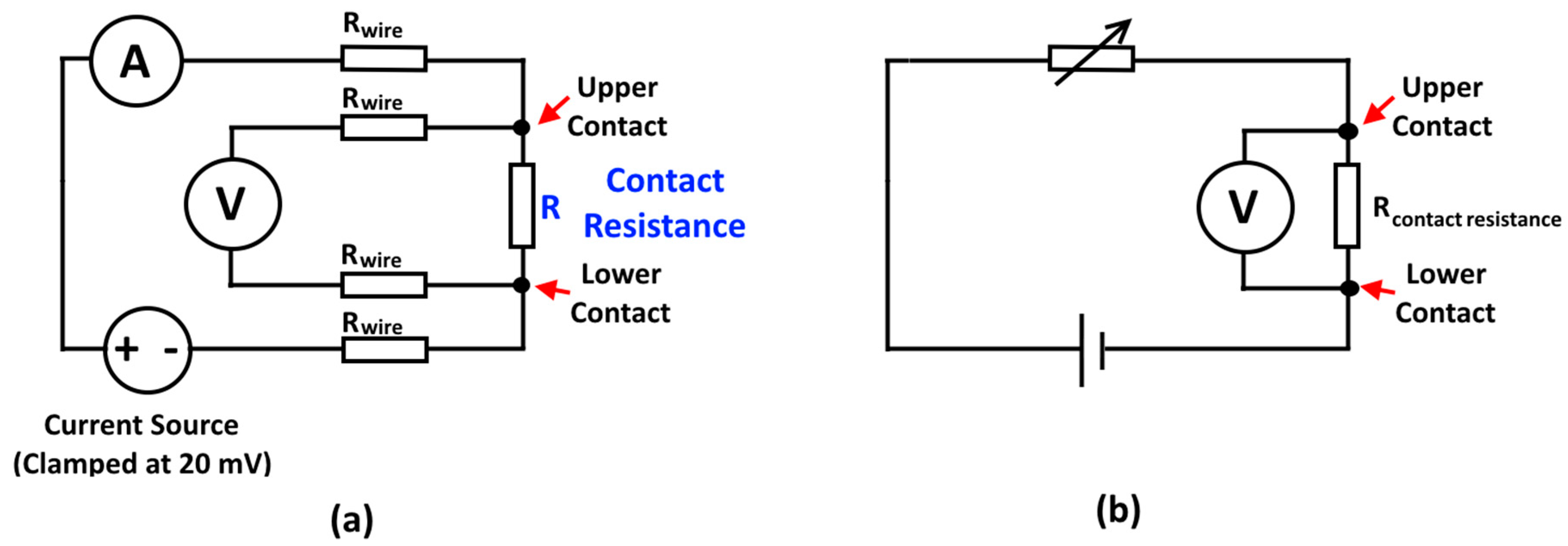
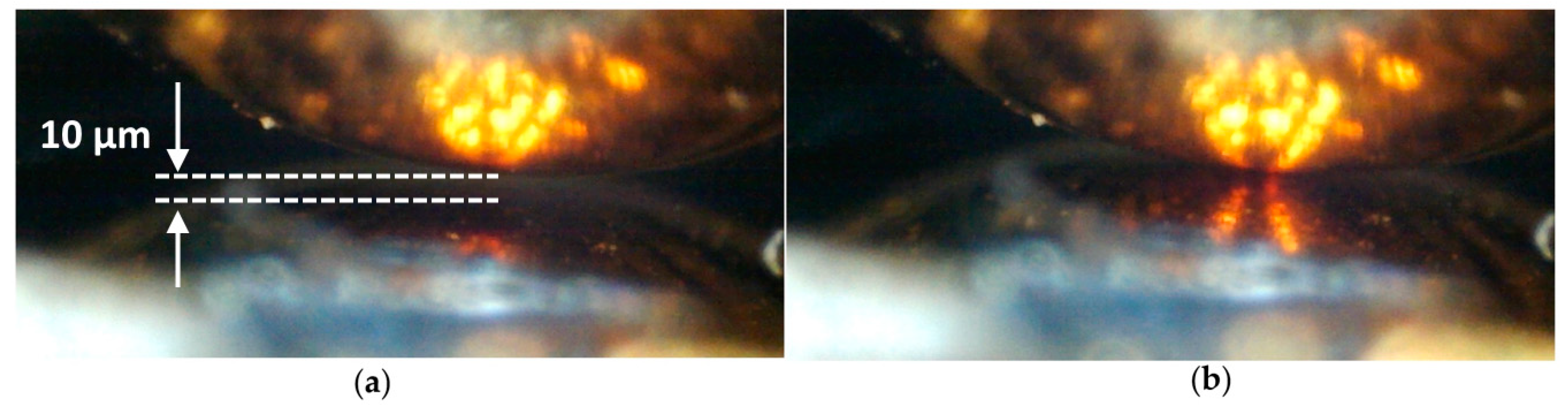
Figure 4.
The contact pair shown through the 400× integrated video microscope (a) with a 10 μm separation between contacts and (b) in contact.
Figure 4.
The contact pair shown through the 400× integrated video microscope (a) with a 10 μm separation between contacts and (b) in contact.

Figure 5.
Contact Resistance to Contact Force (blue triangles), and Contact Resistance to Contact Demanded Displacement (black squares) with Contact Force to Actuator Displacement (inset).
Figure 5.
Contact Resistance to Contact Force (blue triangles), and Contact Resistance to Contact Demanded Displacement (black squares) with Contact Force to Actuator Displacement (inset).

Figure 6.
A sequence of measurements of the lower contact during a cold switching sequence at 100 μN normal contact force. At 0 (before switching), 1, 2, 3, 4 and 10 cycles. The white dotted region shows an unstable region of deposition.
Figure 6.
A sequence of measurements of the lower contact during a cold switching sequence at 100 μN normal contact force. At 0 (before switching), 1, 2, 3, 4 and 10 cycles. The white dotted region shows an unstable region of deposition.

Figure 7.
The evolution of contact resistance and surface roughness over 10 cold switching cycles.

Figure 8.
The evolution of material deposited on the lower contact surface over 10 cold switching cycles.
Figure 8.
The evolution of material deposited on the lower contact surface over 10 cold switching cycles.

Figure 9.
A sequence of measurements of the lower contact during a hot 20 mA 4 V Direct Current (DC) switching sequence at 500 μN normal contact force. 0.15 mm × 0.15 mm region after 0, 1, 2, 4,10 and 20 cycles.
Figure 9.
A sequence of measurements of the lower contact during a hot 20 mA 4 V Direct Current (DC) switching sequence at 500 μN normal contact force. 0.15 mm × 0.15 mm region after 0, 1, 2, 4,10 and 20 cycles.

Figure 10.
The evolution of contact resistance and surface roughness over 20 hot switched 4 V Direct Current (DC) 20 mA switching cycles.
Figure 10.
The evolution of contact resistance and surface roughness over 20 hot switched 4 V Direct Current (DC) 20 mA switching cycles.

Figure 11.
Contact Potential immediately before contact opening showing MMB and delamination type openings.
Figure 11.
Contact Potential immediately before contact opening showing MMB and delamination type openings.


Table 1.
Summary of key specifications of the In-situ Contact Evolution (ICE) apparatus.
| Measurement Principle | Vertical (Z) Resolution | Vertical Range | XY Range | XY On-Axis Repeatability | Sensor Light Source | Sensor Spatial (XY) Resolution |
|---|---|---|---|---|---|---|
| Point Autofocus | 10 nm | 0.6 mm | 25 mm × 25 mm | ±50 nm | 655 nm (Red Laser) | <1 µm |
Table 2.
Summary of key system performance on traceable standards.
| Noise Floor (Optically Flat Standard) Sa | Step Height Accuracy (2660 µm Standard) Mean | Step Height Repeatability (2660 µm Standard) Standard Deviation |
|---|---|---|
| 24.2 nm | 2660 µm | 32 nm |
Table 3.
Circuit and Force Conditions for each switching sequence.
| Test Condition | Circuit Voltage (V) | Circuit Current (mA) | Contact Force (µN) | Number of Switching Cycles |
|---|---|---|---|---|
| Cold Switched | 0 1 | 0 1 | 100 | 10 |
| Hot Switched 20 mA | 4.1 | 20 | 500 | 20 |
1 During the cold switched sequence the battery is removed from the circuit, but the contact resistance measurement applies a 20 mV potential during the contact closing process and for a further 30 s after the contact closure.
© 2018 by the authors. Licensee MDPI, Basel, Switzerland. This article is an open access article distributed under the terms and conditions of the Creative Commons Attribution (CC BY) license (http://creativecommons.org/licenses/by/4.0/).
Share and Cite
MDPI and ACS Style
Bull, T.G.; McBride, J.W. In-Situ Contact Surface Characterization in a MEMS Ohmic Switch under Low Current Switching. Technologies 2018, 6, 47. https://doi.org/10.3390/technologies6020047
AMA Style
Bull TG, McBride JW. In-Situ Contact Surface Characterization in a MEMS Ohmic Switch under Low Current Switching. Technologies. 2018; 6(2):47. https://doi.org/10.3390/technologies6020047
Chicago/Turabian StyleBull, Thomas G., and John W. McBride. 2018. "In-Situ Contact Surface Characterization in a MEMS Ohmic Switch under Low Current Switching" Technologies 6, no. 2: 47. https://doi.org/10.3390/technologies6020047
Note that from the first issue of 2016, this journal uses article numbers instead of page numbers. See further details here.