Article

Equivalent Circuit Models for Determination of the Relation between the Sensing Behavior and Properties of Undoped/Cr Doped TiO2 NTs

1
German Aerospace Center (DLR), Institute of Materials Research, 51147 Cologne, Germany
2
University of Cologne, Institute of Inorganic Chemistry, 50939 Cologne, Germany
*
Author to whom correspondence should be addressed.
Chemosensors 2014, 2(1), 69-84; https://doi.org/10.3390/chemosensors2010069
Submission received: 15 December 2013 / Revised: 15 January 2014 / Accepted: 29 January 2014 / Published: 20 February 2014
(This article belongs to the Special Issue Solid State Gas Sensors)

Abstract

:
High-temperature gas sensing requires the increase of sensitivity and reduction of cross-sensitivity. The use of TiO2-Nanotubular layers as gas sensors has shown that the selectivity and sensitivity can be influenced by doping with trivalent elements and by optimization of morphological aspects such as pore diameter and nanotube length. In this work, focus has been given on the understanding of the effect of doping and properties of nano-tubular TiO2-layers on sensing behavior and mechanism toward NO2 by using equivalent circuit modeling achieved by impedance spectroscopic measurements.

1. Introduction

The increasing concern in the detection of combustion gases calls for the development of highly sensitive sensor devices as well as for the understanding and determination of simplified models of sensor operation mechanisms. The interest has been focused in wide band-gap semiconducting metal oxides such as SnO2, ZnO and TiO2, which suffer changes in the conductance when oxidizing or reducing species in air chemisorb onto the oxide particle or film surface [1]. Bulk undoped and doped TiO2 layers have been used as gas sensors for years [1,2]. However, sensors based on TiO2 systems require more efforts in order to improve the selectivity, stability and response times at high temperature (300 °C–600 °C) [3,4]. One of the suggested methods for improving the performance of such sensors is doping of TiO2 based systems with trivalent elements such as Al, Pt, Cr, etc. [5,6,7]. Absorption and diffusion driven sensing, as in the case of gas sensors, is generally related with the directly accessible surface area. Thus, a favorite solution for the achievement of higher performance at gas sensors has been to increase the surface area of the sensing electrodes by micro- or nano-scale structuring [1]. Relying on high specific surface area, the miniaturized gas sensors having TiO2 nanotubular (NTs) sensing electrodes have advantages and became the topic for many recent publications. In a recent review article by D. Kim and co-workers [2], the author emphases the importance of surface area and porosity even in the semi-conductive oxides for gas sensing with the following lines: Bulk transport properties of sensor layers, for example semi-conductive oxides, require an understanding of both solid-state physics and defect thermodynamics and kinetics. The chemisorption of molecular and atomic species on the surface of such semiconductors relies on charge transfer processes. Simplicity and high sensitivity of these devices based on SMO (Semiconducting Metal Oxide) and chemisorption are achieved by the advent of nanostructured materials, possessing high surface area, high porosity and effective surface depletion modulation. It has already been demonstrated that TiO2 NTs based sensors exhibit excellent gas sensing properties towards H2 [3,4] and NO2 at a temperature range of 300 °C–500 °C [5]. On the other hand, the selectivity of the TiO2 NTs based sensors towards NO2 at these intermediate temperatures displays a poor characteristic. In a following work, it has been reported that Cr doping of TiO2 NTs could increase the NO2-selectivity in NO2+CO mixed test gas ambient yielding higher response towards NO2 at a moderate temperature range (i.e., 300 °C to 500 °C) [6]. Although there are reports in the literature demonstrating the achieved improvements by and importance of nano-structuring in the case of TiO2, nevertheless, the reasons for the effect of morphology, the layer thickness and Cr-doping of TiO2 NTs on gas sensing have been rarely investigated. This work describes the fabrication of TiO2 NTs sensor layers through anodization of titanium substrates as well as an effective doping process of introducing trivalent chromium into the TiO2 NTs layers. Moreover, it reports the effect of microstructural parameters (i.e., thickness and tubular diameter) on sensor behavior using the impedance response and equivalent circuit models (fitting technique) at various temperatures (300 °C–500 °C).

2. Experimental Methods

2.1. Synthesis of Undoped and Doped TiO2 NTs

Self-organized TiO2 NTs were synthesized by anodization of pure titanium substrates. Before starting the anodization process, the titanium substrates were mirror polished. The Ti-foils were rinsed with the de-ionized water and cleaned in an ultrasonic bath after every polishing step. The anodization of titanium substrates was carried out at room temperature (RT) in an Ethylene Glycol (EG) based electrolyte under continuous magnetic stirring, as previously reported [5]. A platinum foil was used as a cathode during the anodization process. The distance of titanium platinum was kept constant (e.g., 20 mm) for all anodization processes. After the anodization of Ti substrates, the samples were rinsed with ethanol and dried in air prior to the characterization. The TiO2 NTs samples, which were used without doping, were annealed at 700 °C for 3 h in atmospheric air in order to obtain well-crystallized TiO2 NTs. It is important to note that the samples, which were used for Cr doping process, were not annealed directly after anodization process. The Cr doping was achieved by means of a sol-dipping process. The 1M Cr3+-solution was prepared by dissolving Cr(NO3)3*9H2O in distilled water. The as anodized TiO2 NTs were dipped into Cr(NO3)3*9H2O solution in a vacuum desiccator for 5 h. Vacuum atmosphere was required in order to eliminate the air trapped in TiO2 NTs through which the infiltration of Cr3+-solution could be inhibited from reaching to the bottom of TiO2 NTs. For incorporation of Cr3+ in to the TiO2-lattice, the soaked NTs were annealed at various temperatures from 400 °C to 700 °C for 3 h in order to obtain the crystalline phases of TiO2, which is in this case anatase.

2.2. Characterization of Microstructure, Phase Condition

A scanning electron microscope (SEM) (Ultra 55 from ZEISS) equipped with an Energy Dispersive X-ray (EDX) analyzer was employed for the investigation of the obtained morphology including the diameter and length of the nano-tubular layer and the changes in the morphology, which may occur in case of doping and/or heat treatment. A detailed investigation of the morphology and composition of the doped layers was carried out by transmission electron microscope (TEM). In addition, TEM investigations by means of bright/dark field were employed to determine the phase conditions of the Cr doped TiO2 NTs. The phase analysis of all samples (undoped and doped TiO2 NTs) were carried out by X-ray diffraction measurements (XRD) at D5000 using a SIEMENS powder diffractometer by employing Cu Kα radiation (λ = 1.54056Å) and using an acceleration voltage of 40 kV.

2.3. DC-Resistance Measurements of Undoped and Doped TiO2 NTs

The gas sensing properties of the undoped and doped TiO2 NTs were monitored by means of DC resistance measurements, with a 2635 A Source-meter from Keithley. Two parallel platinum circuits with 2 mm interspace were deposited on the sensing layers by sputtering technique. Figure 1 illustrates the schematic of the TiO2 NTs with platinum electrodes for gas sensing experiments. The gas sensing measurements of the undoped and doped TiO2 NTs were carried out at 300 °C to 500 °C in a gas-release reactor placed inside a tubular Carbolite furnace.

2.4. AC-Impedance Measurements of TiO2 NTs

Impedance spectra were recorded from 0.001 up to 1 MHz with no bias and limited voltage (100 mV) as pre-heated gas mixture was contacting with sensor samples. Different potentials (25, 50, 100 and 250 mV) were applied during the impedance measurements. However, TiO2 NTs have showed only a regular response at 100 mV while Cr doped samples have showed a regular response for all applied potentials. Thus, the applied potential kept constant at 100 mV during the measurements. The spectra analysis, the equivalent circuit (EC) and the simulation of the EC were done with the software ZView of Scribner Assoc., which applies a modified CNLS-fit.
Figure 1. Schematic of nano-tubular sensor layers.
Chemosensors 02 00069 g001

3. Results and Discussions

3.1. Morphology of TiO2 NTs

Figure 2 exhibits the thickness evolution of the TiO2 NTs with time during anodization in EG-based electrolyte. Thickness of the TiO2 NTs increases linearly with the anodization time. The growth of the TiO2 NTs starts with the formation of a porous oxide layer and approximately at the end of 30 min, well-ordered nanotubular layers appears underneath of a porous layer (see Figure 2a,b).
Figure 2. (a) Top-view and (b) cross-section SEM micrographs of TiO2 NTs in Ethylene Glycol (EG) based solution under an applied voltage of 60 V for different anodization times.
Chemosensors 02 00069 g002
A continuous anodization in EG-based electrolyte for duration of 3 h leads to not only an increase in the thickness of TiO2 NTs but also results in a thinner outer initial layer. In this case, no oxide layer covering the top mouths TiO2 NTs has been observed. The top of the TiO2 NTs starts to connect in bunches.
A further extension of the anodization time over 10 h did not make any significant change in the diameter (see Figure 3). It appears that the diameter evolution reaches to a limit after 3 to 4 h of anodization (approx. ≅ 95 nm). The stabilization in diameter change is due to the achievement of a steady-state condition between the formation of NTs and dissolution of the oxide layers. On the other hand, a steady increase of the layer thickness has been observed with the anodization duration. According to these observations, after 10 h of anodization, NTs layers as thick as 55 µm are achievable in EG-based electrolytes. Although various layer thicknesses were employed for the impedance tests, for the dynamic response measurements, only 12 μm thick TiO2 NTs layers were taken. This thickness was chosen according to the pre-characterization tests and details are given in the Section 3.3.1.
Figure 3. Measured layer thickness and surface diameter of the obtained TiO2 NTs in EG-based solutions depending on anodization time.
Chemosensors 02 00069 g003
Figure 4 shows changes in the wall thickness depending on the depth of TiO2 NTs layers. The surface of nano tubular layer was etched by plasma using Glow Discharge Optical Spectroscopy (GDOS) for varied durations in order to investigate change in the diameter through the TiO2 NTs. The inner diameter of the nanotube decreases from top to bottom of nano tubular structures, yielding a V-shape of development of the diameter over the length. Cao et al. explain this situation with the deficiency in transportations of F ions or F-compounds (such as [TiF6]2−) in TiO2 NTs. The growth mechanism of the TiO2 NTs is governed by computing the process of anodization of TiO2 and selective etching of TiO2, which is driven by F ion [8].
Figure 4. SEM micrographs displaying the diameter change along the layer thickness from top (a) to bottom (b) of the TiO2 NTs synthesized by anodization of Ti in EG-based solutions.
Chemosensors 02 00069 g004
After doping and annealing processes, the Cr doped TiO2 NTs were investigated by SEM which showed that the TiO2 NTs were visually intact. Figure 4a shows the SEM images of the Cr doped TiO2 NTs after 3 h annealing at 450 °C. Under this annealing condition, no noticeable change in the morphology of TiO2 NTs was observed. The diameters of the TiO2 NTs showed no change after soaking in Cr3+-solution and the subsequent annealing process. In addition, a chromium content of app. 2% wt was detected by EDX analysis (see Figure 5b).
Figure 5. (a) Top-view SEM image of TiO2 NTs doped with Cr by the soaking method (b) Energy Dispersive X-ray (EDX) results obtained at this surface indicate the presence of chromium (Cr).
Chemosensors 02 00069 g005

3.2. Crystallization and Crystalline Phases of Undoped/Doped TiO2 NTs

The undoped and Cr doped TiO2 NTs were investigated with XRD before and after annealing process. It is important to mention that, Cr doped TiO2 NTs were amorphous as were the undoped TiO2 NTs before annealing process. Therefore, the XRD diffraction of as anodized TiO2 NTs, which were not shown here, yield only Ti-peaks coming from the substrate. XRD diffractions of both, un-doped TiO2 and Cr doped TiO2 NTs, display the presence of anatase phase after annealing at 450 °C in atmospheric air for 3 h (see Figure 6). In addition, the increase in the annealing temperature from 450 °C to 700 °C yielded a transformation of rutile phase form anatase phase. As Figure 6 shows, doping of TiO2 with chromium affects the anatase-to-rutile transformation by retarding the formation of rutile. The XRD diffractogrammes showed no Cr2O3 peaks, indicating that the chemical process used for doping leads to successful incorporation of Cr into the TiO2 lattice. Moreover, XRD diffractogrammes showed that both undoped and Cr doped TiO2 NTs had anatase and rutile phase after annealing at 700 °C while TEM investigation of Cr doped TiO2 NTs showed reverse. The diffraction pattern of Cr doped TiO2 NTs showed that Cr doped TiO2 NTs only had an anatase phase after annealing at 700 °C (see Figure 7). It is already reported in the literature that Cr doping of TiO2 retards the formation of anatase phase at lower temperatures and the anatase-to-rutile transformation at temperatures above 700 °C [9,10]. Relying on this information, it is plausible that despite annealing at 700 °C, Cr doped TiO2 NTs consist of only the anatase phase. However, the presence of rutile was not expected as detected by XRD. In order to clarify the reasons yielding the rutile peaks, detailed TEM investigation has been carried out which showed that Cr atoms exist only in the TiO2 NTs. In contrast, the bulk TiO2 layer between nanotubular TiO2 layer and titanium metal substrate (i.e., dense, thin TiO2 layer beneath the TiO2 NTs) does not contain any chromium atoms (see Figure 8d). As indicated, anatase-to-rutile transformation occurs at relatively lower temperatures for undoped TiO2 NTs and bulk TiO2 layers than that for Cr doped TiO2 NTs. Thus, it is assumed that the rutile peaks observed in the XRD pattern may be from the thin bulk TiO2 layer present beneath the TiO2 NTs.
Figure 6. XRD diffractogrammes of TiO2 and Cr doped TiO2 NTs after annealing at 700 °C. (A: Anatase, R: Rutile and T: Titanium).
Chemosensors 02 00069 g006
Figure 7. Corresponding diffraction pattern (a) and selected area electron diffraction (SAED) pattern (b) of Cr doped TiO2 NTs away from substrate and thin bulk TiO2 layer.
Chemosensors 02 00069 g007
Figure 8. Analysis of the Cr doped TiO2 NTs by FE-TEM (a) high-angle annular dark-field (HAADF)-image and EDX-Mapping results of (b) titanium (c) oxygen and (d) chromium in the Cr doped TiO2 NTs. Chromium is detected only in TiO2 NTs, while no chromium is detected in the thin bulk TiO2 layer present at the bottom TiO2 NTs (Figure 8d).
Chemosensors 02 00069 g008

3.3. Factors Influencing Sensor Response of Undoped and Cr Doped TiO2 NTs

3.3.1. Effect of Thickness on Gas Sensing Behavior

In order to understand the sensing mechanism of TiO2 NTs, DC-response and AC-impedance measurements have been carried out for TiO
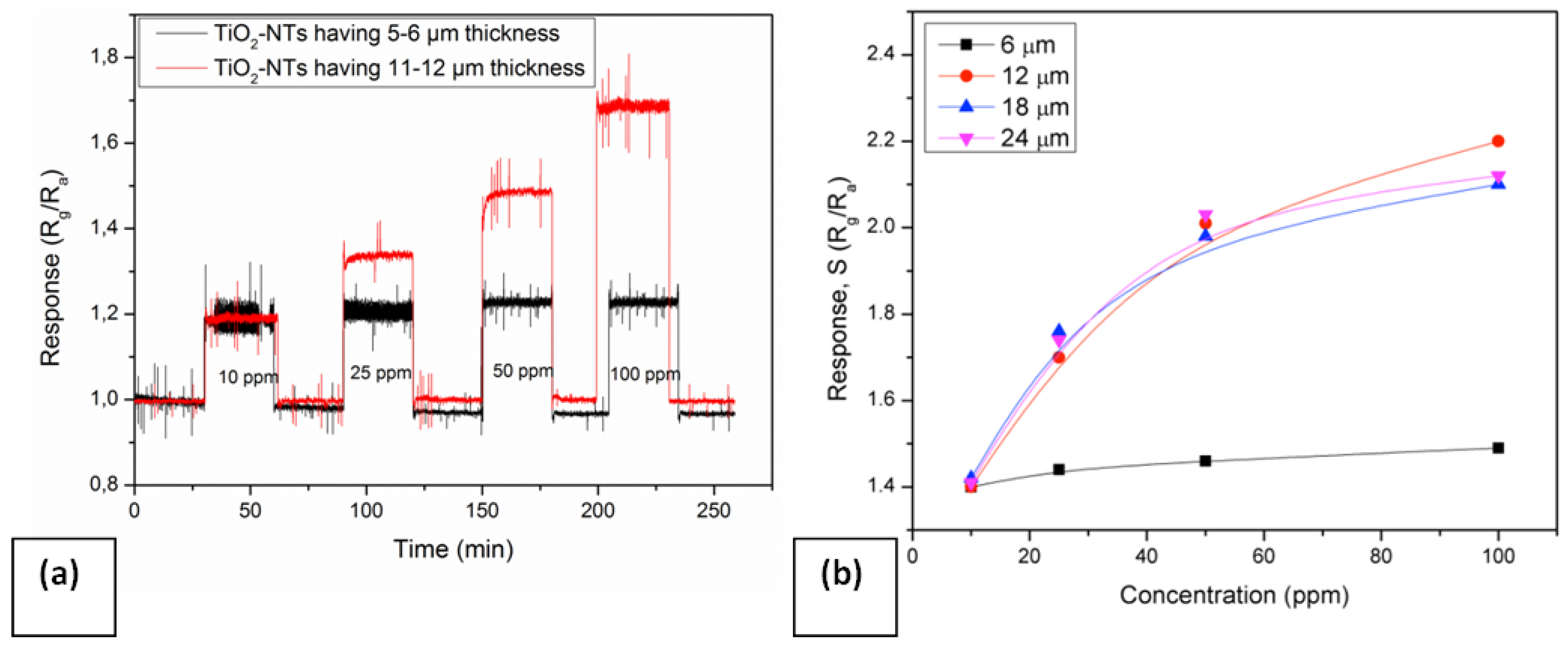
2 NTs having different thickness. The variation of sensor response with two different thicknesses of TiO2 NT layers (6 to 12 µm) are given in Figure 9a. TiO2 NTs having a thickness of 11–12 µm detect the gas concentration variation more selectively, while those of 5–6 µm thickness yield similar type of response toward all tested concentrations (i.e. 10 to 100 ppm). The sensor signals, S of the nanotubular layers with thicknesses varying from 6 to 24 µm are given in Figure 9b. The increase in the thickness of TiO2 NTs results in an improvement in the sensor response. The sensor signal, S does not vary with the amount of test gas when thinner TiO2 NTs (approx. 6 μm) are used. The thickness increase from 6 to 12 μm exhibits a higher sensitivity toward NO2 depending on the amount of testing gas. On the other hand, no more sensitivity improvement can be detected when the thickness increases above 12 μm (i.e., 18 or 24 μm). It appears that a critical thickness (dcrit.) exists at about a thickness between 6 and 12 μm. The impedance measurements support also these results. The impedance measurements of TiO2 NTs having different thicknesses have been carried out towards 25 ppm NO2 in argon ambient gas atmosphere and in pure argon atmosphere (see 
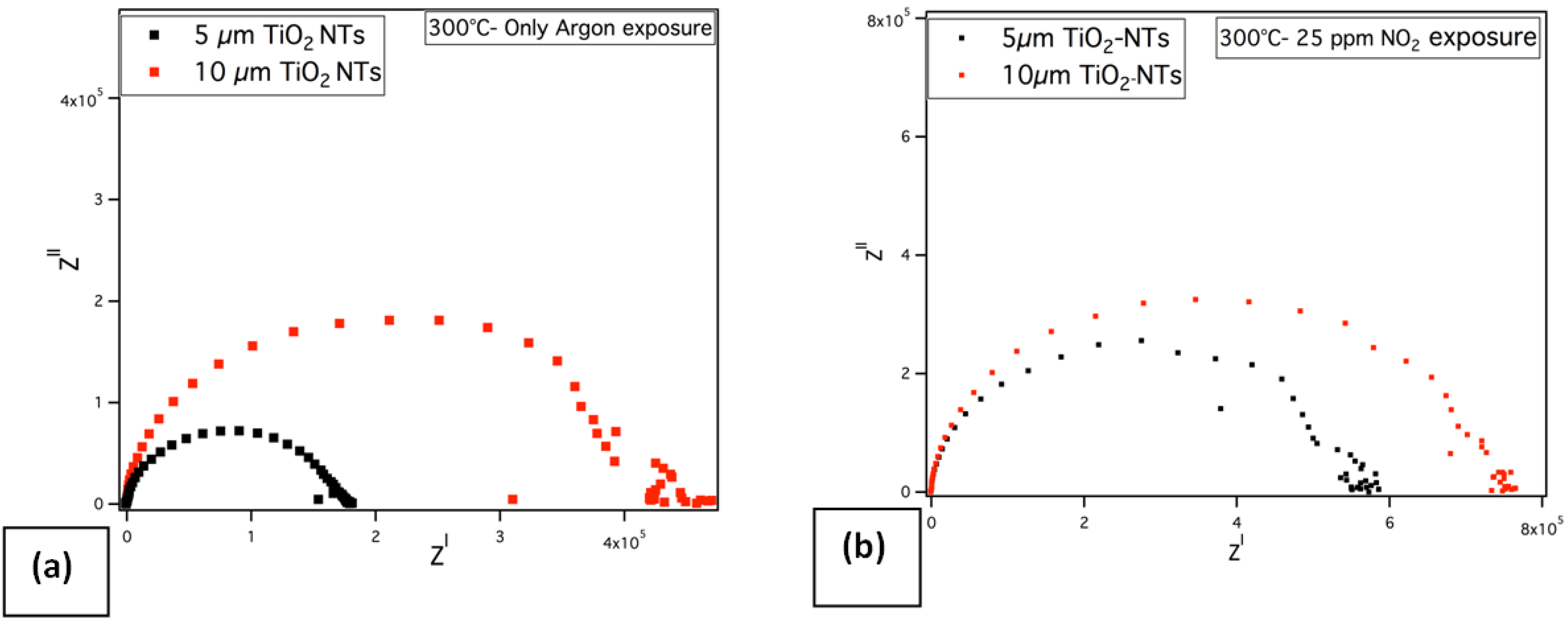
Figure 10). The impedance spectra of TiO2 NTs show solely the typical semi-circle part at high frequencies. As the thickness of TiO2 NTs increases, an increase in the complex resistance, ZI has been observed.
Figure 9. Responses of undoped TiO2 NTs for different thicknesses at 500 °C towards various NO2 concentrations (a) response versus time (b) response versus concentration.
Chemosensors 02 00069 g009
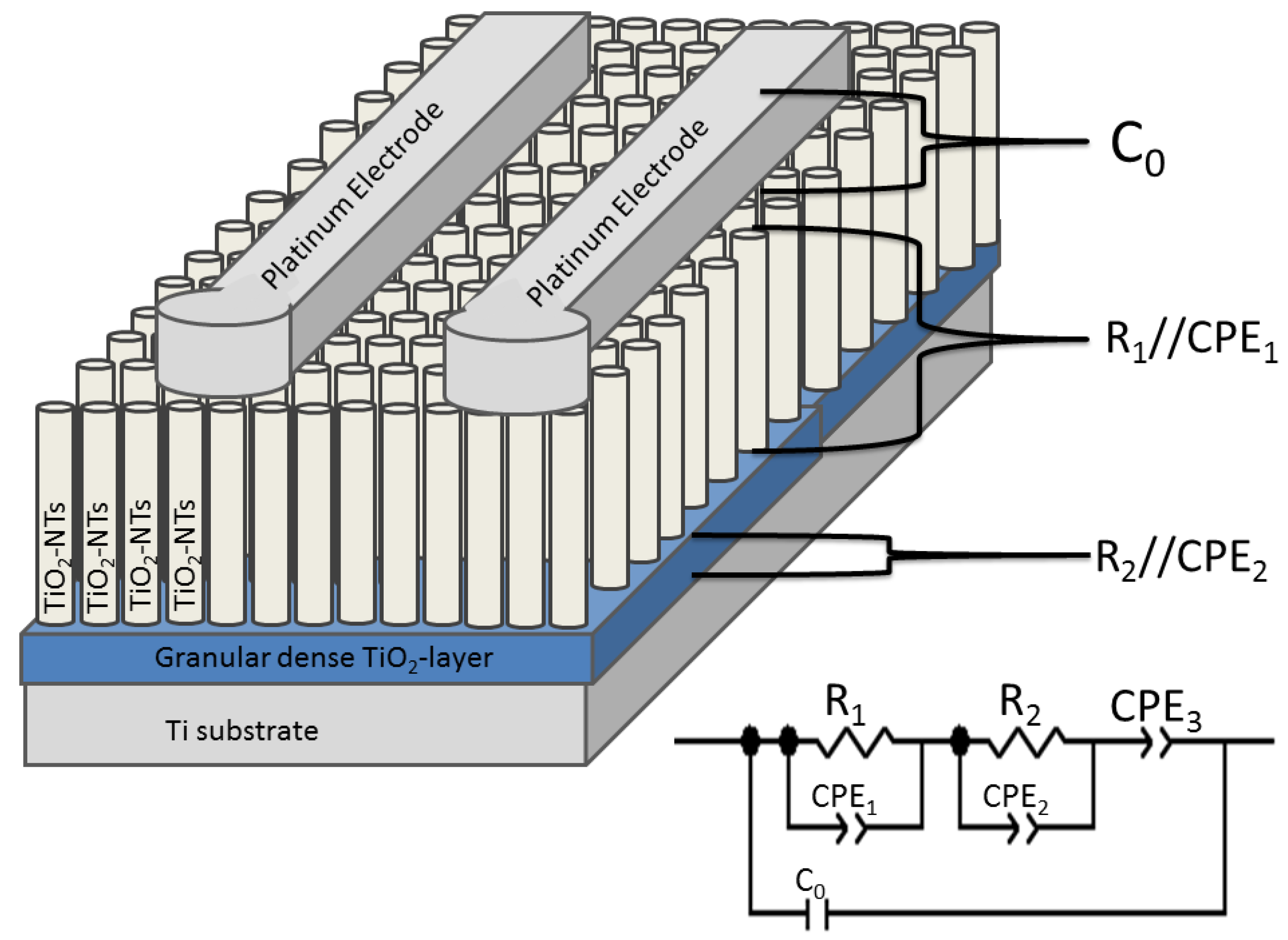
The equivalent circuit model employed in this study is given in Figure 11. According to this model, a serial connected R1||CPE1, R2||CPE2 and CPE3 was created, which was then parallel connected with a C0 representing the capacity of platinum electrodes. In the equivalent circuit model, the first compound, i.e., R1||CPE1 belongs to the TiO2 NTs, R1 representing the resistance of the TiO2 NTs. The constant phase element (CPE) is represented with the depressed semicircle in the corresponding Nyquist impedance plot as given in the literature [11] and is a calculated parameter when the circuit element is behaving in between capacitor and resistor. The constant phase element (CPE) is comprised by two components; CPE-T and CPE-P. CPE-T is a pseudo capacitance which is called Q and CPE-P is related to the semi-circle in the Nyquist plot (depressed semicircle), normally used for the notation `n`. By using CPE-P and CPE-T and resistance, one can calculate the true capacitance for the electrodes. If CPE-P equals approximately to 1, then the CPE turns theoretically to a capacitor, C [12].
The second parallel contacted elements (i.e., R2 and CPE2) belong to the dense bulk TiO2 layer present between the TiO2 NTs and Ti metal. Hereby, R2 represents the resistance of bulk TiO2 layer.
Lastly, CPE3 defines gas depended interface in order to figure out the effect of diffusion and can be regarded as the Warburg Element [12]. CPE3-T value is related to the amount of the carrier electrons on the system with a different mechanism such as diffusion [13,14,15]. Lack of diffusion in the system can cause a decrease in the CPE3-T values. It can be seen in Table 1 that CPE3-T is getting smaller with the increase of nano-tubular layer thickness and even constant above a certain thickness, indicating the reduction of diffusion above this NT thickness.
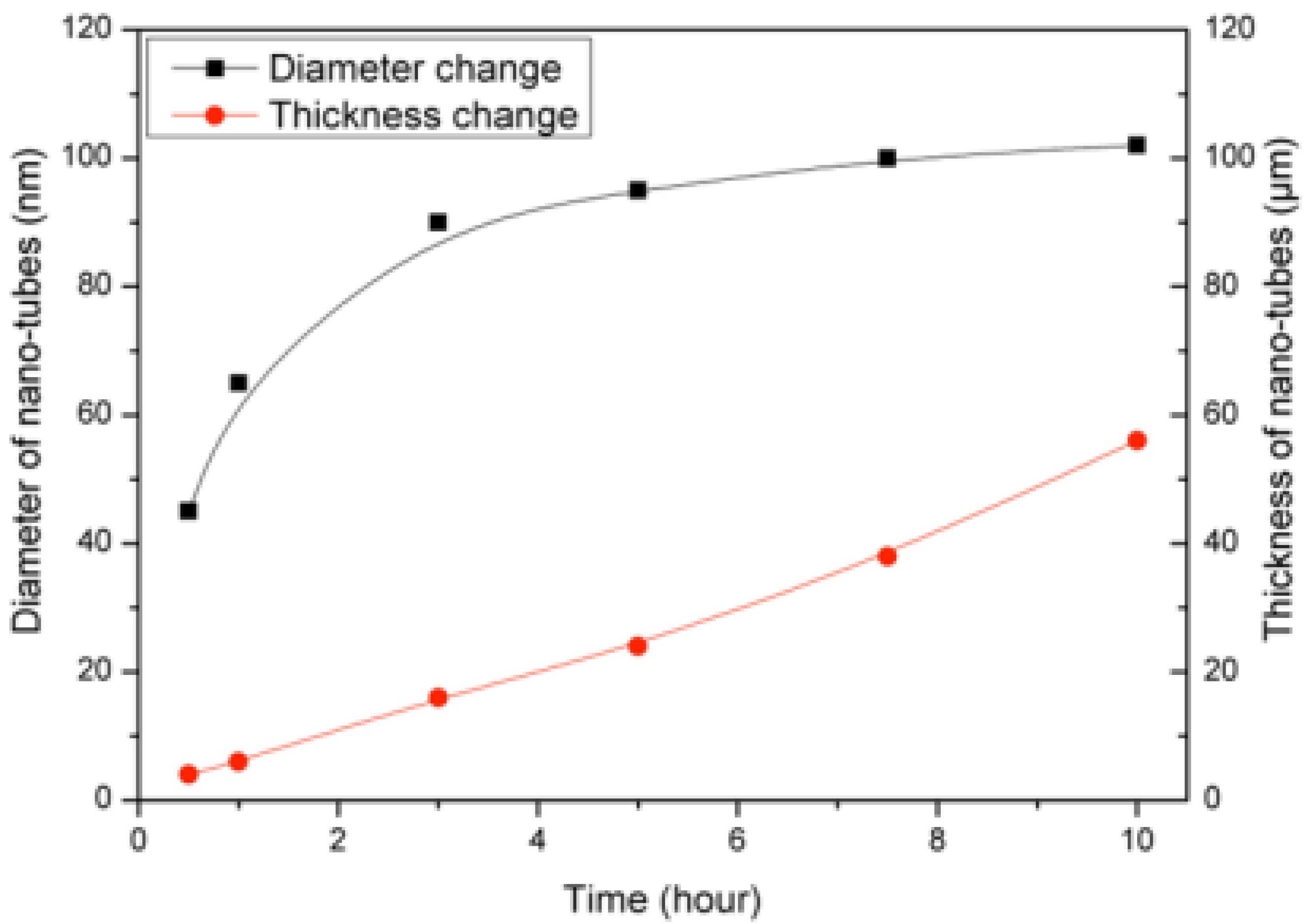
Thus, these results can be used to define the relation between sensor signal and layer thickness. On the contrary to general opinion, the present results reveal that sensor signal of TiO2 NT layers does not deteriorate on increase of layer thickness above a critical length (dcrit) despite the fact that slower gas diffusion is anticipated as the thickness of diffusion path increases. An increase in the thickness of TiO2 NTs from 12 to 24 μm resulted in a reduction of gas diffusion in the TiO2 NTs, but not in the sensitivity. At very low thickness state (e.g., 6 μm), the resistance values of the TiO2 NTs and the bulk TiO2 layer are close to each other. The electrons might have been transferred from one electrode to another electrode through both TiO2 NTs and the bulk TiO2 layer. However, after an increase in the nanotube thickness to a critical point (dcrit), the electron flow to and within the bulk TiO2 layers starts to be inhibited. Since less gas diffuses through the bottom layer of the nanotubes, less electron flow occurs in the bulk TiO2 layer. Therefore, it can be stated that the TiO2 NTs show higher resistance changes (which means higher sensitivity) as the layer thickness increases up to a critical thickness (dcrit).
Figure 10. Nyquist plots of the TiO2 NTs at different layer thickness (a) by exposing only to argon (b) towards 25 ppm NO2 in argon carrier gas at 300 °C.
Chemosensors 02 00069 g010
Figure 11. Equivalent circuit model of the sensor with TiO2 NTs indicating the corresponding sensor parts C0: capacitive, R1 and R2: resistive.
Chemosensors 02 00069 g011
Table 1. Change in resistance (R1, R2) and CPE-values of undoped TiO2 NTs layer and the bulk TiO2 depending on NTs thickness towards different amounts of NO2 at each selected measurement. Colored columns indicate the constant values, and thus reduced diffusion.
Thickness-GasR1
[Ω]
CPE1R2
[Ω]
CPE2CPE3
T
[sP/Ω]
PT
[sP/Ω]
PT
[s]
P
6 μm—Argon3.5E51E-70.91.4E53.8E-60.240.0010.1
12 μm—Argon5.2E51E-70.72.3E39E-60.51.2E-40.2
18 μm—Argon5.5E51E-70.92.4E33.8E-60.241.3E-40.1
24 μm—Argon5.6E51E-70.72.3E39E-60.51.3E-40.2
6 μm—25 ppm NO2 in Argon4.2E51.2E-80.93.3E56.6E-60.270.0040.1
12 μm—25 ppm NO2 in Argon7.2E51E-70.84.5E34.9E-70.62.1E-40.2
18 μm—25 ppm NO2 in Argon7.4E51.2E-80.93.5E36.6E-60.272.6E-40.1
24 μm—25 ppm NO2 in Argon7.2E51E-70.82.5E34.9E-70.62.6E-40.2

3.3.2. Effect of Doping on Gas Sensing Mechanism

The sensor response curves obtained with a 12 µm thick TiO2 NT layer in Figure 12 exhibit that the undoped TiO2 NT yields n-type sensor response, while the Cr doped TiO2 NT behaves as p-type semi-conductor under NO
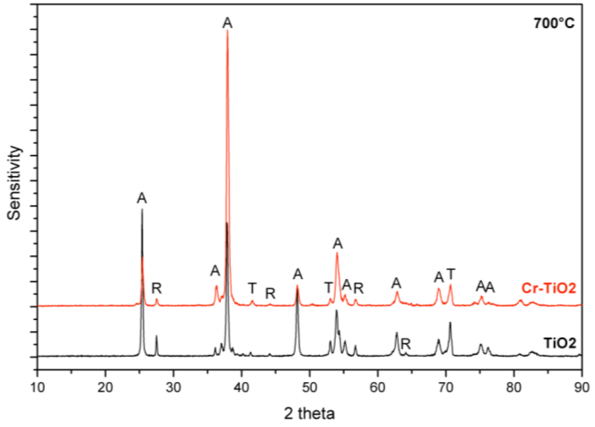
2-exposure. Considering the XRD investigation, this alteration in the sensor response type (i.e., in the semiconductor type) can be firstly attributed to the presence of rutile-phase. However, according to Savage et al., p-type semiconductor behavior can only be observed by the presence of almost pure rutile phase. After their observations, n-type semiconductor behavior is likely to be observed with a sensor layer (e.g., anatase and rutile phase mixture), which contains less than 75% rutile, being exposed to an oxidizing gas [
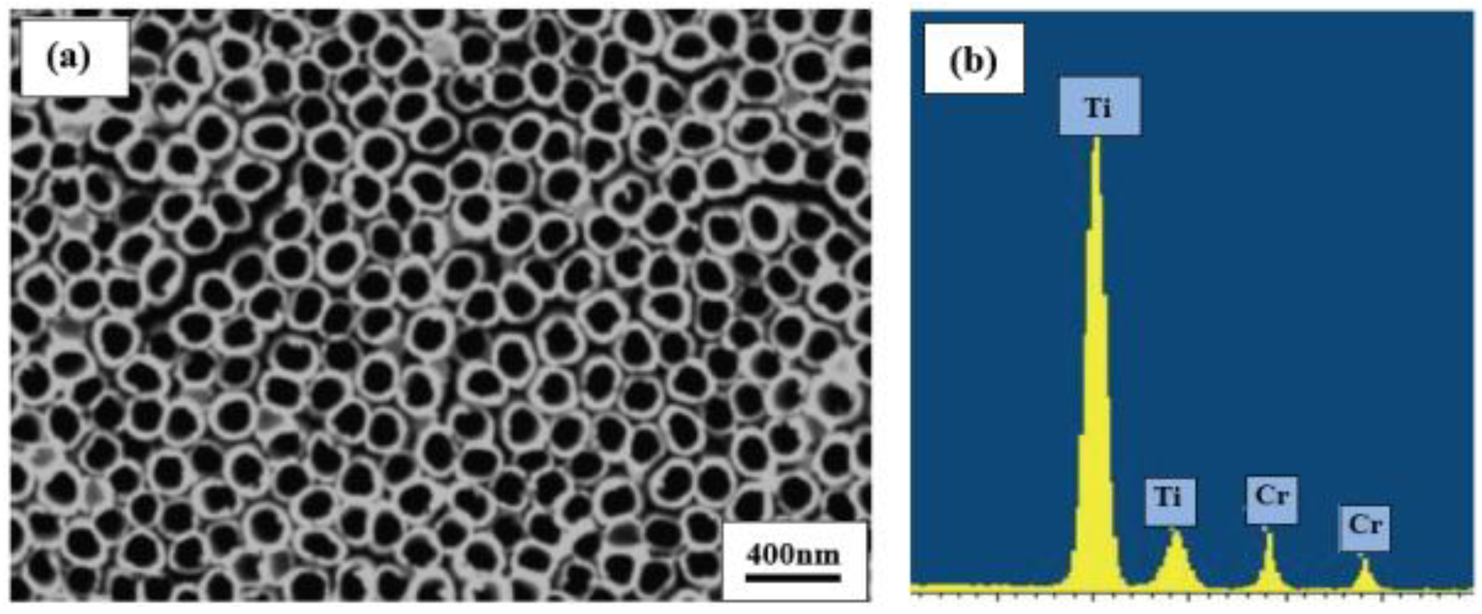
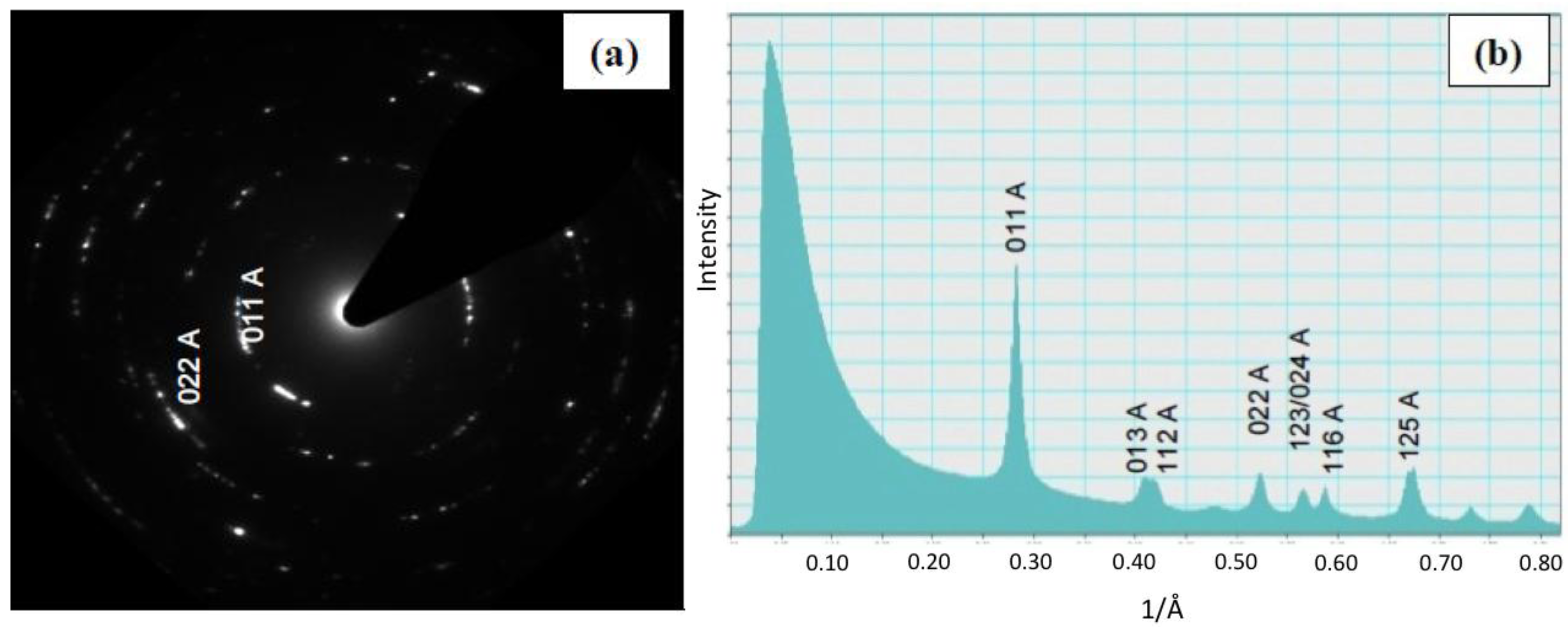
16]. Moreover, our TEM investigations showed that Cr doped TiO2 NTs which were annealed at 700 °C contain solely anatase phase. Thus, the improved sensor response of the Cr doped TiO2 NTs with p-type behavior can be attributed to the Cr3+ doping which probably induces oxygen vacancies and thus facilitates the transport of charge carriers.
Figure 12. Responses of the undoped and Cr doped TiO2–NTs sensors having a thickness of 12 µm and annealed at 700 °C towards various NO2 concentrations in argon carrier gas at 500 °C.
Chemosensors 02 00069 g012
Relying on their close ionic radius (Ti4+ in hexa-coordination is 0.745 Å; while 0.755 Å for Cr3+), it can be postulated that the incorporation of trivalent Cr3+ into the TiO2-lattice will occur without any distortion of the lattice, simply via displacement of Ti4+-sites. Upon substitution of Ti4+ by the Cr3+; the original oxygen atom of one Ti–O bond becomes electronegative resulting in a shift from its original site. Cr-substitution in Ti-sites and Oo denotes an oxygen atom at its normal lattice site, resulting in oxygen vacancies, VO. As a result of Cr doping, oxygen vacancies with a positive charge will be formed.
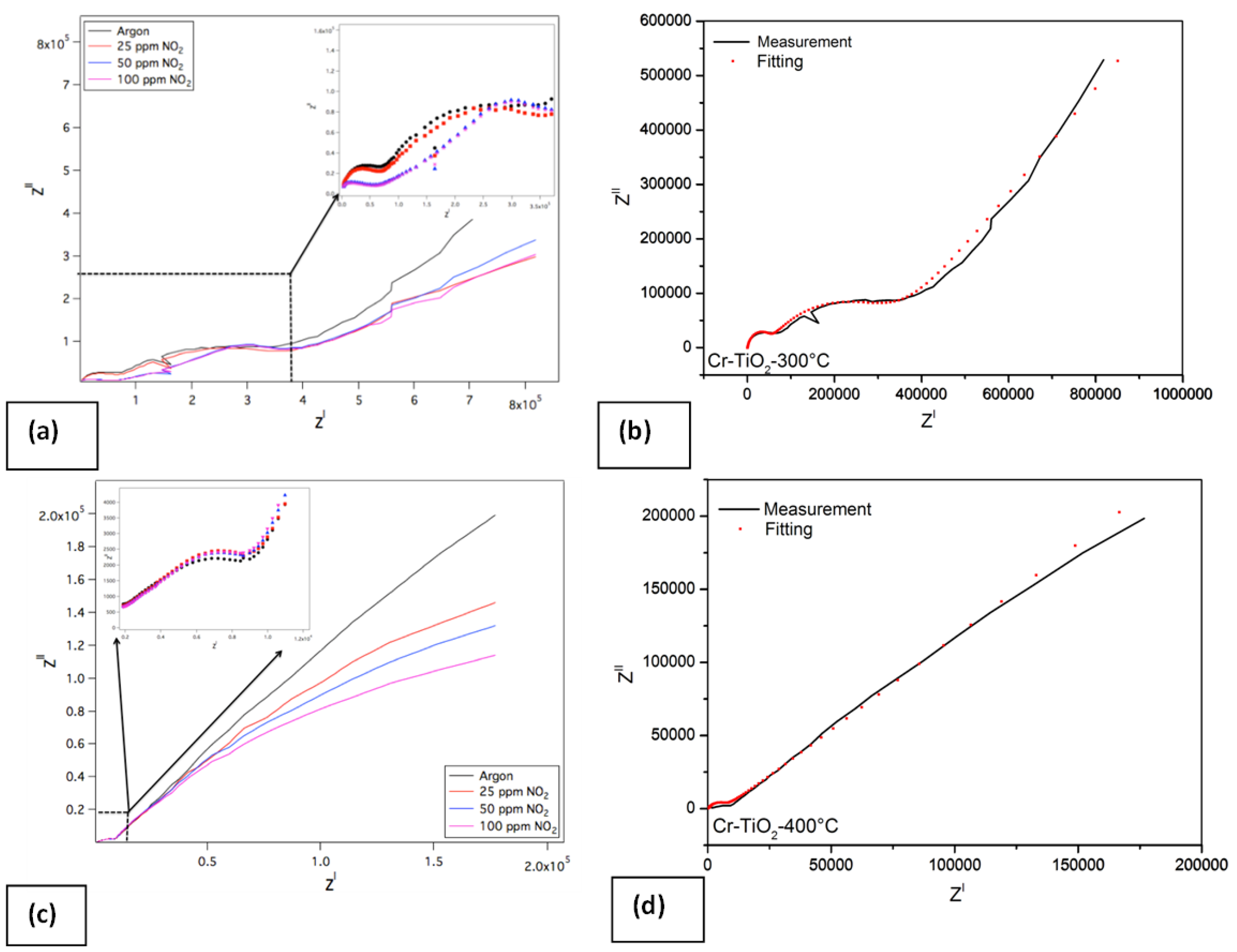
The Nyquist plot of the Cr doped TiO2 NTs for different concentrations of NO2 (25–50 and 100 ppm) at 300 °C and their fitting results are given in Figure 13. The impedance spectrum of the Cr doped TiO2 NTs differs from that of undoped TiO2 NTs, displaying two semi-circle parts. The first semi-circle is related to the grain boundary conductivity and the second one is to the bulk conductivity. Furthermore, there is one linear part that is related with the response of electrode [17]. The linear part of the impedance spectra shrinks with the NO2-concentrations rising to 25, 50 and 100 ppm respectively in argon atmosphere (see Figure 13a). The same equivalent circuit model which is given in Figure 11 is used here too in order to obtain the fitting curve. The equivalent circuit model and measurements, which were carried out at 300 °C in argon, yield a perfect fit, as can be seen in Figure 13b. The effect of temperature on sensing mechanism was also figured out and it was given in Figure 13c,d. At higher temperatures, the impedance spectra display no longer two semi-circles; instead, contains one semi-circle which is related to the grain boundary conductivity at higher frequency and one linear part at low frequencies corresponding to the diffusion of sensing gas. Nevertheless, the impedance spectra of the Cr doped TiO2 NTs yield the same behavior at 400 °C and at 300 °C. At higher concentrations of NO2, the linear part of the spectra shrinks.
Figure 13. Impedance spectra of Cr doped TiO2 NTs under different concentrations of NO2 at 300 °C (a) measurement results (b) fitting result combined with measurement and at 400 °C (c) measurements (d) fitting result combined with measurement.
Chemosensors 02 00069 g013
The numerical values of the equivalent circuit’s elements for Cr doped TiO2 NTs are given in Table 2. It is known that if CPE-P values of constant phase elements equals to approximately 1, then the CPE turns theoretically to a capacitor [13]. As it can be seen from Table 2, CPE1-P values are 1, which means CPE elements for Cr doped TiO2 NTs layers behave like capacitor at all temperature ranges. The use of this information can make an important inference for the determination of which R||CPE group represents which TiO2 layer. Above, it is described that the same element group (i.e., parallel connected R||CPE) is used to define and differentiate between two different layers, i.e., TiO2 NTs layer and dense bulk TiO2 layer lying between nanotubular layer and titanium.
Table 2. Fitting parameters of the Cr doped TiO2 NTs.
Temperature—Gas contentR1
[Ω]
CPE1R2
[Ω]
CPE2CPE3
T
[sP/Ω]
PT
[sP/Ω]
PT
[s]
P
300 °C—pure Argon43,0005.9E-91285,0009E-70,581.7E-50.5
300 °C—25 ppm NO2 in Argon40,0001.6E-81336,0001.9E-60.562.5E-50.65
300 °C—50 ppm NO2 in Argon23,0004E-91600,0002E-60.553.5E50.65
300 °C—100 ppm NO2 in Argon22,0008E-91620,0002E-60.73.8E-50.85
400 °C—pure Argon5,0003E-616,0000.0020.37.4E-50.58
400 °C—25 ppm NO2 in Argon4,1003E-616,0000.0020.36E-50.59
400 °C—50 ppm NO2 in Argon3,3003E-616,0000.0020.35.9E-50.69
400 °C—100 ppm NO2 in Argon2,9003E-616,0000.0020.35.7E-50.71
500 °C—pure Argon8005E-714500.00020.51.9E-40.5
500 °C—25 ppm NO2 in Argon7005E-714500.00020.51.7E-40.51
500 °C—50 ppm NO2 in Argon4505E-714500.00020.51.6E-40.51
500 °C—100 ppm NO2 in Argon4005E-714500.00020.51.6E-40.54
The resistance values of the first compound R1, which represents the TiO2 NTs, decreases as the amount of the test gas NO2 concentration increases. On the other hand, the resistance values of the second compound R2, which represents bulk TiO2 layer, increases with increasing NO
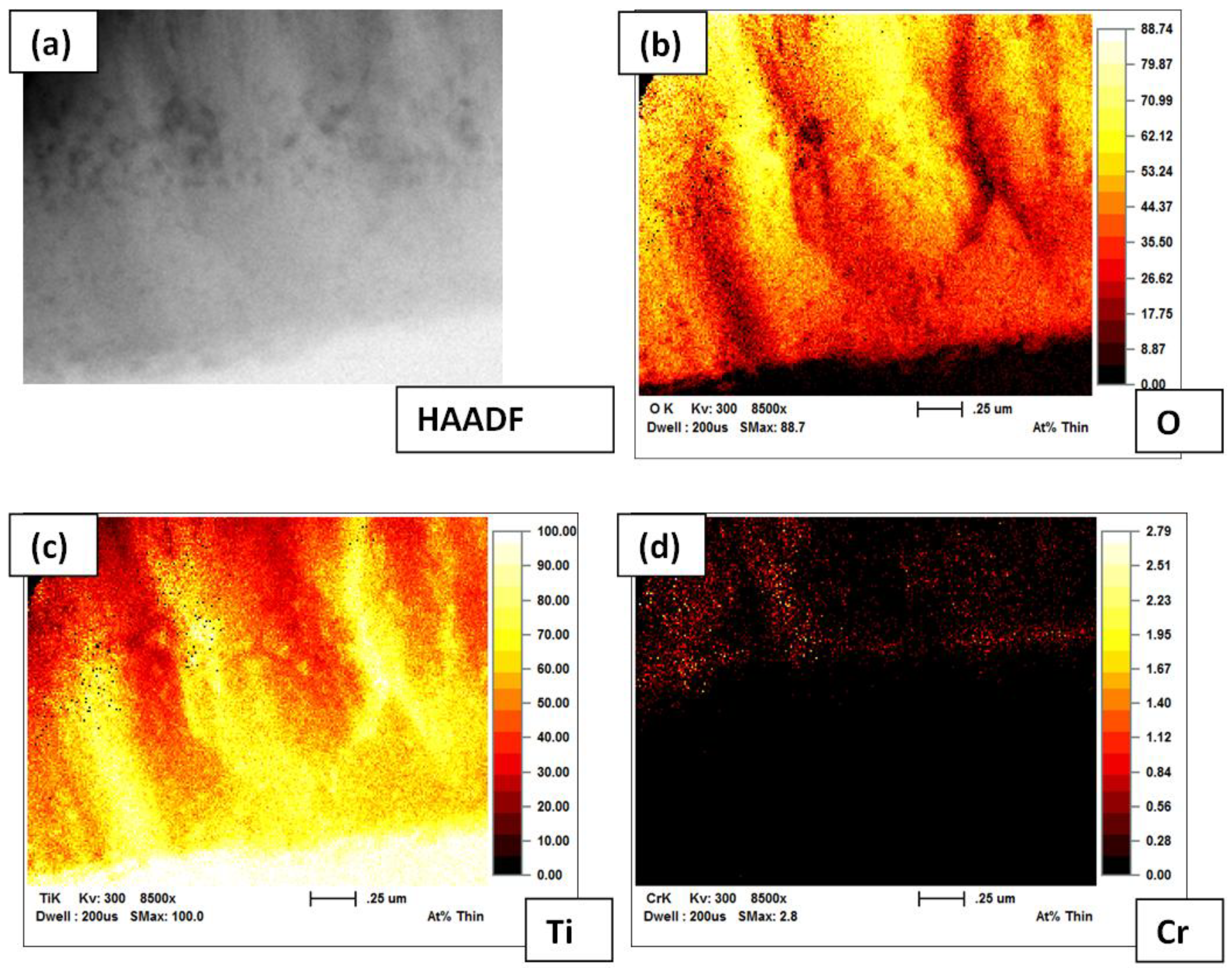
2 amount. As explained previously, a decrease in resistance towards oxidizing gases is a typical behavior for p-type semi-conductive metal-oxides; while an increase in the resistance for n- type semi-conductive metal-oxide is expected. TEM investigations and EDX-mapping results showed that Cr is situated only inside the TiO2 NTs, while no presence of Cr was detected by TEM in the bulk TiO2 layer which lies beneath the nanotubular TiO2 (see Figure 6). As a result, while Cr doped TiO2 NTs exhibits p-type sensor behavior, the bulk TiO2 layer contributes to the behavior of n-type semiconductor. After all, the different responses at R1 and R2 values towards NO2 support this idea correlating the relation between the different circuit elements with the different morphological parts of TiO2.
Impedance spectra show a reduction at the linear part of the graph (i.e., low frequency part) with the increase of test-gas concentrations. At equivalent circuit model, the linear part of the spectra is found to depend on the value of CPE3, which is responsible for the gas related interface. It is known that the CPE-T value varies mostly with the amount of the transported electrons at the system. Increasing the amount of NO2 in the system causes more reactions on the walls of the TiO2 NTs. This means that the more reactions occur on the wall surface, the more electrons are transported within the system. Thus, the observed increase in the value of CPE3-T is plausible and this causes a lowering at the linear part of the impedance spectra as the amount of the test gas increases.
Temperature dependent change in resistance for semiconductors is given with the Equation (1):
Chemosensors 02 00069 i001
The applied sensor behaves as a chemo-resistive system therefore the Equation (2) which applies generally for resistors is used for TCR (Temperature Coefficient of Resistance) calculations [18].
R(T) = R0[1 + α(TT0)]
where R0 is the resistance at the temperature T
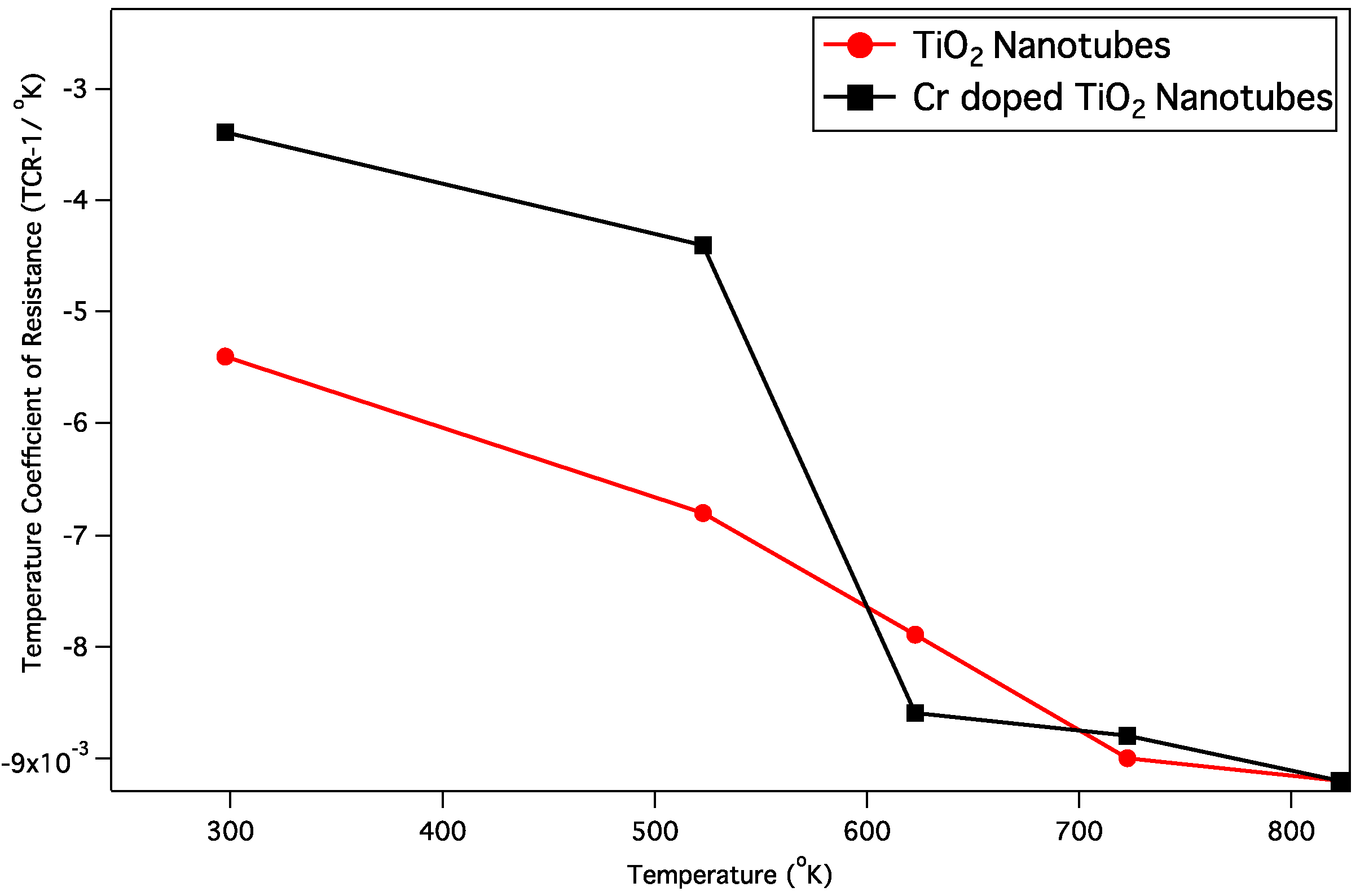
0 and α is the temperature coefficient of resistance (TCR) which is usually positive for metals at room temperature and negative for semiconductors and insulators. By applying this equation, easier experimental measurement is possible to demonstrate that the employed NTs exhibit negative TCR values. As Figure 14 shows, both TiO2 NTs samples (undoped and Cr doped) have negative TCR-values, which means that the temperature increase causes a decrease in the surface resistance of semi-conductive nanotubular layer.
Figure 14. Temperature coefficient of resistance (TCR) values of the undoped and Cr doped TiO2 NTs depending on different temperatures.
Chemosensors 02 00069 g014
The used equivalent circuit parameters showed that the increase of the temperature causes a decrease in both resistance values, R1 and R2, as expected. The resistance of the Cr doped TiO2 NTs which is represented by R1 decreases also depending on NO2 concentration at higher concentrations. On the other hand, the resistance of the bulk TiO2 layer towards test gas, NO2 changes only at lower temperature (below 400 °C). Above 400 °C, the bulk TiO2 layer shows no response to the NO2 concentration changes. At the temperatures above 400 °C, the bulk conductivity of bulk TiO2 becomes less effective as the grain boundary of the nano-tubes becomes more dominant. In addition, CPE2-T value of the bulk TiO2 layer remains stable even at higher NO2 concentrations. The constant CPE2-T rate is a sign of constant electron transfer in the bulk TiO2 layer. It is already reported in the literature that the grain boundary conductivity increases with the increase of temperature [19,20,21]. As indicated in the literature as well as the obtained impedance results show, the grain boundary conductivity of the Cr doped TiO2 NTs became more dominant than the conductivity of thin bulk TiO2 layer as temperature increases from 300 °C to 400 °C. In other words, increased grain boundary conductivity achieved by Cr doping provides an easy pathway for electron transfer eliminating the role of denser thin bulk TiO2-layer beneath the TiO2 NTs. Thus, it can be attributed that the doped transient oxides (e.g., TiO2-NTs) may lead to higher sensitivity in gas sensors. However, no further influence of grain boundary or bulk conductivity can be anticipated for the sensors selectivity [22]. It is more likely that selectivity of a sensor layer will relate to the band gap structure of the sensing material.

4. Conclusions

In this work the focus has been given onto the understanding the mechanism of the TiO2 NTs and doping effect on sensing behavior using the equivalent circuit model of impedance response towards NO2.Vertically aligned TiO2 NTs were synthetized through the anodization process in an EG-based solution. Cr doping into TiO2 NTs process was achieved by employing a simple but effective chemical route. Both un-doped and Cr doped TiO2 NTs yield a stable response towards NO2 at test temperatures as high as 500 °C. The impedance measurements show that the sensing mechanism develops in dependency of TiO2 NTs thickness, temperature or dopant elements. The thickness of the nano-tubular layer has an influence on sensing mechanism until a certain thickness (dcrit.) is reached. However, after this critical point, the thickness does not affect the sensing properties. This situation can probably be related to the lack of diffusion. The grain boundary and bulk conductivity appear to be the main control mechanisms of sensing in these layers. The grain boundary conductivity is mostly related to the conductivity of the nano-tubular part of the sensor, and the bulk conductivity is related with the dense oxide layer, which is present beneath the nano-tubular oxide layer. It is observed that the grain boundary conductivity could be increased either by increasing the temperature or doping into the TiO2 NTs.

Conflicts of Interest

The authors declare no conflict of interest.

References

  1. Yamazoe, N. New approaches for improving semiconductor gas sensors. Sens. Actuators B 1991, 5, 7–19. [Google Scholar] [CrossRef]
  2. Kim, I.-D.; Rothschild, A.; Tuller, H. Advances and new directions in gas-sensing devices. Acta Met. 2013, 61, 974–1000. [Google Scholar] [CrossRef]
  3. Şennik, E.; Çolak, Z.; Kılınç, N.; Öztürk, Z.Z. Synthesis of highly-ordered TiO2 nanotubes for a hydrogen sensor. Int. J. Hyd. Energy 2010, 35, 4420–4427. [Google Scholar] [CrossRef]
  4. Comini, E.; Sberveglier, G. Metal oxide nanowires as chemical sensors. Mater. Today 2010, 13, 36–44. [Google Scholar] [CrossRef]
  5. Gönüllü, Y.; Mondragón, G.M.R.; Saruhan, B.; Ürgen, M. Improvement of gas sensing performance of TiO2 towards NO2 by nano-tubular structuring. Sens. Actuators B 2012, 169, 151–160. [Google Scholar] [CrossRef]
  6. Jun, T.H.; Lee, K.S. Cr-doped TiO2 thin films deposited by RF-sputtering. Mater. Lett. 2010, 64, 2287–2289. [Google Scholar] [CrossRef]
  7. Choia, Y.; Seeleya, Z.; Bandyopadhyaya, A.; Bosea, S.; Akbar, S.A. Aluminum-doped TiO2 nano-powders for gas sensors. Sens. Actuoators B 2007, 124, 111–117. [Google Scholar] [CrossRef]
  8. Coa, C.; Li, J.; Wang, X.; Song, X.; Sun, Z. Current characterisation and growth mechanism of anodic titania nanotube arrays. J. Mater. Res. 2011, 26, 437–442. [Google Scholar] [CrossRef]
  9. Liu, S.-Y.; Tang, Q.-L.; Feng, Q.-G. Synthesis of S/Cr doped mesoporous TiO2 with high-active visible light degradation property via solid state reaction route. Appl. Surf. Sci. 2011, 257, 5544–5551. [Google Scholar] [CrossRef]
  10. Ghicov, A.; Schmidt, B.; Kunze, J.; Schmuki, P. Photoresponse in the visible range from Cr doped TiO2 nanotubes. Chem. Phys. Lett. 2007, 433, 323–326. [Google Scholar] [CrossRef]
  11. Wang, M.; Wang, L.; Wang, G.; Ji, X.; Bai, Y.; Li, T.; Gong, S.; Li, J. Application of impedance spectroscopy for monitoring colloid Au-enhanced antibody immobilization and antibody–antigen reactions. Biosens. Bioelectron. 2004, 19, 575–582. [Google Scholar] [CrossRef]
  12. Carrara, S.; Bavastrello, V.; Ricci, D.; Stura, E.; Nicolini, C. Improved nanocomposite materials for biosensor applications investigated by electrochemical impedance spectroscopy. Sens. Actuators B 2005, 109, 221–226. [Google Scholar] [CrossRef]
  13. Hagen, G.; Dubbe, A.; Rettig, F.; Jerger, A.; Birkhofer, T.; Müller, R.; Plog, C.; Moos, R. Selective impedance based gas sensors for hydrocarbons using ZSM-5 zeolite films with chromium(III) oxide interface. Sens. Actuators B 2006, 119, 441–448. [Google Scholar] [CrossRef]
  14. Bisquert, J.; Garcia-Belmonte, G.; Bueno, P.; Longo, E.; Bulhoes, L.O.S. Impedance of constant phase element (CPE)-blocked diffusion in film electrodes. J. Electroanal. Chem. 1998, 452, 229–234. [Google Scholar] [CrossRef]
  15. Bisquert, J.; Belmonte, G.G.; Fabregat-Santiago, F.; Bueno, P.R. Theoretical models for ac impedance of finite diffusion layers exhibiting low frequency dispersion. J. Electroanal. Chem. 1999, 475, 152–165. [Google Scholar] [CrossRef]
  16. Savage, N.O.; Akbar, S.A.; Dutta, P.K. Titanium dioxide based high temperature carbon monoxide selective sensor. Sens. Actuators B 2001, 72, 239–248. [Google Scholar] [CrossRef]
  17. Ward, M.R. Electrical Engineering Science; McGraw-Hill Book Co.: New York City, NY, USA, 1971; pp. 36–40. [Google Scholar]
  18. Avila-Paredes, H.; Choi, K.; Chen, C.T.; Kim, S. Dopant-concentration dependence of grain-boundary conductivity in ceria: A space-charge analysis. J. Mater. Chem. 2009, 19, 4837–4842. [Google Scholar] [CrossRef]
  19. Guo, X.; Ding, Y. Grain boundary space charge effect in zirconia. J. Electrochem. Soc. 2004, 151, J1–J7. [Google Scholar] [CrossRef]
  20. Hagenbeck, R.; Waser, R. Influence of temperature and interface charge on the grainboundary conductivity in acceptor-doped SrTiO3 ceramics. J. Appl. Phys. 1998, 83, 2083–2092. [Google Scholar] [CrossRef]
  21. Martin, M. Grain boundary ionic conductivity of yttrium stabilized zirconia as a function of silica content and grain size. Solid State Ionics 2003, 161, 67–79. [Google Scholar] [CrossRef]
  22. Kosacki, I.; Anderson, H.U. Nanostructured oxide thin films for gas sensors. Sens. Actuators B 1998, 48, 263–269. [Google Scholar] [CrossRef]

