
Two-Dimensional Transition Metal Disulfides for Chemoresistive Gas Sensing: Perspective and Challenges


1
Department of Materials Science and Engineering, Research Institute of Advanced Materials, Seoul National University, Seoul 08826, Korea
2
School of Chemical Engineering and Materials Science, Chung-Ang University, Seoul 06974, Korea
*
Author to whom correspondence should be addressed.
Chemosensors 2017, 5(2), 15; https://doi.org/10.3390/chemosensors5020015
Submission received: 5 April 2017
/
Revised: 1 May 2017
/
Accepted: 3 May 2017
/
Published: 5 May 2017
(This article belongs to the Special Issue Novel 2D-Inorganic Materials for Gas Sensing)
Abstract
:Transition metal disulfides have been attracting significant attentions in recent years. There are extensive applications of transition metal disulfides, especially on gas sensing applications, due to their large specific surface-to-volume ratios, high sensitivity to adsorption of gas molecules and tunable surface functionality depending on the decoration species or functional groups. However, there are several drawbacks such as poor gas selectivity, sluggish recovery characteristics and difficulty in the fabrication of large-scale devices. Here, we provide a review of recent progress on the chemoresistive gas sensing properties of two-dimensional transition metal disulfides. This review also provides various methods to enhance the gas sensing performance of two-dimensional disulfides, such as surface functionalization, decoration receptor functions and developing nanostructures.
1. Introduction
The Internet of Things (IoT), which is frequently mentioned along with “connected devices” and “smart devices”, is the inter-networking of vehicles, buildings, physical devices and other items, which include the electronics, actuators, sensors software and network connectivity that enable these objects to collect and exchange data [1]. One of the key components enabling the IoT is sensors, as they provide enormous information by sensing things and monitoring the environment. Gas sensors are devices or instruments that produce a measurable signal output in order to determine the detectable presence, concentration or quantity of a particular target chemical substance (analyte) present in gas. Such gas sensors are necessary for various applications of IoT, including building automation, healthcare and life sciences, consumer and home automation, transportation, industrial, environment, security and public safety and retail and logistics. Gas sensors for use in the IoT should possess basic performance, like high sensitivity, good selectivity and stability, and meet special requirements, such as low cost, low power consumption, small size and easy integration into existing technologies [2].
Among various types of gas sensors, chemoresistive gas sensors based on semiconductors have been considered as suitable candidates for the IoT due to low cost and small size [3]. Gas sensors based on nanostructured semiconducting metal oxides (typically spherical nanoparticles) lead to high responses to various gases [4,5,6,7]. They should operate at elevated temperatures with external heaters in order to keep the materials sensitive to the target analytes. However, the use of an external heater not only increases the power consumption of the sensor, but also causes thermal stability problems, obstructing practical applications for the IoT [2]. To overcome the intrinsic problems of semiconducting metal oxides for chemoresistive gas sensors, two-dimensional (2D) materials, including graphene, reduced graphene oxide and MoS2, have attracted remarkable interest for their potential as active materials for gas sensors [8,9,10,11]. Due to the high surface-to-volume ratios and easiness in device fabrication, the application of many 2D materials was made on gas sensing in their early development stage. While graphene is metallic with zero band gap energy, many transition metal disulfides, such as MoS2, WS2 and SnS2, are semiconducting with tunable bandgap energies depending on the thickness [12]. In this respect, the transition metal disulfides are inherently more desirable than graphene for chemoresistive gas sensing applications.
In this review, gas sensors based on 2D transition metal disulfides are introduced thoroughly with strong emphasis on the sensing material and underlying gas sensing mechanism. While the gas sensors based on individual 2D transition metal disulfides are successfully demonstrated for fundamental research, obstacles for practical applicability are discussed to mention challenges to be addressed for commercializing 2D transition metal disulfide gas sensors. Some crucial issues including long-term stability, selectivity of the sensors and array fabrication are discussed.
2. Gas Sensors Based on Transition Metal Disulfides
2.1. General
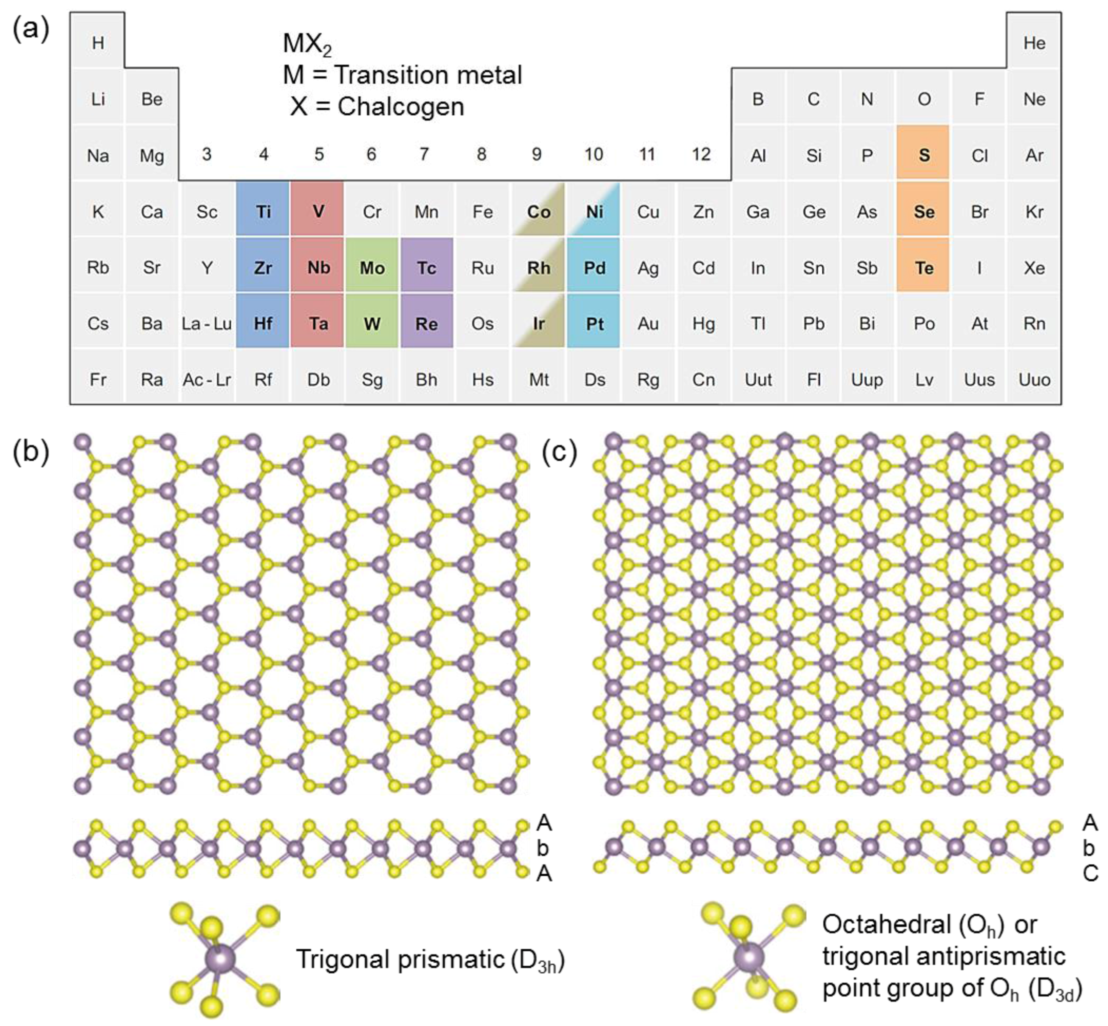
Bulk transition metal dichalcogenides, MX2, have layered structures of X-M-X, where M represents a layer of transition metal atoms, which is hexagonally packed and sandwiched between two X, which represent chalcogen atoms. In general, the thickness of each layer is about 6–7 Å [13]. About 40 different layered transition metal dichalcogenide compounds exist, as shown in Figure 1a [12]. The highlighted elements in the periodic table present the transition metals and the three chalcogen elements (S, Se and Te), which have a predominant tendency to crystallize in X-M-X layered structures. Co, Rh, Ir and Ni are partially highlighted, which present that only a portion of the dichalcogenides has layered structures. For instance, NiTe2 is reported to have a layered compound, while NiS2 shows a pyrite structure. The layers are connected by weak van der Waals forces as the M-X bonds within layers are typically covalent. This results in the easy splitting of the crystal along the layer boundaries. Four electrons donated from the metal fill the bonding state of a transition metal dichalcogenide. Therefore, the metal and sulfur atoms have +4 and −2 of the oxidation states, respectively. The lone pair electrons of the sulfur atoms are placed at the end of the layer surfaces, and the layers have been stable against the interaction between environmental species with the absence of dangling bonds. The metal of layered transition metal dichalcogenides can have the coordination either in the trigonal prismatic structure or the octahedral structure, determined by the arrangement of the metal and chalcogen elements (Figure 1b,c). Several polymorphs can be adopted to the transition metal dichalcogenides by the type of layer stacking orders. Trigonal, hexagonal and rhombohedral are the most common polymorphs, which can be represented by 1T, 2H and 3R, while the numbers represent the number of X-T-X units in the unit cell, in other words, the number of layers in the stacking sequence. Some transition metal dichalcogenides can be formed in several polymorphs and stacking sequences. For instance, the 2H phase is the most common polymorph of MoS2 in nature, as it is the most stable form, while the 3R phase is often adopted to the synthetic MoS2 to form a stacking sequence of AbA BaB and AbA CaC BcB, respectively, if we symbolize the chalcogen atom layers by capital letters and the metal atom layers by lower-case letters. TiS2 is largely formed in the 1T phase and the stacking sequence of AcB.
Among the three chalcogen elements, sulfur is the most favorable atom since it is the most Earth-abundant among them and most of the MS2 (transition metal disulfide) compounds are less toxic and more stable in air than MSe2 and MTe2. Figure 2a shows the number of publications on gas sensors based on transition metal disulfides since 2011. The number of publications is rapidly increasing, and it is expected that the number will be over 100 this year. MoS2 is one of the most noted transition metal disulfide materials studied in gas sensing applications, as shown in Figure 2b. Seventy-five percent of publications up to now were focused on MoS2 along with WS2 (14%), SnS2 (9%), etc. The predominance of MoS2 over other transition metal disulfides is due to the fact that the material is the easiest material to synthesize and the most stable.
2.2. Molybdenum Disulfide
MoS2 is one of the most notable transition metal disulfides, which is a layered compound, similar to graphite. Each layer is composed of a plane of Mo atoms sandwiched between planes of S atoms. Compared with graphite and graphene, the MoS2 semiconductor has an indirect bandgap (~1.2 eV). It also has catalytic properties, which are effective for hydrodesulfurization [14]. Several works that have been reported recently have shown that an indirect band gap, a property of bulk MoS2 semiconductor, can be modified by making a single monolayer of MoS2: it converts from an indirect band gap to a direct band gap semiconductor (~1.9 eV) with superior luminescence efficiency [15,16]. It also can be applied for the transport channel of a field effect transistor (FET) with an excellent on/off ratio [17] and noticeable photoresponse [18,19].
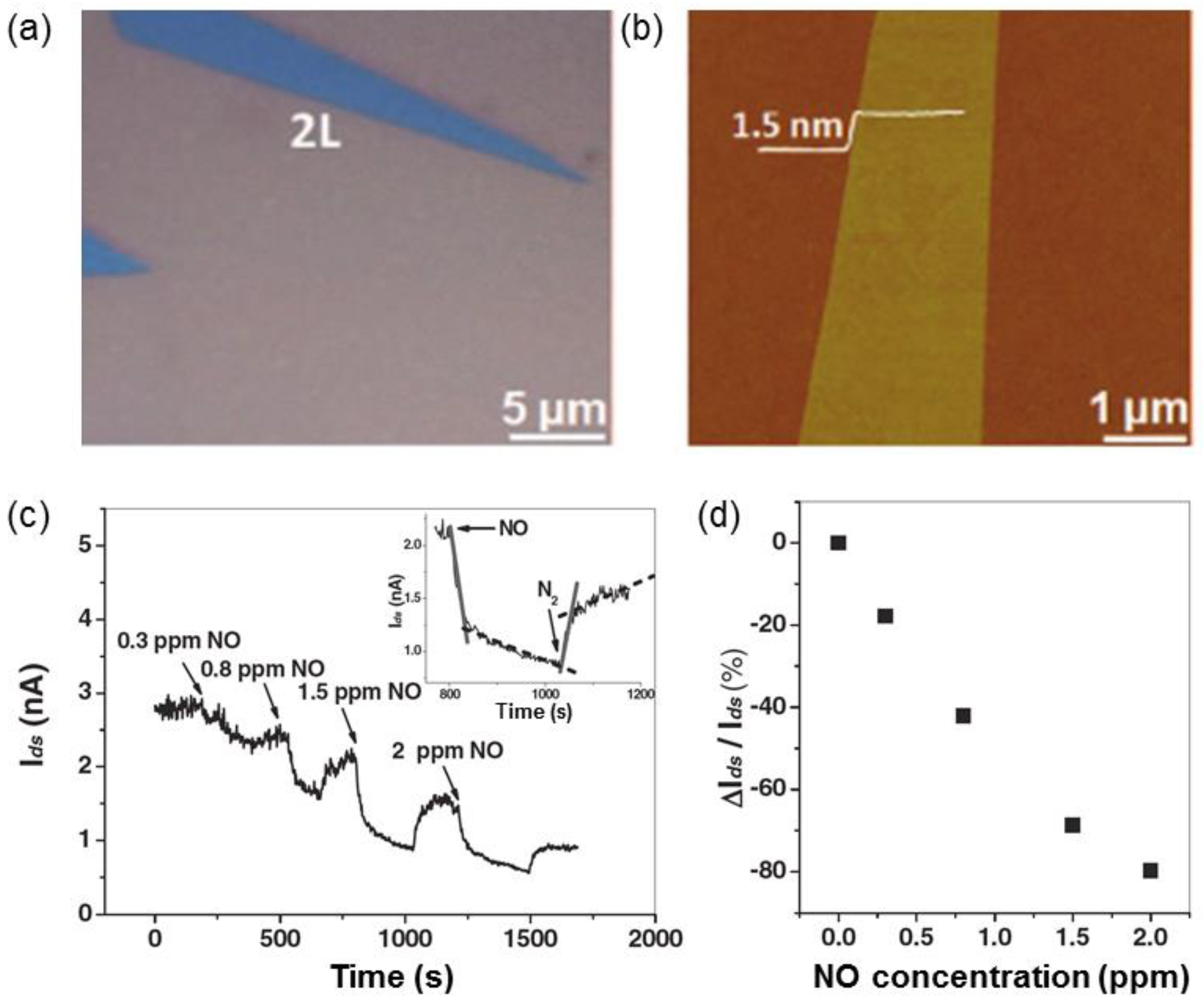
Li et al. demonstrated the gas sensing ability of FET based on a single- and multi-layer MoS2 films deposited onto 300 nm-thick SiO2 layer/Si substrates [20]. Single- and multi-layer MoS2 nanosheets are fabricated by the mechanical exfoliation technique (Figure 3a,b) [17,21,22]. The prepared MoS2 FET devices have an n-type semiconductor behavior. The current on/off ratio of bilayer (2L), trilayer (3L) and quadrilayer (4L) MoS2 devices is higher than 103 (Vg from −10–10 V), while the single-layer (1L) MoS2 FET has smaller values (≈ 102). The prepared single- and multi-layer MoS2 FETs are measured with NO gas at room temperature. The results show that the FET sensors fabricated with 2L, 3L and 4L MoS2 films have a pronounced sensitivity to NO and that the detection limit is 0.8 ppm (parts-per-million). By comparison, the monolayer MoS2 device exhibits a rapid, but unstable response. Figure 3c shows a typical current response of a 2L MoS2 FET device during the exposure to NO with a concentration range from 0.3 to 2 ppm. The p-doping effect contributes to the decrease of the current, which means the increase of the resistance during the exposure to NO [8,10,11,23]. It is similar to the charge transfer mechanism that occurs in the gas sensors based on 2D graphene [24] and 1D carbon nanotube [25]. The desorption and adsorption processes of NO can be split into two steps; one is a rapid and the other is a slow process. This phenomenon also can be found in the gas sensors based on graphene and explained by the different binding energies originating from each interaction between gas molecules and the different defect sites on the surface of the sensing materials [10].
Perkins et al. reported that single monolayer MoS2 operates with high performance as a chemical sensor at room temperature, showing high selectivity to various analytes [26]. They produced sensors with planar structures composed with a monolayer MoS2 channel on SiO2/Si substrates, as shown in Figure 4a,b. The sensor with the MoS2 monolayer shows a distinct response to triethylamine (TEA-N(CH2CH3)3) exposure, which is a laboratory-safe decomposition product from the V series nerve gas agents. The degree of the conductivity variation rises as the TEA concentration increases. The response of the device to a sequence of pulses is shown in Figure 4d. Over the sequence of pulses, the TEA concentration increases from 0.002% P0 (1 ppm) to 0.2% P0 (100 ppm) in 450 s. The response of the device to a sequence of acetone (CH3)2CO pulses is shown in Figure 4e. The acetone concentration increases from 0.02% P0 (50 ppm) to 2% P0 (5000 ppm). The incremental trend of conductivity is highly correlated with the sequence of exposure pulses, while the amplitude of ΔG/G0 is on a par with a given concentration. Compare to the relatively high responses to the exposure of the TEA and the acetone, the MoS2 sensor shows almost no variation in conductivity to the exposure of analytes that are considered to be electron acceptors or weak donors. For instance, Figure 4f shows the response to a sequence of nitrotoluene (NT) pulses, a laboratory-safe simulant for the explosive trinitrotoluene (TNT). The MoS2 monolayer exhibits no variation in conductivity as the NT concentration increases from 0.01% P0–1% P0. For the sake of contrast, the response of the CNT network sensor is presented. The conductivity of the CNT increases significantly to the exposure. They hypothesized that the interaction mechanism between the analyte and the device is regulated by the localized lone pair orbitals of the sulfur end units. The Mo 3dyz orbitals and S 2p orbitals are placed on the surface plane as the charge density distributions make the Mo 3dyz slightly reduced (negatively charged) and the S 2p slightly oxidized (positively charged) [12]. Therefore, they can easily interact with the target analytes. They suspected that the SiO2 substrate under the MoS2 monolayer has its own positive charge; therefore, the negative charge of the Mo 3dyz orbitals can be compensated. As a result, the positively-charged S is only available for the interaction between the gas molecules and the surface. Hence, the MoS2 sheet has a significant interaction with donor-like analytes, corresponding to the experimental results.
Late et al. reported the sensing performance of a MoS2 thin-layered structure transistor to the exposure of NO2 and NH3 in several conditions such as gate bias at room temperature [27]. As shown in Figure 5a, the electron-beam lithography is used for patterning Ti/Au electrodes on top of isolated MoS2 sheets, and the back gate geometry is also used for the fabrication of the gas-sensing devices. The single-layer MoS2 device shows unstable current variation over time as presented earlier [20], while multilayer MoS2 devices show better stable responses. They measured sensing behavior with and without applying back gate voltage (+15 V) for two-layer and five-layer MoS2 FETs when exposed to NH3 and NO2. Figure 5c,d shows the variation of the sensitivity as the concentration increases. The five-layer MoS2 sensor shows the highest sensitivity to the exposure of NO2 when operated with positive gate voltage. The highest sensitivity to the exposure of NH3 is shown on the five-layer MoS2 sample when operated without gate voltage. Their sensitivities to 1000 ppm NO2 and NH3 were determined to be 1372 and 86%, respectively. NO2 acts as an electron acceptor (p-type doping), while NH3 acts as an electron donor (n-type doping). Thus, for n-type semiconductors, such as MoS2, NO2 increases the resistance while NH3 decreases the resistance based on a charge transfer mechanism. As the NO2 is the electron acceptor, it has more electrons to accept when the electron accumulation occurred at the interface of MoS2 and SiO2 by applying the positive gate voltage. However, as NH3 is the electron donor, the electric field built up at the interface repels NH3 to donate an electron, which results in the decreases of the gas sensitivity.
Kim et al. investigated the oxygen sensing behavior of MoS2 chemoresistive gas sensors [28]. The sensors were prepared by liquid exfoliation methods from the MoS2 single crystal and dropcasting methods on Pt interdigitated electrodes (IDEs). Figure 6a shows the response of the liquid-exfoliated MoS2 sensor to four successive pulses of 100% O2 at 300 °C. The device exhibits pronounced stability and complete recovery to the four pulses of O2 without shifting the base resistance or responses. Figure 6b shows the measured responses of the sensor to the exposure of 2%–100% of O2 at 300 °C. The liquid-exfoliated MoS2 sensor shows responses of 8.69%, 10.83%, 12.25%, 13.73%, 17.4%, 23.98%, 29.96%, 50.28% and 63.73% to 2%, 5%, 7%, 10%, 15%, 25%, 50%, 75% and 100% O2, respectively. From Figure 6c, the slope of the plotted line shows the value of 5453.6 ppm−1, which indicates the sensitivity of the device. The first-principles calculations were used to investigate the critical role of the surface configurations of MoS2 particles prepared by using liquid-exfoliation techniques, which means the edge sites attract more O2 molecules than clean surfaces. They examined the electronic structure of the clean Mo-edges with S monomers both with and without O2 adsorption. Figure 6e shows the band structure (left) and the density of states projected on the edge atoms (right) for each model. The metallic character of the clean Mo–S bridges is indicated by the intersection of the energy band and the Fermi level in the band structure. The localized metallic states along the Mo-edges are indicated by the color intensity at the intersection of the energy band and the Fermi energy. The charge density distribution below the figure indicates that the metallic states result principally from the d orbitals of Mo atoms on the edges [29]. In other words, there are significant changes in the electronic structure with the adsorption of O2 molecules on the Mo–S bridge sites [30,31,32,33,34,35,36]. The metallic band is significantly flattened, which means that the effective electron mass is much higher than that for the clean edges. According to the semiclassical Drude model, the higher effective electron mass causes the decrease in the electrical conductivity. The localized electronic states along the Mo-edges are also demonstrated by the charge distribution at the bottom of Figure 6e.
2.3. Tungsten Disulfide
Tungsten disulfide is a layered structure similar to MoS2, which has a trigonal prismatic coordination sphere with W atoms. As WS2 possesses an appreciable band gap, it is appropriate to use as active materials in electronic, photonic and gas sensing devices. The large surface to volume ratio of WS2 in a few layered structures also reveals its suitability for sensing applications.
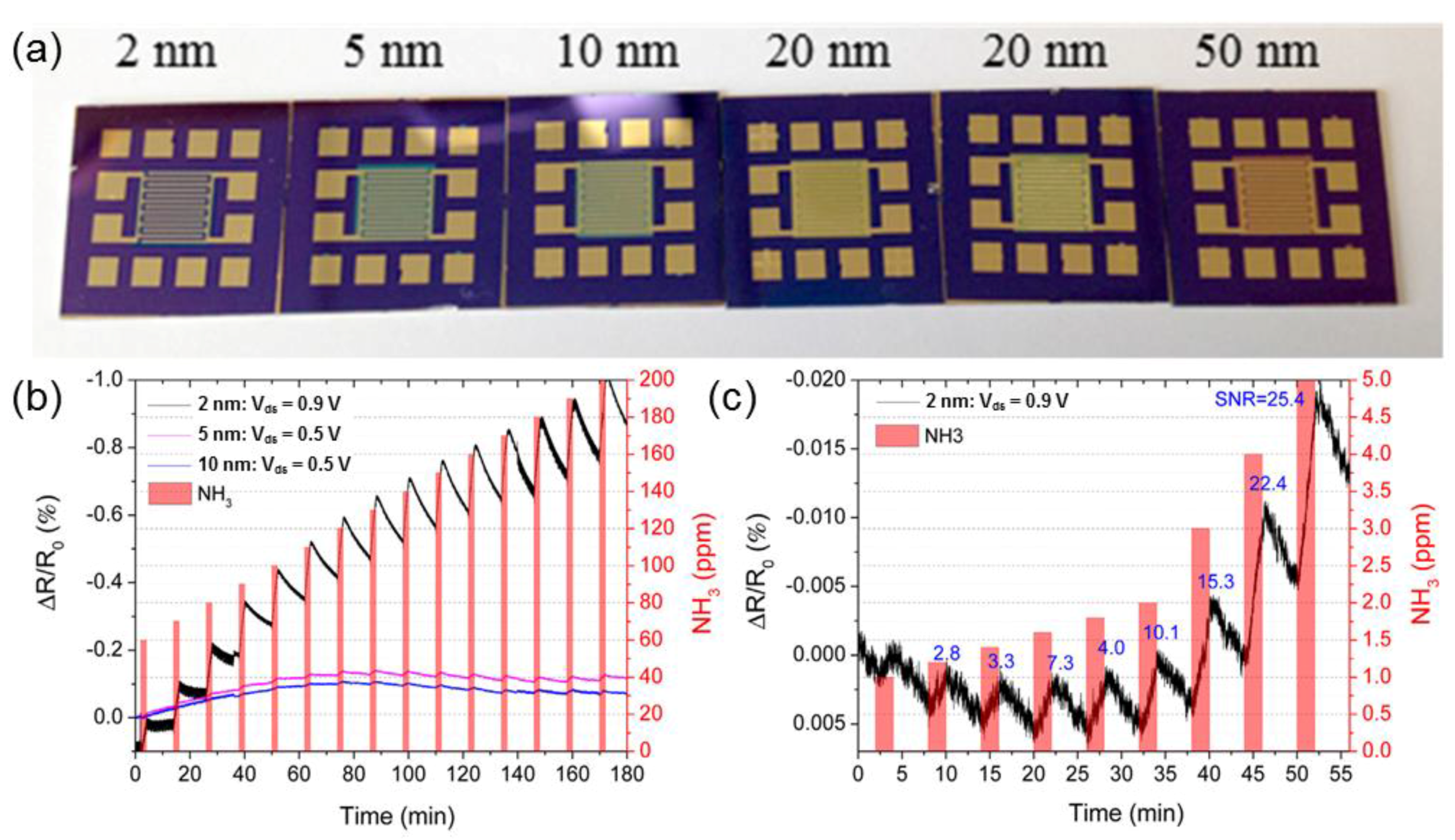
O’Brien et al. reported the aptness of plasma-assisted synthesis of WS2 thin films for sensing applications [37]. The pre-structured WO3 films were deposited on the center of a SiO2 substrate and then sulfurized by the H2S plasma. ICP-activated atmosphere, a mixture of 10% H2S/90% Ar, was introduced to the sputtered films. The plasma was generated in a one-inch quartz tube, which uses a copper coil that is attached to a 13.56-MHz power supply and associated match network. To convert the WO3 to WS2, an exposure time of one hour at 500 °C was used for the synthesizing condition. Then, the IDE electrodes were aligned on top of the WS2 film as shown in Figure 7a. The electrical response of the WS2 films while being exposed to NH3 vapor was measured by continuous observation of the variation in the resistivity of the WS2 films during gas exposure at room temperature. Figure 7b shows the relative resistance change to the initial resistance of the films, which is measured before the NH3 injection. The thicker samples show almost no response to the exposure of NH3, which can be attributed to the existence of oxides. Meanwhile, the 2-, 5- and 10-nm devices exhibit a small increase in conductivity to the exposure of NH3. This means that NH3 gives a charge to the WS2 channel and indicates that the WS2 thin films tested in this experiment show n-type semiconductor behaviors, similar to the bulk crystals [20,26,38,39]. This indicates that the gas sensors based on WS2 have the potential to have selectivity for specific gas molecules, as they exhibit distinguishing properties in charge transfer to WS2 due to their difference in tendency of donating or accepting charge from the WS2 surface. The 2-nm device exhibits a superior response to NH3 exposure, but electrical noise is observed, which is not found in 5- and 10-nm devices. Figure 7c shows the response curves of the 2-nm gas sensor at various concentrations from 1–5 ppm (parts-per-million) of NH3 exposure.
The improved gas-sensing properties of 2D WS2 nanosheets through Ag nanowires (NW) functionalization was demonstrated by Ko et al. [40]. WS2 nanosheets with a large area and Ag NWs were synthesized by the sulfurization process of atomic layer deposition (ALD) with WO3 and a modified CuCl2-mediated polyol process, respectively [41,42]. Ag NW-functionalized (ANF) WS2 was formed through spin-coating using the Ag NWs above. The gas sensors were fabricated with thermally evaporated metal contacts (Cr 5 nm, Au 50 nm). The gas sensing properties were measured at 100 °C. Figure 8a,b shows the gas-sensing property of the ANF WS2 gas sensor with a 4L WS2 nanosheet. After Ag NW functionalization, a current level of 4L WS2 gas sensor exhibits a result approximately two orders lower than that of the pristine WS2 gas sensor. ANF WS2 gas sensors consisting of 1L and 2L WS2 show similar results compared to those of the pristine WS2 sensor. This lowered current of ANF WS2 gas sensors is probably attributed to the n-type doping effect caused by the electrons transferred from Ag NWs to WS2 [43,44,45]. As shown in Figure 8c, the pristine and ANF 4L WS2 gas sensors show a high percent recovery greater than 90%, which implies good recovery to acetone sensing. On the other hand, as shown in Figure 8d, the pristine WS2 gas sensor exhibits relatively low percent recovery ranging from 15%–82% for NO2 exposure (25–500 ppm). However, the ANF 4L WS2 gas sensor shows significantly improved percent recovery for NO2 sensing (over 90%) because the low surface energy of Ag enhances the chemisorption of nitrogen and oxygen species on the Ag surface during the recovery process [46].
An ammonia sensor based on WS2 nanoflakes was reported by Li et al., which showed a remarkable performance at room temperature [47]. Compared to other materials including MoS2, the WS2 nanoflake sensor exhibited good and full recovery. The response and recovery time was 120 s and 150 s, respectively. It seems that a lower adsorption energy of W4+ in the WS2 for ammonia caused by a larger radius results in the faster recovery. The sensor exhibits a high selectivity to other gases such as ethanol, methanol, acetone, benzene and formaldehyde with almost no responses in the air with a humidity of 40%.
2.4. Tin Disulfide
The crystal phase of tin disulfide (SnS2) exists in a layer structure [48]. This phase consists of Sn atoms and sulfur atoms; the Sn atoms are sandwiched between two layers of closely-packed sulfur atoms, which are disposed hexagonally. The neighbor sulfur layers are linked by the weak van der Waals forces (Figure 9a). SnS2 has a larger electronegativity, so it has the potential to increase gas adsorption sites compared to 2D MoS2 [49]. Due to the relatively high temperature dependency on the electronic band structure of SnS2, it is able to be used as an optimizing sensing response and be used for up stepping recovery kinetics at a range of fair elevated temperatures [50,51].
Ou et al. presented an important progress for selective and reversible NO2 sensing based on the charge transfer between physisorbed NO2 gas molecules and two-dimensional (2D) tin disulfide (SnS2) flakes at low operating temperatures [52]. The preparation of 2D SnS2 flakes was done by a wet chemical synthesis technique, and an HRTEM image is shown in Figure 9b. Dropcasting was used for the fabrication of the 2D SnS2 gas sensors. The solution containing 2D SnS2 flakes was dropcast on the substrates made of alumina with interdigitated electrode (IDE) patterns on the surface. As shown in Figure 9c, the sensor exposed to the NO2 gas with concentrations ranging from 0.6–10 ppm has dynamic performance at the optimum operation temperature of 120 °C. As the concentration of NO2 increases, more surface dipoles are formed before the NO2 coverage reaches its maximum, which results in more electron transfer from SnS2 to NO2. Excellent sensor reversibility is observed with a recovery time of less than 180 s at the optimum operating temperature regardless of the NO2 concentration. From this work, the 2D SnS2 flakes showed strong selectivity to NO2, as it has only minimal responses toward other gases. At 120 °C, response factors at industrially-meaningful concentrations for H2 (1%), CH4 (10%), CO2 (10%) and H2S (56 ppm) are found to be ~1.0, ~1.1, ~1.1 and ~1.3, respectively, in comparison to ~36 for NO2 (10 ppm) (Figure 9d). The unique selectivity is formed by the strong physical affinity of paramagnetic NO2 gas molecules toward SnS2 surfaces. Furthermore, there is a relatively preferred position between the Fermi level of SnS2 and partially occupied molecular orbitals (POMO) of NO2.
2.5. Tantalum Disulfide
Tantalum disulfide displays a similar structure to molybdenum disulfide. It has a number of polytypes with a tantalum atom either in trigonal prismatic or octahedral coordination and a number of different stacking orders. All of these types are layered structures with three-coordinate sulfide centers and trigonal prismatic metal centers.
He et al. reported a dosage meter for toxic gas based on TaS2 nanosheets [53]. The TaS2 thin film is prepared via the vacuum filtration of TaS2 aqueous suspension obtained from the electrochemical lithium-intercalation method [54,55,56]. The fabrication of a planar chemoresistive sensor was processed by placing the TaS2 strip (rectangular shaped) onto Si/SiO2 (300 nm) substrate. Then, the deposition of silver paint on both ends of the rectangularly-shaped strip was done for the use of drain and source electrodes. The TaS2 gas sensing performance was evaluated by the conditions of bias of 0.4 V at room temperature, exposing to NO gas with controlling the concentration. The device performed a current response of the NO exposure irreversibly. Furthermore, there was no current recovery at all, even after a long time purge with N2 or heating the sample. At very low concentrations, the sensor based on TaS2 film showed a linear current response and responded immediately towards the change of concentration. Due to these properties, detecting the total dosage of NO under fluctuating concentration is possible. Figure 10a shows the current responses of TaS2 devices against NO exposure at different concentrations for 10 min. The current response and the NO concentration have a quasi-linear relation at ppm level, as shown in Figure 10b. Due to this linear current profile, the TaS2 sensor can realize the integration of the total dosage of NO at fluctuating concentration. The current responses of a typical TaS2 device upon continuous exposure of NO at five different concentrations were tested (Figure 10c). The rate of current decrease (or the sensitivity of the device) increased with the escalation of NO concentration from 0.19 ppm to 4.9 ppm. The linear relation between the current response and the total toxic load for the TaS2 device was demonstrated. (Figure 10d). Thus, the TaS2-based device meets the requirements for a dosage meter. From the current profile, total toxic load can be directly read out. Since the current response upon NO exposure is irreversible, it is available to record the toxic load of NO gas continuously in the sub-ppm level.
2.6. Heterojunction
Previous theoretical studies have reported that heterojunctions with some transition metal disulfide monolayers can align their band structures to be suitable for potential application in versatile applications. The investigations have demonstrated that the monolayer of transition metal disulfide sheets is a sensitive detector for various gas molecules due to the change in the resistivity by the gas adsorption. It is expected that the heterojunctions have electrical resistivity changes by the adsorption of molecules especially on the in-plane interfaces.
Xu et al. have revealed the roles of the heterogeneous interface in the gas sensing properties of SnO2-SnS2 hybrids to ammonia at room temperature [57]. SnS2-SnO2 hybrids are synthesized by oxidizing pristine SnS2 in air at 300 °C with different times from 0.5–4 h (Figure 11a,b). To form a suspension of SnS2 nanosheets, they were dispersed uniformly in ethanol by ultrasonication for 15 min. The suspension was dropcast onto the Au interdigitated electrodes. The sensors were named as SnO2-SnS2-X, where X indicates the different oxidation time in hours. The inset of Figure 11c shows the responses of the sensors, which are measured by the Ig/Ia (represent the current in NH3 and dry air) values. The response of the sensors initially increases and then decreases from SnO2-SnS2-0.5 to SnO2-SnS2-4. The maximum is for SnO2-SnS2-1. The evolution of chemical bonds has the same change trend, which indicates that the performance of the gas-sensing is highly dependent on the number of chemical bonds at the interface. SnO2-SnS2-0.5, SnO2-SnS2-1 and SnO2-SnS2-2 also show good reproducibility and quick response. The typical response recovery characteristics of SnO2-SnS2-0.5, SnO2-SnS2-1 and SnO2-SnS2-2 to 100 ppm of NH3, which appear moderately reproducible, are shown in Figure 11c. Figure 11d indicates the response and recovery characteristics of SnO2-SnS2-1 to NH3 with concentrations of 10, 25, 50, 100, 200 and 500 ppm at room temperature. The sensitivity and reproducibility characteristics of the sensor both show high performance when exposed to various NH3 concentrations. The response is about 1.16 to the exposure of 10 ppm NH3, which indicates that a low detecting limit can be achieved by using SnO2-SnS2 hybrids as the gas sensing material. The comparison of the series of SnO2-SnS2 hybrids oxidized for the time range of 0.5–4 h verifies the dependence between the response of SnO2-SnS2 hybrids to NH3 at room temperature and the interface positioned chemical bonds.
Gu et al. demonstrated a gas sensor based on the SnO2/SnS2 heterojunction, which has a significant response to the exposure of NO2 at low temperature of 80 °C [58]. The heterojunctions were prepared by the in situ high temperature oxidation method, and the SnO2 nanoparticle-decorated SnS2 sensor showed better performance to the exposure of NO2 than the pristine SnS2, such as higher response, lower operating temperature and better selectivity toward other gas molecules.
3. Challenges
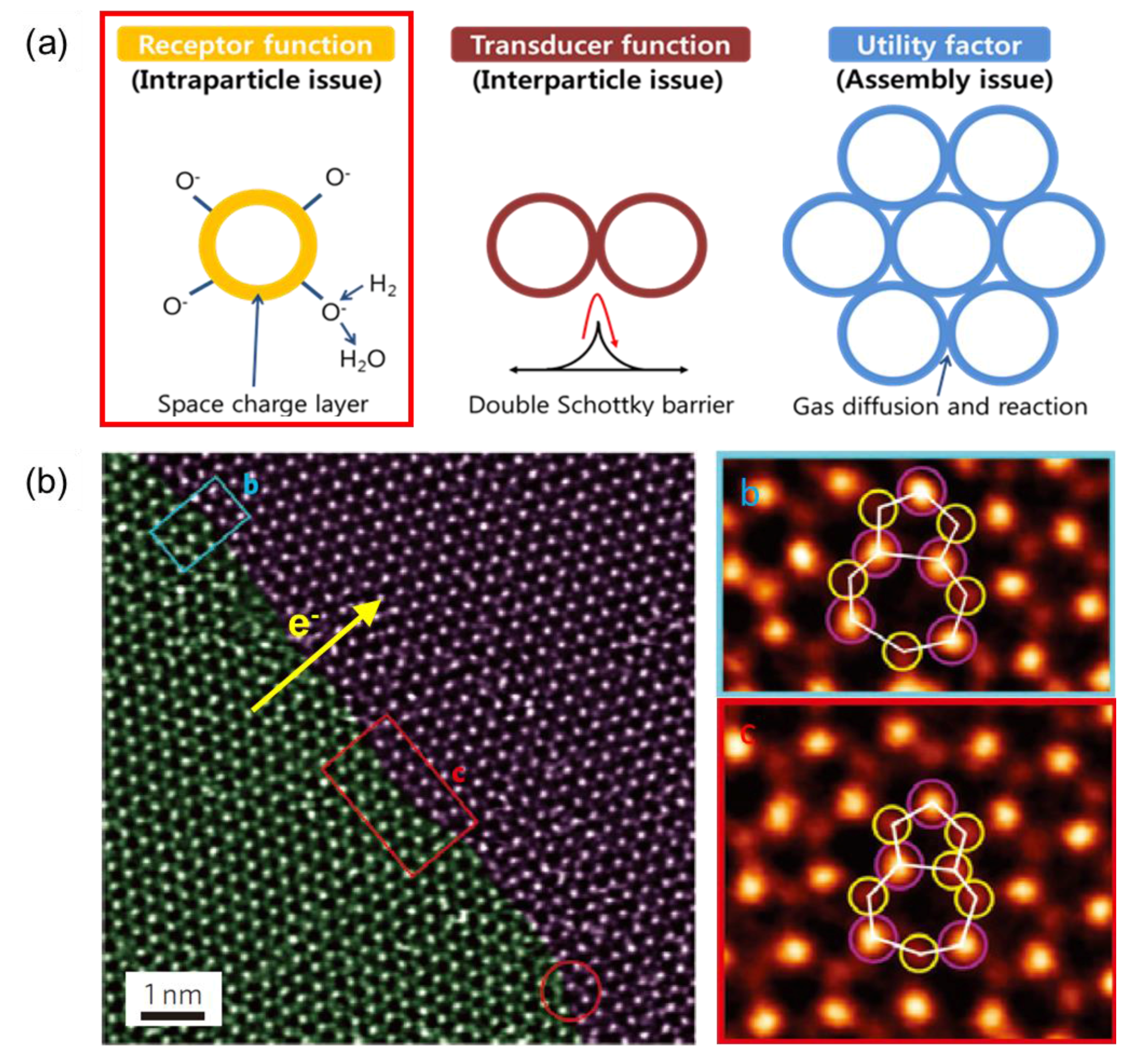
The sensing mechanism of 2D transition metal disulfides gas sensors is based on a charge transfer process [59,60,61]. When the sensors are exposed to reactive gas, the gas molecules are adsorbed (mainly physically at temperatures lower than 100 °C) on the surfaces of 2D transition metal disulfide materials resulting in the variation of sensor resistance. The gas adsorption and the consequent resistance change are affected by three basic factors, namely receptor function, transducer function and utility factor (Figure 12a) [62,63,64,65,66,67]. The receptor function is concerned with how each particle (grain) responds to the adsorbed gas, so it is closely related to the sensitivity and selectivity of the gas sensor [68]. When catalysts are incorporated on the surface of each particle, the gas adsorption and the sequential charge transfer can be enhanced. For the selective adsorption of specific gas molecules, the adoption of appropriate catalysts is very important. The transducer function is related to how the variation of each particle is transduced into device resistance. The transducer function is played by the contacts between each particle. A typical gas sensing strategy that is suggested based on this recognition and the concepts from other traditional semiconductor devices is composed of electron depletion of the particles and double Schottky barrier formation across the contact, as shown in Figure 12a. The utility factor explains how the resistance change is attenuated in an actual porous sensing body with the dissipation of the target gas while it diffuses in to the sensing sites. To maximize the utility factor, the sensing film should be very porous, and then, the target gas molecules diffuse into the bottom layer of the sensing film where the sensor electrode exists, which leads to the effective resistance variation of the sensing film.
Figure 12b is a scanning transmission electron microscope-annular dark-field (STEM-ADF) image of a MoS2 monolayer, a well-studied material representing transition metal disulfides [69]. The grain boundary and its dislocation cores are highlighted. The boundary has a significant relation to the transducer function. When the electron moves across the boundary, it should overcome the double Schottky barrier between two grains. This means that the pre-existing grain boundaries are transducers where the resistance change by the gas adsorption is amplified. For the monolayer MoS2 film, tailoring the utility factor is meaningless. Since the material is atomically thin, the adsorption of gas molecules is not related to the diffusion through the material inside. In other words, the utility factor is already maximized for the 2D material. Therefore, an appropriate approach to develop high performance gas sensors based on 2D transition metal disulfides is to achieve proper receptors that enhanced the interaction between target gas molecules and the sensing material. Thus, the sensitivity and selectivity of chemoresistive gas sensors based on 2D transition metal disulfides largely rely on the receptors on the sensing materials. The receptors can be incorporated on the material by various methods to decorate the surface such as physical vapor deposition, chemical vapor deposition and wet and dry chemical processes. In addition, the creation of point defects, including dopants and vacancies, in the sensing material can be effective since the defects existing on the surface can act as effective receptors. When multiple receptors that selectively respond to each specific gas molecules are obtained, a sensor array based on 2D transition metal disulfides can be realized, in which various target gases can be detected and monitored for environmental and indoor air quality control [70,71]. Since atomically 2D transition metal disulfides are transparent and flexible, the application of 2D-transition-metal-disulfide-based sensors will find new areas that were not reached by the conventional chemoresistive gas sensors. Developing 3D nanostructures based on 2D transition metal disulfides is promising to increase gas response [72,73].
Most of the previously-performed gas sensor devices based on the 2D transition metal disulfide materials had to be measured under a controlled environment, as the existence of other gases in realistic environmental conditions has an influence on the sensitivity of the sensing devices. Hence, following studies need to focus on achieving gas sensing devices with high sensitivity toward the target gas in practical conditions. Under practical conditions, the humidity poisoning effect by which water vapor adsorption reduces the gas sensing properties for most chemoresistive gas sensors should be considered. The fabrication of reliable gas sensors is one of the most challenging issues. Normally, most of the gas sensors are fabricated by a vapor deposition or microfabrication process. These processes are complicated and time consuming, and a reproducible process dealing with transition metal disulfide materials should be established. Furthermore, displaying the intrinsic properties of the sensing materials can fail. Thus, developing a facile, effective and reliable strategy for gas sensors still remains a huge challenge. The capability of large-scale manufacturing of 2D materials with a large area, constant and better quality and reproducibility is yet another big challenge [12,74].
4. Conclusions
In this article, we review typical 2D transition metal disulfides for gas sensing applications. Transition metal disulfides (MoS2, WS2, SnS2 and TaS2) possess tunable band gaps dependent on their layer thickness, and their excellent advantages in nanostructuring and heterostructuring make them attractive candidates for the fabrication of gas sensors. The results described that 2D transition metal disulfides are suitable materials for the fabrication of high performance gas sensors operated in diverse environments due to their particular characteristics. There are some reports on the theoretical simulations of gas adsorption on transition metal disulfides; still, the works are very limited and lacking. Following research in this field needs to understand the details of the specific properties of nanostructured two-dimensional materials and the change of the electronic properties with the adsorption of analytes to enhance the performance of the gas sensors based on these materials. First-principles calculations can be used to identify the appropriate modification of these materials for the higher performance of the gas sensors. The gas sensing mechanisms of devices based on 2D transition metal disulfides have not been completely explained till now. Once the mechanism is clarified, 2D transition metal disulfides gas sensors could perform significant sensitivity, ultrahigh selectivity, fast response, good reversibility, room temperature operation, outstanding stability, etc., in the near future.
Acknowledgments
This work was financially supported by the Future Material Discovery (NRF-2016M3D1A1027666), the Nano·Material Technology Development Program through the National Research Foundation of Korea (NRF) (2016M3A7B4910) and the International Energy Joint R&D Program of the Korea Institute of Energy Technology Evaluation and Planning (KETEP) (20168510011350).
Author Contributions
T.H.K. and H.W.J. conceived of and wrote the paper. Y.H.K., S.Y.P and S.Y.K. contributed to finding the references.
Conflicts of Interest
The authors declare no conflict of interest.
References
- Swan, M. Sensor mania! The internet of things, wearable computing, objective metrics, and the quantified self 2.0. J. Sens. Actuator Netw. 2012, 1, 217–253. [Google Scholar] [CrossRef]
- Kim, Y.H.; Kim, S.J.; Kim, Y.-J.; Shim, Y.-S.; Kim, S.Y.; Hong, B.H.; Jang, H.W. Self-activated transparent all-graphene gas sensor with endurance to humidity and mechanical bending. ACS Nano 2015, 9, 10453–10460. [Google Scholar] [CrossRef] [PubMed]
- Choi, K.J.; Jang, H.W. One-dimensional oxide nanostructures as gas-sensing materials: Review and issues. Sensors 2010, 10, 4083–4099. [Google Scholar] [CrossRef] [PubMed]
- Jeon, J.-M.; Shim, Y.-S.; Han, S.D.; Kim, D.H.; Kim, Y.H.; Kang, C.-Y.; Kim, J.-S.; Kim, M.; Jang, H.W. Vertically ordered SnO2 nanobamboos for substantially improved detection of volatile reducing gases. J. Mater. Chem. A 2015, 3, 17939–17945. [Google Scholar] [CrossRef]
- Lee, J.-H. Gas sensors using hierarchical and hollow oxide nanostructures: Overview. Sens. Actuators B Chem. 2009, 140, 319–336. [Google Scholar] [CrossRef]
- Suh, J.M.; Shim, Y.S.; Kim, D.H.; Sohn, W.; Jung, Y.; Lee, S.Y.; Choi, S.; Kim, Y.H.; Jeon, J.M.; Hong, K.; et al. Synergetically selective toluene sensing in hematite-decorated nickel oxide nanocorals. Adv. Mater. Technol. 2017, 2, 1600259. [Google Scholar] [CrossRef]
- Yoon, J.-W.; Choi, S.H.; Kim, J.-S.; Jang, H.W.; Kang, Y.C.; Lee, J.-H. Trimodally porous SnO2 nanospheres with three-dimensional interconnectivity and size tunability: A one-pot synthetic route and potential application as an extremely sensitive ethanol detector. NPG Asia Mater. 2016, 8, e244. [Google Scholar] [CrossRef]
- Fowler, J.D.; Allen, M.J.; Tung, V.C.; Yang, Y.; Kaner, R.B.; Weiller, B.H. Practical chemical sensors from chemically derived graphene. ACS Nano 2009, 3, 301–306. [Google Scholar] [CrossRef] [PubMed]
- Li, H.; Wu, J.; Yin, Z.; Zhang, H. Preparation and applications of mechanically exfoliated single-layer and multilayer MoS2 and WSe2 nanosheets. Acc. Chem. Res. 2014, 47, 1067–1075. [Google Scholar] [CrossRef] [PubMed]
- Robinson, J.T.; Perkins, F.K.; Snow, E.S.; Wei, Z.; Sheehan, P.E. Reduced graphene oxide molecular sensors. Nano Lett. 2008, 8, 3137–3140. [Google Scholar] [CrossRef] [PubMed]
- Schedin, F.; Geim, A.; Morozov, S.; Hill, E.; Blake, P.; Katsnelson, M.; Novoselov, K. Detection of individual gas molecules adsorbed on graphene. Nat. Mater. 2007, 6, 652–655. [Google Scholar] [CrossRef] [PubMed]
- Chhowalla, M.; Shin, H.S.; Eda, G.; Li, L.-J.; Loh, K.P.; Zhang, H. The chemistry of two-dimensional layered transition metal dichalcogenide nanosheets. Nat. Chem. 2013, 5, 263–275. [Google Scholar] [CrossRef] [PubMed]
- Andoshe, D.M.; Jeon, J.-M.; Kim, S.Y.; Jang, H.W. Two-dimensional transition metal dichalcogenide nanomaterials for solar water splitting. Electron. Mater. Lett. 2015, 11, 323–335. [Google Scholar] [CrossRef]
- Topsøe, H.; Clausen, B.S.; Massoth, F.E. Hydrotreating catalysis. In Catalysis; Springer: Berlin/Heidelberg, Germany, 1996; pp. 1–269. [Google Scholar]
- Mak, K.F.; Lee, C.; Hone, J.; Shan, J.; Heinz, T.F. Atomically thin MoS2: A new direct-gap semiconductor. Phys. Rev. Lett. 2010, 105, 136805. [Google Scholar] [CrossRef] [PubMed]
- Splendiani, A.; Sun, L.; Zhang, Y.; Li, T.; Kim, J.; Chim, C.-Y.; Galli, G.; Wang, F. Emerging photoluminescence in monolayer MoS2. Nano Lett. 2010, 10, 1271–1275. [Google Scholar] [CrossRef] [PubMed]
- Radisavljevic, B.; Radenovic, A.; Brivio, J.; Giacometti, I.V.; Kis, A. Single-layer MoS2 transistors. Nat. Nanotechnol. 2011, 6, 147–150. [Google Scholar] [CrossRef] [PubMed]
- Yin, Z.; Li, H.; Li, H.; Jiang, L.; Shi, Y.; Sun, Y.; Lu, G.; Zhang, Q.; Chen, X.; Zhang, H. Single-layer MoS2 phototransistors. ACS Nano 2011, 6, 74–80. [Google Scholar] [CrossRef] [PubMed]
- Lee, H.S.; Min, S.-W.; Chang, Y.-G.; Park, M.K.; Nam, T.; Kim, H.; Kim, J.H.; Ryu, S.; Im, S. MoS2 nanosheet phototransistors with thickness-modulated optical energy gap. Nano Lett. 2012, 12, 3695–3700. [Google Scholar] [CrossRef] [PubMed]
- Li, H.; Yin, Z.; He, Q.; Li, H.; Huang, X.; Lu, G.; Fam, D.W.H.; Tok, A.I.Y.; Zhang, Q.; Zhang, H. Fabrication of single- and multilayer MoS2 film-based field-effect transistors for sensing no at room temperature. Small 2012, 8, 63–67. [Google Scholar] [CrossRef] [PubMed]
- Lee, C.; Yan, H.; Brus, L.E.; Heinz, T.F.; Hone, J.; Ryu, S. Anomalous lattice vibrations of single-and few-layer MoS2. ACS Nano 2010, 4, 2695–2700. [Google Scholar] [CrossRef] [PubMed]
- Novoselov, K.; Jiang, D.; Schedin, F.; Booth, T.; Khotkevich, V.; Morozov, S.; Geim, A. Two-dimensional atomic crystals. Proc. Natl. Acad. Sci. USA 2005, 102, 10451–10453. [Google Scholar] [CrossRef] [PubMed]
- Li, W.; Geng, X.; Guo, Y.; Rong, J.; Gong, Y.; Wu, L.; Zhang, X.; Li, P.; Xu, J.; Cheng, G.; et al. Reduced graphene oxide electrically contacted graphene sensor for highly sensitive nitric oxide detection. ACS Nano 2011, 5, 6955–6961. [Google Scholar] [CrossRef] [PubMed]
- Leenaerts, O.; Partoens, B.; Peeters, F. Adsorption of H2O, NH3, CO, NO2, and NO on graphene: A first-principles study. Phys. Rev. B 2008, 77, 125416. [Google Scholar] [CrossRef]
- Zhang, J.; Boyd, A.; Tselev, A.; Paranjape, M.; Barbara, P. Mechanism of NO2 detection in carbon nanotube field effect transistor chemical sensors. Appl. Phys. Lett. 2006, 88. [Google Scholar] [CrossRef]
- Perkins, F.K.; Friedman, A.L.; Cobas, E.; Campbell, P.; Jernigan, G.; Jonker, B.T. Chemical vapor sensing with monolayer MoS2. Nano Lett. 2013, 13, 668–673. [Google Scholar] [CrossRef] [PubMed]
- Late, D.J.; Huang, Y.-K.; Liu, B.; Acharya, J.; Shirodkar, S.N.; Luo, J.; Yan, A.; Charles, D.; Waghmare, U.V.; Dravid, V.P.; et al. Sensing behavior of atomically thin-layered MoS2 transistors. ACS Nano 2013, 7, 4879–4891. [Google Scholar] [CrossRef] [PubMed]
- Kim, Y.H.; Kim, K.Y.; Choi, Y.R.; Shim, Y.-S.; Jeon, J.-M.; Lee, J.-H.; Kim, S.Y.; Han, S.; Jang, H.W. Ultrasensitive reversible oxygen sensing by using liquid-exfoliated MoS2 nanoparticles. J. Mater. Chem. A 2016, 4, 6070–6076. [Google Scholar] [CrossRef]
- Bollinger, M.; Lauritsen, J.; Jacobsen, K.W.; Nørskov, J.K.; Helveg, S.; Besenbacher, F. One-dimensional metallic edge states in MoS2. Phys. Rev. Lett. 2001, 87, 196803. [Google Scholar] [CrossRef] [PubMed]
- Chen, Y.; Xue, X.; Wang, Y.; Wang, T. Synthesis and ethanol sensing characteristics of single crystalline SnO2 nanorods. Appl. Phys. Lett. 2005, 87, 233503. [Google Scholar] [CrossRef]
- Gao, T.; Wang, T. Synthesis and properties of multipod-shaped ZnO nanorods for gas-sensor applications. Appl. Phys. A Mater. 2005, 80, 1451–1454. [Google Scholar] [CrossRef]
- Hsueh, T.-J.; Hsu, C.-L.; Chang, S.-J.; Chen, I.-C. Laterally grown ZnO nanowire ethanol gas sensors. Sens. Actuators B Chem. 2007, 126, 473–477. [Google Scholar] [CrossRef]
- Liang, Y.; Chen, Y.; Wang, T. Low-resistance gas sensors fabricated from multiwalled carbon nanotubes coated with a thin tin oxide layer. Appl. Phys. Lett. 2004, 85, 666–668. [Google Scholar] [CrossRef]
- Scott, R.W.; Yang, S.; Chabanis, G.; Coombs, N.; Williams, D.; Ozin, G. Tin dioxide opals and inverted opals: Near-ideal microstructures for gas sensors. Adv. Mater. 2001, 13, 1468–1472. [Google Scholar] [CrossRef]
- Shimizu, Y.; Egashira, M. Basic aspects and challenges of semiconductor gas sensors. MRS Bull. 1999, 24, 18–24. [Google Scholar] [CrossRef]
- Wan, Q.; Li, Q.; Chen, Y.; Wang, T.-H.; He, X.; Li, J.; Lin, C. Fabrication and ethanol sensing characteristics of ZnO nanowire gas sensors. Appl. Phys. Lett. 2004, 84, 3654–3656. [Google Scholar] [CrossRef]
- O’Brien, M.; Lee, K.; Morrish, R.; Berner, N.C.; McEvoy, N.; Wolden, C.A.; Duesberg, G.S. Plasma assisted synthesis of WS2 for gas sensing applications. Chem. Phys. Lett. 2014, 615, 6–10. [Google Scholar] [CrossRef]
- He, Q.; Zeng, Z.; Yin, Z.; Li, H.; Wu, S.; Huang, X.; Zhang, H. Fabrication of flexible MoS2 thin film transistor arrays for practical gas sensing applications. Small 2012, 8, 2994–2999. [Google Scholar] [CrossRef] [PubMed]
- Lee, K.; Gatensby, R.; McEvoy, N.; Hallam, T.; Duesberg, G.S. High-performance sensors based on molybdenum disulfide thin films. Adv. Mater. 2013, 25, 6699–6702. [Google Scholar] [CrossRef] [PubMed]
- Ko, K.Y.; Song, J.-G.; Kim, Y.; Choi, T.; Shin, S.; Lee, C.W.; Lee, K.; Koo, J.; Lee, H.; Kim, J.; et al. Improvement of gas-sensing performance of large-area tungsten disulfide nanosheets by surface functionalization. ACS Nano 2016, 10, 9287–9296. [Google Scholar] [CrossRef] [PubMed]
- Korte, K.E.; Skrabalak, S.E.; Xia, Y. Rapid synthesis of silver nanowires through a CuCl-or CuCl2-mediated polyol process. J. Mater. Chem. 2008, 18, 437–441. [Google Scholar] [CrossRef]
- Song, J.-G.; Park, J.; Lee, W.; Choi, T.; Jung, H.; Lee, C.W.; Hwang, S.-H.; Myoung, J.M.; Jung, J.-H.; Kim, S.-H.; et al. Layer-controlled, wafer-scale, and conformal synthesis of tungsten disulfide nanosheets using atomic layer deposition. ACS Nano 2013, 7, 11333–11340. [Google Scholar] [CrossRef] [PubMed]
- Choi, M.S.; Qu, D.; Lee, D.; Liu, X.; Watanabe, K.; Taniguchi, T.; Yoo, W.J. Lateral MoS2 p–n junction formed by chemical doping for use in high-performance optoelectronics. ACS Nano 2014, 8, 9332–9340. [Google Scholar] [CrossRef] [PubMed]
- Shi, Y.; Huang, J.-K.; Jin, L.; Hsu, Y.-T.; Yu, S.F.; Li, L.-J.; Yang, H.Y. Selective decoration of Au nanoparticles on monolayer MoS2 single crystals. Sci. Rep. 2013, 3, 1839. [Google Scholar] [CrossRef] [PubMed]
- Yang, L.; Majumdar, K.; Liu, H.; Du, Y.; Wu, H.; Hatzistergos, M.; Hung, P.; Tieckelmann, R.; Tsai, W.; Hobbs, C.; et al. Chloride molecular doping technique on 2D materials: WS2 and MoS2. Nano Lett. 2014, 14, 6275–6280. [Google Scholar] [CrossRef] [PubMed]
- Choi, S.-W.; Katoch, A.; Sun, G.-J.; Wu, P.; Kim, S.S. NO2 sensing performance of SnO2 microrods by functionalization of Ag nanoparticles. J. Mater. Chem. C 2013, 1, 2834–2841. [Google Scholar] [CrossRef]
- Li, X.; Li, X.; Li, Z.; Wang, J.; Zhang, J. WS2 nanoflakes based selective ammonia sensors at room temperature. Sens. Actuators B Chem. 2017, 240, 273–277. [Google Scholar] [CrossRef]
- Julien, C.; Eddrief, M.; Samaras, I.; Balkanski, M. Optical and electrical characterizations of SnSe, SnS2 and SnSe2 single crystals. Mater. Sci. Eng. B 1992, 15, 70–72. [Google Scholar] [CrossRef]
- Xu, Y.; Schoonen, M.A. The absolute energy positions of conduction and valence bands of selected semiconducting minerals. Am. Mineral. 2000, 85, 543–556. [Google Scholar] [CrossRef]
- El-Mahalawy, S.; Evans, B. Temperature dependence of the electrical conductivity and hall coefficient in 2H-MoS2, MoSe2, WSe2, and MoTe2. Phys. Status Solidi B 1977, 79, 713–722. [Google Scholar] [CrossRef]
- Patil, S.; Tredgold, R. Electrical and photoconductive properties of SnS2 crystals. J. Phys. D Appl. Phys. 1971, 4, 718. [Google Scholar] [CrossRef]
- Ou, J.Z.; Ge, W.; Carey, B.; Daeneke, T.; Rotbart, A.; Shan, W.; Wang, Y.; Fu, Z.; Chrimes, A.F.; Wlodarski, W.; et al. Physisorption-based charge transfer in two-dimensional SnS2 for selective and reversible NO2 gas sensing. ACS Nano 2015, 9, 10313–10323. [Google Scholar] [CrossRef] [PubMed]
- He, Q.; Ma, Q.; Chen, B.; Yin, Z.; Zeng, Z.; Wu, S.; Cao, X.; Kong, X.; Zhang, H. TaS2 nanosheet-based room-temperature dosage meter for nitric oxide. APL Mater. 2014, 2, 092506. [Google Scholar] [CrossRef]
- Huang, X.; Zeng, Z.; Zhang, H. Metal dichalcogenide nanosheets: Preparation, properties and applications. Chem. Soc. Rev. 2013, 42, 1934–1946. [Google Scholar] [CrossRef] [PubMed]
- Zeng, Z.; Sun, T.; Zhu, J.; Huang, X.; Yin, Z.; Lu, G.; Fan, Z.; Yan, Q.; Hng, H.H.; Zhang, H. An effective method for the fabrication of few-layer-thick inorganic nanosheets. Angew. Chem. Int. Ed. 2012, 51, 9052–9056. [Google Scholar] [CrossRef] [PubMed]
- Zeng, Z.; Yin, Z.; Huang, X.; Li, H.; He, Q.; Lu, G.; Boey, F.; Zhang, H. Single-layer semiconducting nanosheets: High-yield preparation and device fabrication. Angew. Chem. Int. Ed. 2011, 50, 11093–11097. [Google Scholar] [CrossRef] [PubMed]
- Xu, K.; Li, N.; Zeng, D.; Tian, S.; Zhang, S.; Hu, D.; Xie, C. Interface bonds determined gas-sensing of SnO2-SnS2 hybrids to ammonia at room temperature. ACS Appl. Mater. Interfaces 2015, 7, 11359–11368. [Google Scholar] [CrossRef] [PubMed]
- Gu, D.; Li, X.; Zhao, Y.; Wang, J. Enhanced NO2 sensing of SnO2/SnS2 heterojunction based sensor. Sens. Actuators B Chem. 2017, 244, 67–76. [Google Scholar] [CrossRef]
- Cho, B.; Hahm, M.G.; Choi, M.; Yoon, J.; Kim, A.R.; Lee, Y.-J.; Park, S.-G.; Kwon, J.-D.; Kim, C.S.; Song, M.; et al. Charge-transfer-based gas sensing using atomic-layer MoS2. Sci. Rep. 2015, 5, 8052. [Google Scholar] [CrossRef] [PubMed]
- Liu, B.; Chen, L.; Liu, G.; Abbas, A.N.; Fathi, M.; Zhou, C. High-performance chemical sensing using schottky-contacted chemical vapor deposition grown monolayer MoS2 transistors. ACS Nano 2014, 8, 5304–5314. [Google Scholar] [CrossRef] [PubMed]
- Yuan, W.; Liu, A.; Huang, L.; Li, C.; Shi, G. High-performance NO2 sensors based on chemically modified graphene. Adv. Mater. 2013, 25, 766–771. [Google Scholar] [CrossRef] [PubMed]
- Matsunaga, N.; Sakai, G.; Shimanoe, K.; Yamazoe, N. Diffusion equation-based study of thin film semiconductor gas sensor-response transient. Sens. Actuators B Chem. 2002, 83, 216–221. [Google Scholar] [CrossRef]
- Sakai, G.; Matsunaga, N.; Shimanoe, K.; Yamazoe, N. Theory of gas-diffusion controlled sensitivity for thin film semiconductor gas sensor. Sens. Actuators B Chem. 2001, 80, 125–131. [Google Scholar] [CrossRef]
- Yamazoe, N.; Shimanoe, K. Roles of shape and size of component crystals in semiconductor gas sensors I. Response to oxygen. J. Electrochem. Soc. 2008, 155, J85–J92. [Google Scholar] [CrossRef]
- Yamazoe, N.; Shimanoe, K. Roles of shape and size of component crystals in semiconductor gas sensors II. Response to NO2 and H2. J. Electrochem. Soc. 2008, 155, J93–J98. [Google Scholar] [CrossRef]
- Yamazoe, N.; Shimanoe, K.; Sawada, C. Contribution of electron tunneling transport in semiconductor gas sensor. Thin Solid Films 2007, 515, 8302–8309. [Google Scholar] [CrossRef]
- Barsan, N.; Koziej, D.; Weimar, U. Metal oxide-based gas sensor research: How to? Sens. Actuators B Chem. 2007, 121, 18–35. [Google Scholar] [CrossRef]
- Yamazoe, N.; Shimanoe, K. New perspectives of gas sensor technology. Sens. Actuators B Chem. 2009, 138, 100–107. [Google Scholar] [CrossRef]
- Najmaei, S.; Liu, Z.; Zhou, W.; Zou, X.; Shi, G.; Lei, S.; Yakobson, B.I.; Idrobo, J.-C.; Ajayan, P.M.; Lou, J. Vapour phase growth and grain boundary structure of molybdenum disulphide atomic layers. Nat. Mater. 2013, 12, 754–759. [Google Scholar] [CrossRef] [PubMed]
- Hwang, S.; Kwon, H.; Chhajed, S.; Byon, J.W.; Baik, J.M.; Im, J.; Oh, S.H.; Jang, H.W.; Yoon, S.J.; Kim, J.K. A near single crystalline TiO2 nanohelix array: Enhanced gas sensing performance and its application as a monolithically integrated electronic nose. Analyst 2013, 138, 443–450. [Google Scholar] [CrossRef] [PubMed]
- Kim, H.-J.; Yoon, J.-W.; Choi, K.-I.; Jang, H.W.; Umar, A.; Lee, J.-H. Ultraselective and sensitive detection of xylene and toluene for monitoring indoor air pollution using cr-doped nio hierarchical nanostructures. Nanoscale 2013, 5, 7066–7073. [Google Scholar] [CrossRef] [PubMed]
- Varghese, S.S.; Varghese, S.H.; Swaminathan, S.; Singh, K.K.; Mittal, V. Two-dimensional materials for sensing: Graphene and beyond. Electronics 2015, 4, 651–687. [Google Scholar] [CrossRef]
- Yang, W.; Gan, L.; Li, H.; Zhai, T. Two-dimensional layered nanomaterials for gas-sensing applications. Inorg. Chem. Front. 2016, 3, 433–451. [Google Scholar] [CrossRef]
- Kwon, K.C.; Choi, S.; Hong, K.; Moon, C.W.; Shim, Y.-S.; Kim, D.H.; Kim, T.; Sohn, W.; Jeon, J.-M.; Lee, C.-H.; et al. Wafer-scale transferable molybdenum disulfide thin-film catalysts for photoelectrochemical hydrogen production. Energy Environ. Sci. 2016, 9, 2240–2248. [Google Scholar] [CrossRef]
Figure 1.
Structure of monolayered transition metal dichalcogenides. (a) About 40 different layered transition metal dichalcogenide compounds exist. (b,c) c-axis and [11,12,13,14,15,16,17,18,19,20] section view of single-layer transition metal dichalcogenides with trigonal prismatic (b) and octahedral (c) coordinations. Atom color code: purple, metal; yellow, chalcogen. The labels AbA and AbC represent the stacking sequence where the upper- and lower-case letters represent chalcogen and metal elements, respectively (Reproduced with permission of [12]. Copyright Nature Publishing Group, 2013.).

Figure 2.
(a) Number of publications and (b) element forms of 2D transition metal disulfides used for gas sensor applications in the publications since 2011. The publication search was performed on 23 March 2017 using the Science Citation Index Expanded database of the Web of Science provided by Thomson Reuters. All possible keywords from combinations of gas sensor and 2D transition metal disulfides (MoS2, WS2, SnS2, TaS2, TiS2) were used for the search.
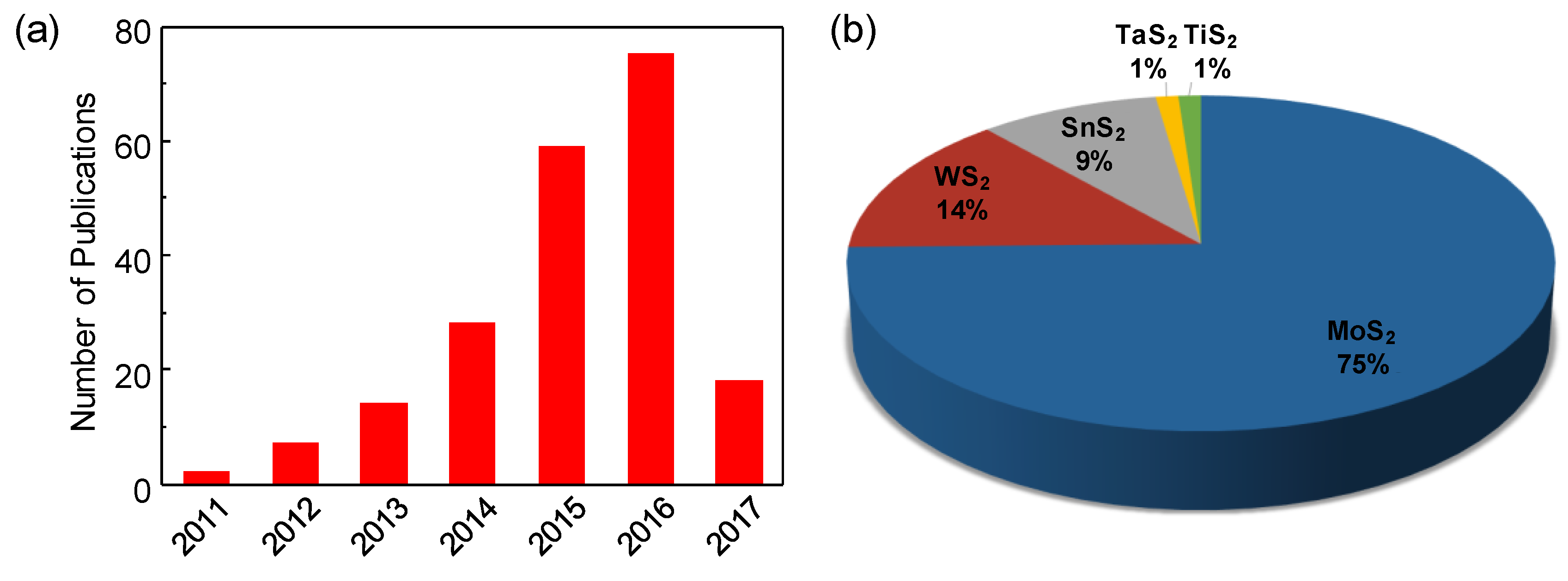
Figure 3.
(a) Optical microscope image of mechanically-exfoliated bilayer MoS2 films on Si/SiO2. (b) AFM image of the bilayer (2L) (thickness: 1.5 nm) MoS2 film. (c) Real-time current response after exposure of the 2L MoS2 FET to NO with increased concentration. Inset: A typical adsorption and desorption process of NO on the 2L MoS2 FET. (d) Plot of the percent change in current as a function of NO concentration (Reproduced with permission of [20]. Copyright John Wiley and Sons, 2011.).

Figure 4.
(a) Schematic of a single monolayer of MoS2 supported on a SiO2/Si substrate and contacted with Au contact pads. (b) An optical image of the processed devices showing the monolayer MoS2 flakes electrically contacted by multiple Au leads. (c) Histogram of MoS2 and CNT-network sensor responses to various analytes. (d) Change in conductivity of the monolayer MoS2 sensor channel upon exposure to a series of pulses in which the TEA concentration increases from 0.002% P0–0.2% P0. (e) Change in conductivity of the monolayer MoS2 sensor channel upon exposure to a sequence of pulses in which the acetone concentration increases from 0.02% P0–2% P0 (black line). (f) Response of sensors to nitrotoluene. The monolayer MoS2 sensor (red line) shows no response to analytes, such as nitrotoluene, which tend to act as acceptors, while the CNT-network sensor (black line) shows a pronounced response. The nitrotoluene concentration increases from 0.01% P0–1% P0 and is shown inverted for convenience to facilitate comparison with the sensor response (Reproduced with permission of [26]. Copyright American Chemical Society, 2013.).
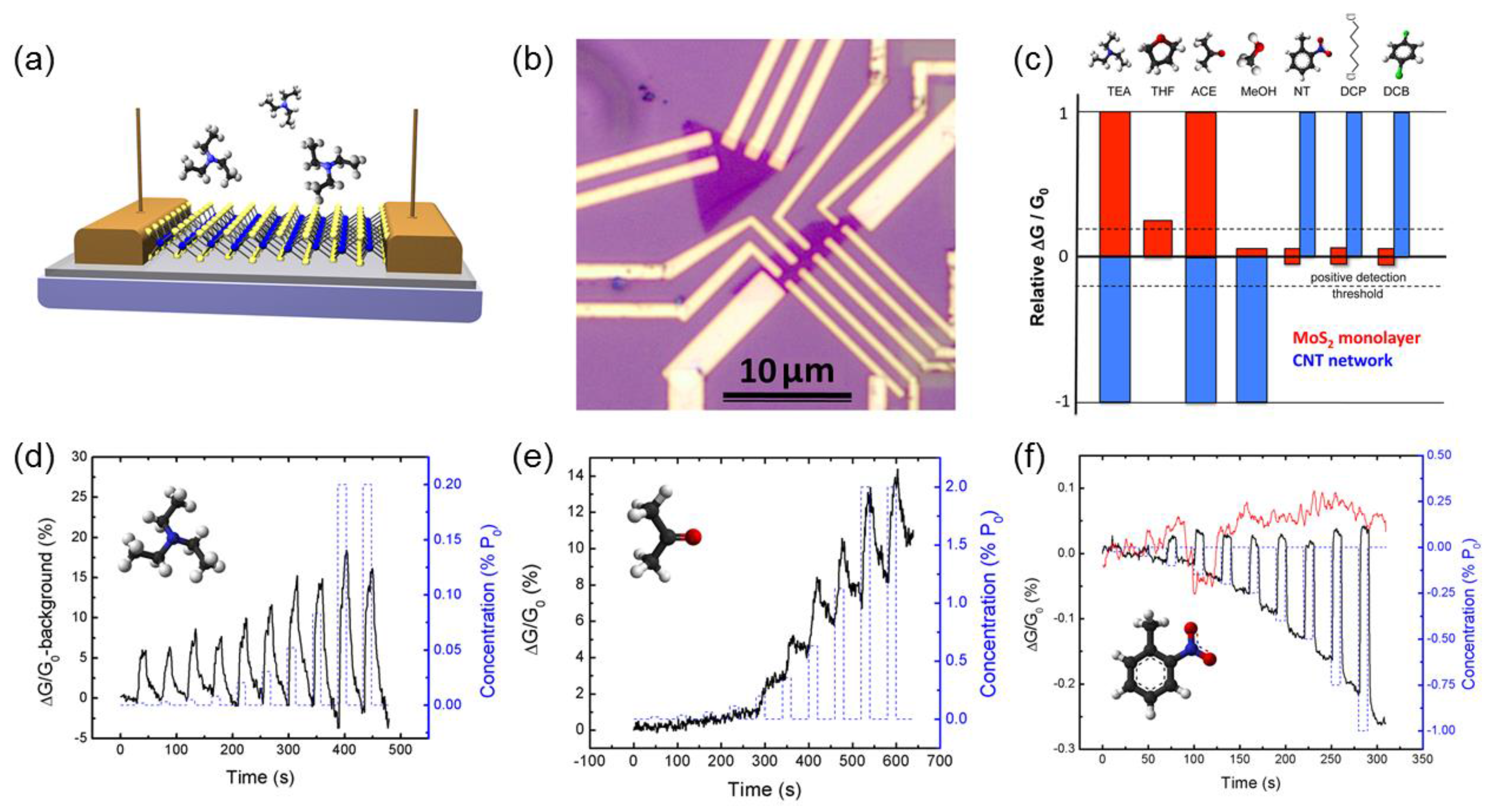
Figure 5.
(a) Schematic of the MoS2 transistor-based NO2 gas-sensing device. (b) Low-magnification TEM image; the inset shows the high-resolution TEM image. (c) Sensitivity as a function of concentration (in ppm) for two-layer and five-layer MoS2 sheets for NH3. (d) Sensitivity as a function of concentration (in ppm) for two-layer and five-layer MoS2 sheets for NO2 (Reproduced with permission of [27]. Copyright American Chemical Society, 2013.).
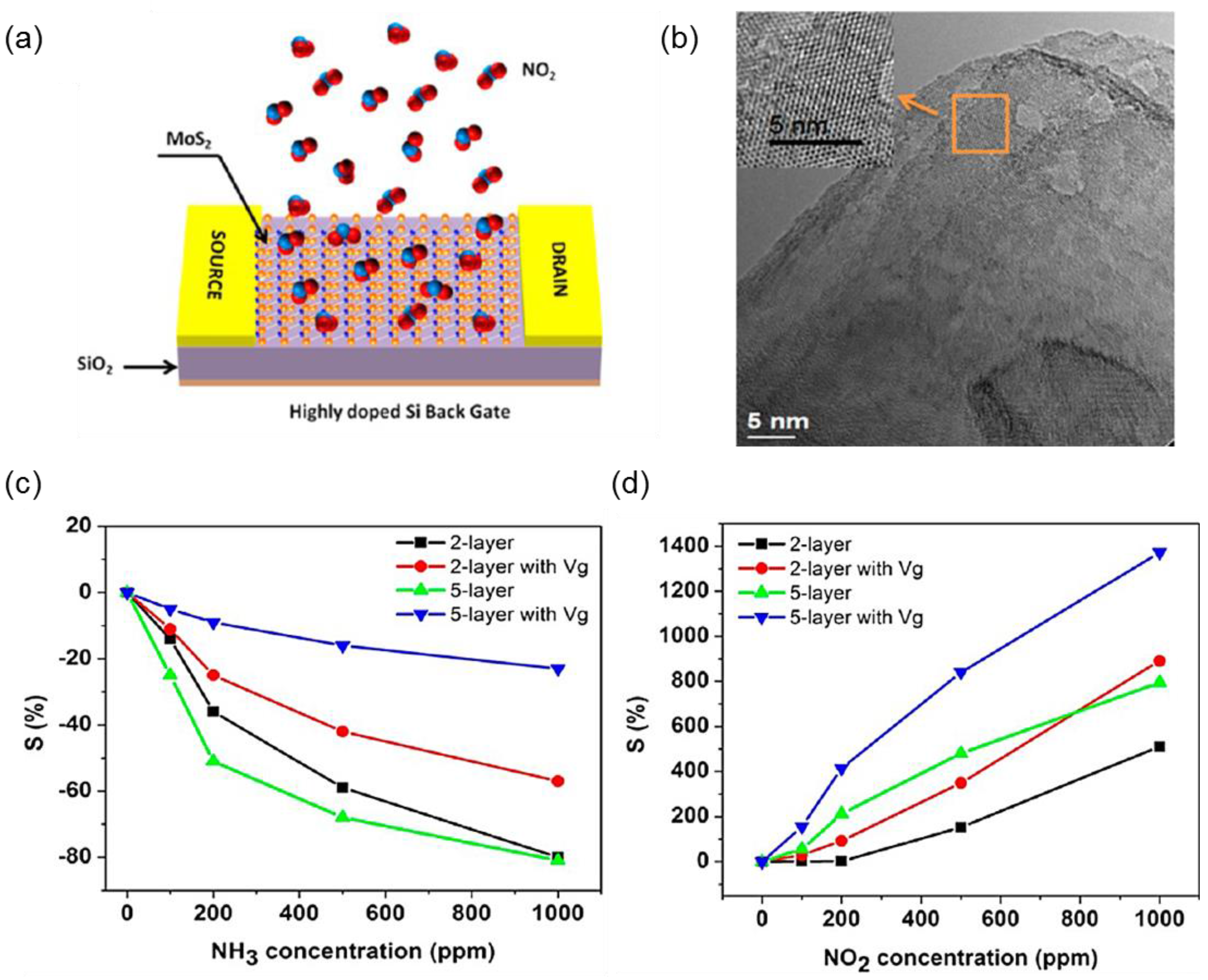
Figure 6.
(a) Response curves of the liquid-exfoliated MoS2 gas sensor to four pulses of 100% of O2 at 300 °C. (b) Response curves to different O2 concentrations at 300 °C. (c) Linear fit of the responses as a function of O2 at 300 °C. (d) Stable sites of O2 adsorption. Locally stable configurations of O2 adsorbed on clean Mo-edges and Mo-edges with S monomers. The adsorption free energy at 300 °C and 1 atm (Gad (300 °C, 1 atm)) is displayed. (e) Band structure, density of states (DOS) of edge atoms and charge density distribution near the Fermi level of clean Mo-edges with S monomers and O2 adsorbed Mo-edges with S monomers on the Mo–S bridge site. The color intensity in the band structure is proportional to the weight of the corresponding state on the edge atoms (Reproduced with permission of [28]. Copyright Royal Society of Chemistry, 2016.).
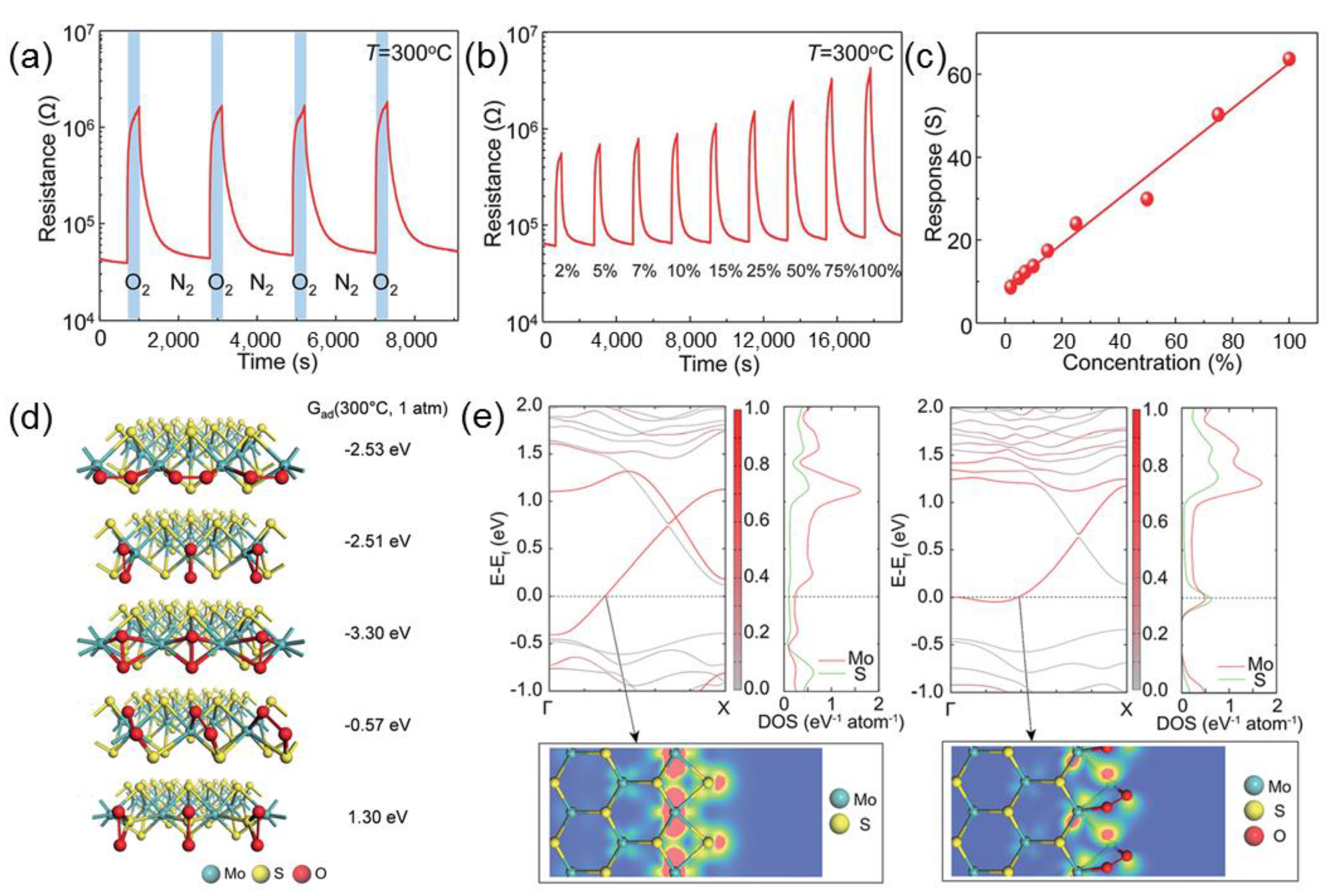
Figure 7.
(a) Optical image of WS2 devices contacted with interdigitated electrodes. (b) Percentile resistance change versus time at given bias voltages for the 2-, 5- and 10-nm WS2 films with NH3 gas injections over 180 min. (c) Percentile resistance change versus time for the 2-nm film at a bias voltage of 0.9 V, upon interval NH3 exposures at various concentrations from 1 ppm–5 ppm (Reproduced with permission of [37]. Copyright Chemical Physics Letters, 2014.).

Figure 8.
Gas-sensing results of the Ag nanowires-functionalized (ANF) WS2 gas sensors consisting of 4L WS2 nanosheet upon (a) acetone exposure (0.5, 1, 2, 4 and 10 ppm) and (b) NO2 exposure (25, 50, 100, 200 and 500 ppm). Percent recovery of the pristine and ANF WS2 gas sensor for (c) acetone and (d) NO2 exposure as a function of gas concentration (Reproduced with permission of [40]. Copyright American Chemical Society, 2016.).
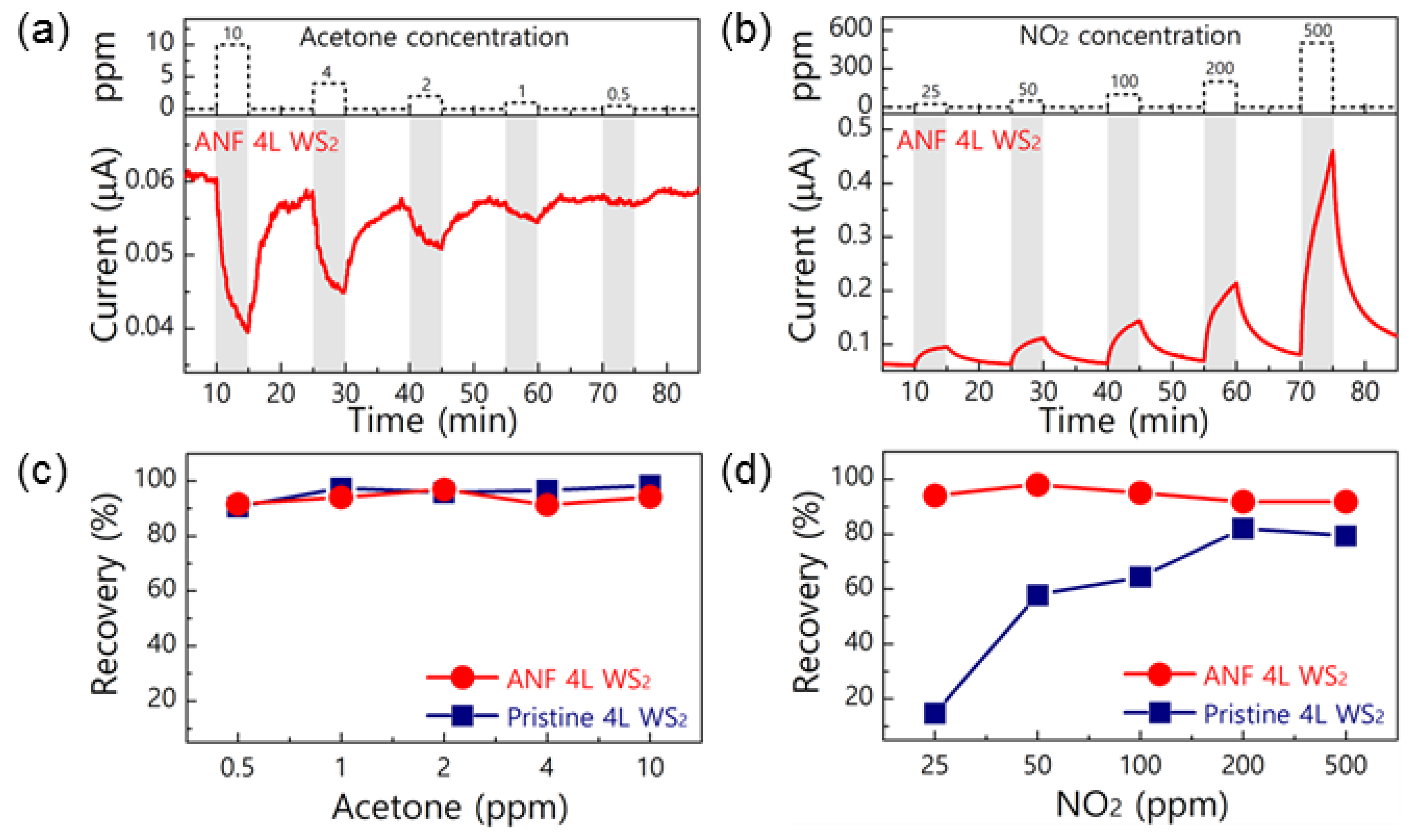
Figure 9.
(a) Top and cross-sectional schematics of SnS2. (b) Zoomed-in HRTEM figure indicating that the interlayer spacing for hexagonal SnS2 is 0.587 nm. (c) Dynamic sensing performance of 2D SnS2 flakes toward NO2 gas at concentrations ranging from 0.6–10 ppm under the operation temperature of 120 °C. (d) Measured cross-talk of 2D SnS2 flakes toward H2 (1%), CH4 (10%), CO2 (10%), H2S (56 ppm) and NO2 (10 ppm) (Reproduced with permission of [52]. Copyright American Chemical Society, 2015.).

Figure 10.
(a) The time-dependent current response of TaS2 sensors at different concentrations of NO. (b) Plot of the detection sensitivity versus the concentration of NO. Standard error was obtained by testing five devices from the same batch of TaS2 film (c) Current profile of device under continuous exposure of NO. The dotted red lines in (c) show the concentration profile of exposed NO. (d) Plot of the current response versus the integrated toxic load. (Reproduced with permission of [53]. Copyright He et al. TaS2 nanosheet-based room-temperature dosage meter for nitric oxide, AIP Materials, 2, 092506, 2014.).
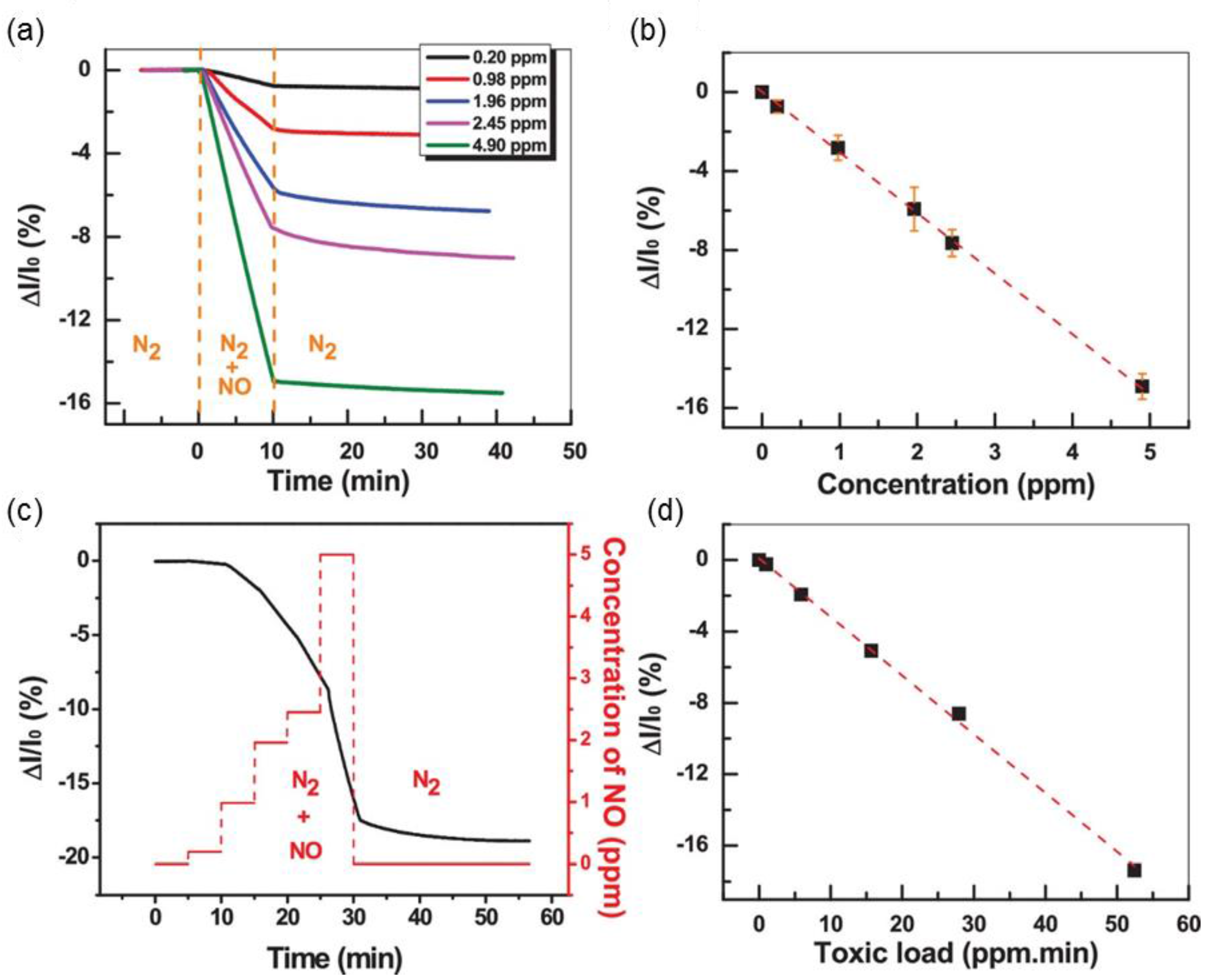
Figure 11.
(a) SEM image of SnO2-SnS2-0.5. (b) Schematic illustration of SnO2-SnS2 contacts. (c) The inset shows the response of the obtained samples to a NH3 with 100 ppm. Repetitive dynamic response-recovery curves of SnO2-SnS2-0.5, SnO2-SnS2-1 and SnO2-SnS2-2. (d) The response-recovery curves of SnO2-SnS2-1 to NH3 in the concentration range from 10–500 ppm. The inset shows the response as a function of NH3 concentration (Reproduced with permission of [57]. Copyright American Chemical Society, 2015.).
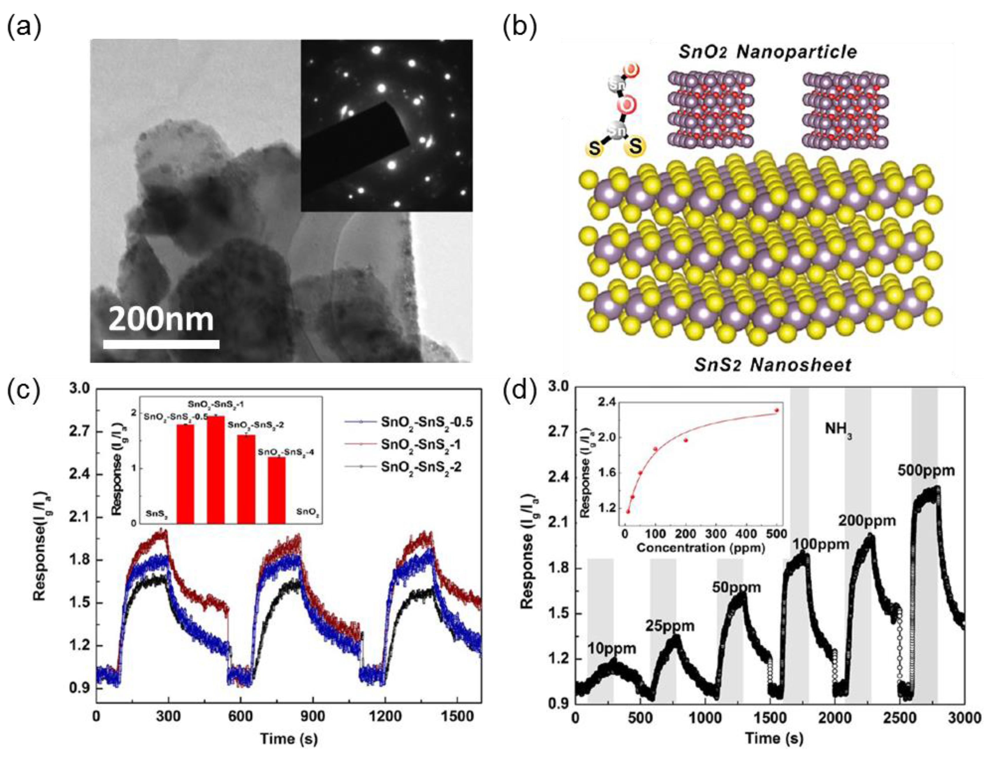
Figure 12.
(a) Three basic factors controlling semiconductor gas sensors. (b) STEM- annular dark-field (ADF) image of a MoS2 grain boundary with its common dislocations highlighted and close-ups of the regions highlighted (Reproduced with permission of [69]. Copyright Nature Publishing Group, 2013.).

© 2017 by the authors. Licensee MDPI, Basel, Switzerland. This article is an open access article distributed under the terms and conditions of the Creative Commons Attribution (CC BY) license (http://creativecommons.org/licenses/by/4.0/).
Share and Cite
MDPI and ACS Style
Kim, T.H.; Kim, Y.H.; Park, S.Y.; Kim, S.Y.; Jang, H.W. Two-Dimensional Transition Metal Disulfides for Chemoresistive Gas Sensing: Perspective and Challenges. Chemosensors 2017, 5, 15. https://doi.org/10.3390/chemosensors5020015
AMA Style
Kim TH, Kim YH, Park SY, Kim SY, Jang HW. Two-Dimensional Transition Metal Disulfides for Chemoresistive Gas Sensing: Perspective and Challenges. Chemosensors. 2017; 5(2):15. https://doi.org/10.3390/chemosensors5020015
Chicago/Turabian StyleKim, Tae Hoon, Yeon Hoo Kim, Seo Yun Park, Soo Young Kim, and Ho Won Jang. 2017. "Two-Dimensional Transition Metal Disulfides for Chemoresistive Gas Sensing: Perspective and Challenges" Chemosensors 5, no. 2: 15. https://doi.org/10.3390/chemosensors5020015
Note that from the first issue of 2016, this journal uses article numbers instead of page numbers. See further details here.