Detection and Digital Resolution Counting of Nanoparticles with Optical Resonators and Applications in Biosensing

 ,
, 
Abstract
:1. Introduction
2. Non-Imaging Single Nanoparticle Sensing Methods Materials and Methods
2.1. Photonic Crystal Cavities
2.1.1. PC Nanobeam Cavities
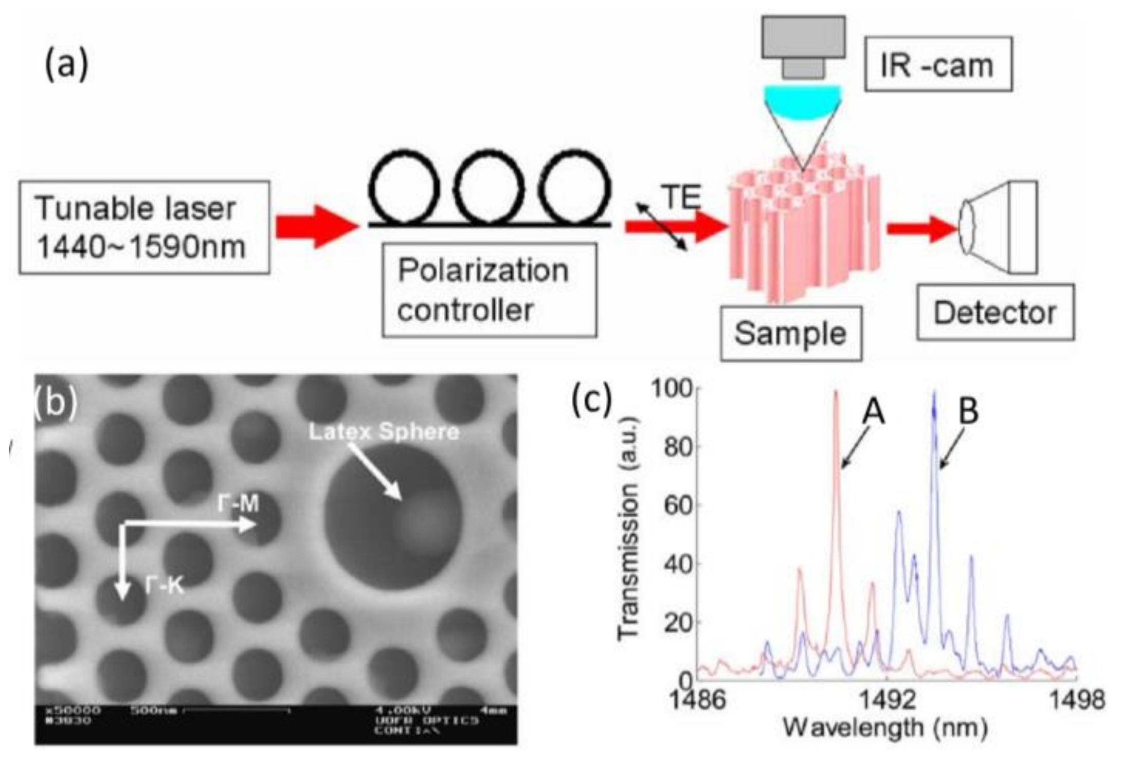
2.1.2. PC Cavities
Point-Like Defects
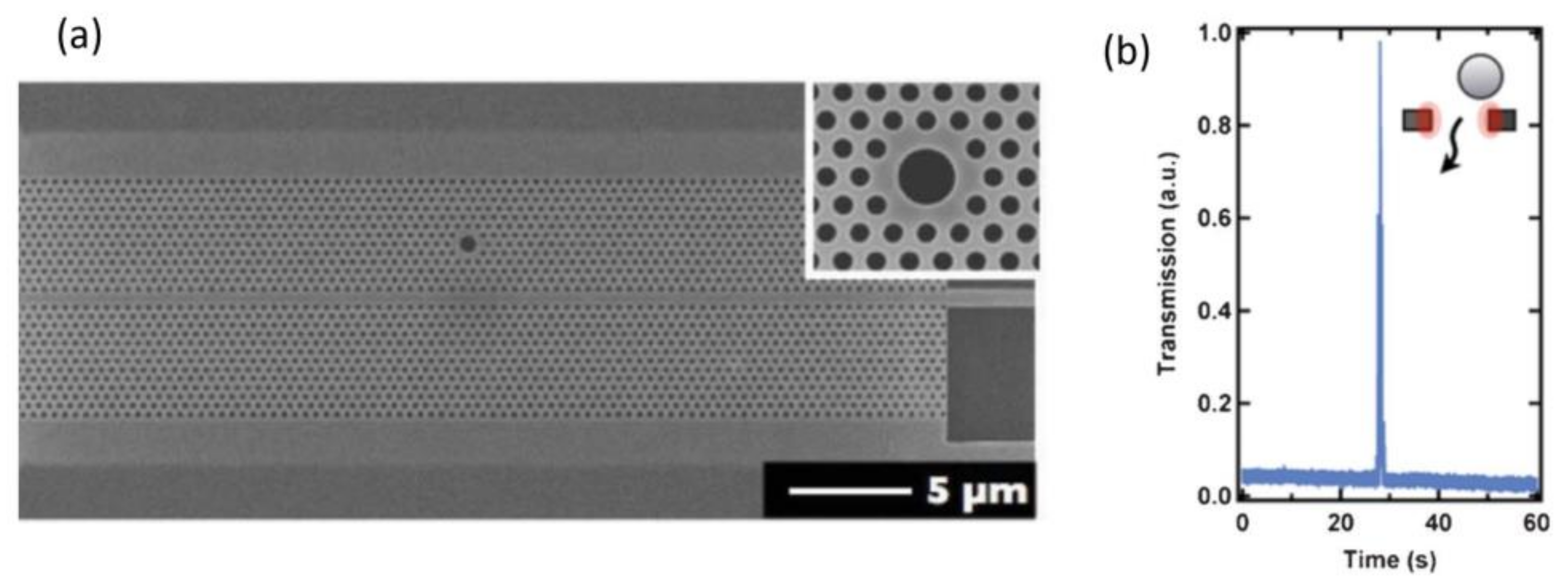
Waveguide Defect
Slotted Waveguide Defect
2.2. Whispering Gallery Mode Sensors
2.2.1. WSG Sensing Principle
WSG Sensor Frequency Shift
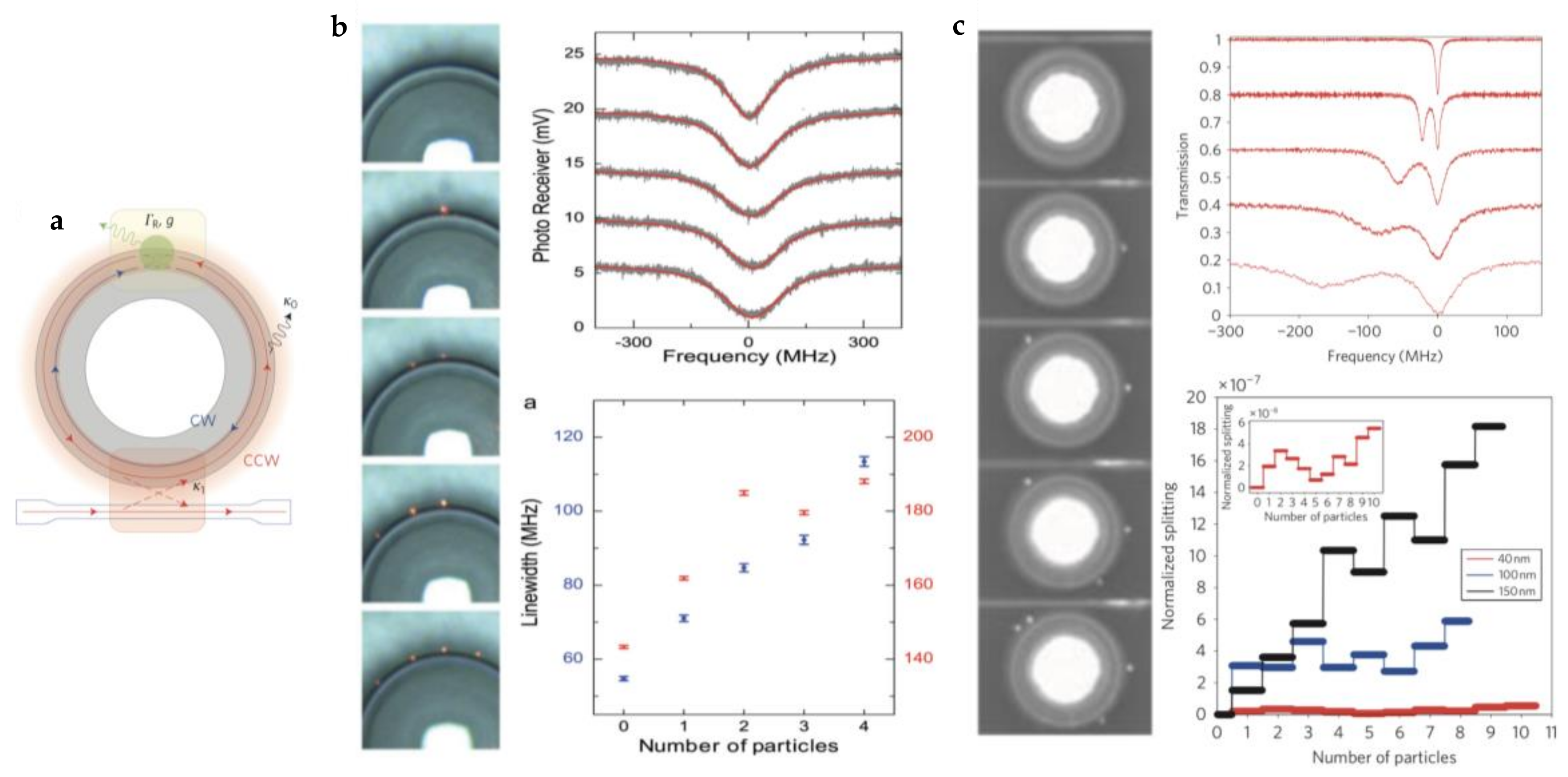
WSG Mode Splitting
WSG Sensing by Line Broadening
3. Imaging Methods
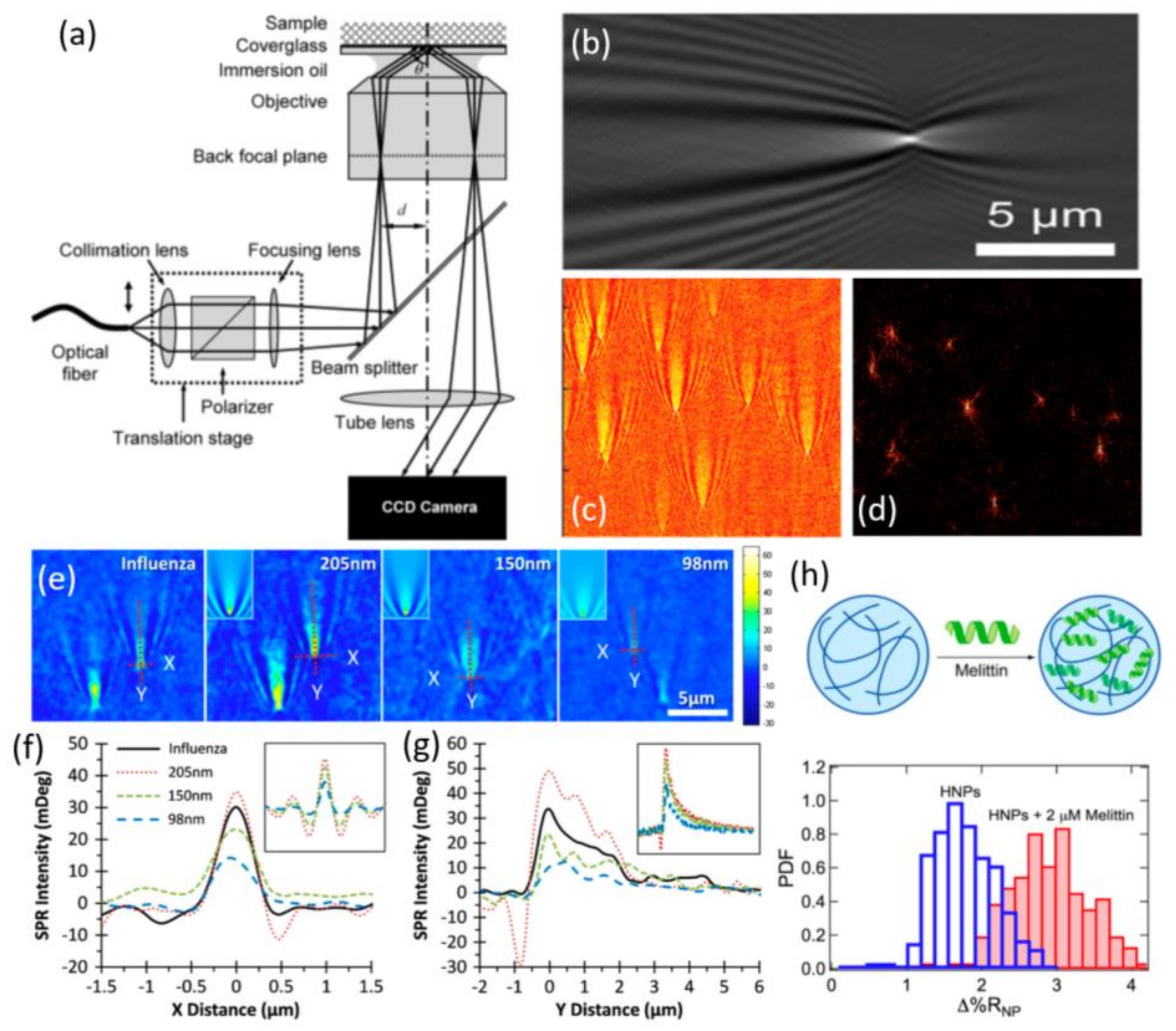
3.1. Surface Plasmon Resonance Imaging Microscopy
3.1.1. Imaging Principle
3.1.2. Spatial Resolution and Image Reconstruction
3.1.3. Nanoparticle Sizing and Specification
3.2. Interferometric Reflectance Imaging Sensor
3.2.1. Low Magnification IRIS
3.2.2. High Magnification IRIS
3.2.3. Evolution of the IRIS System
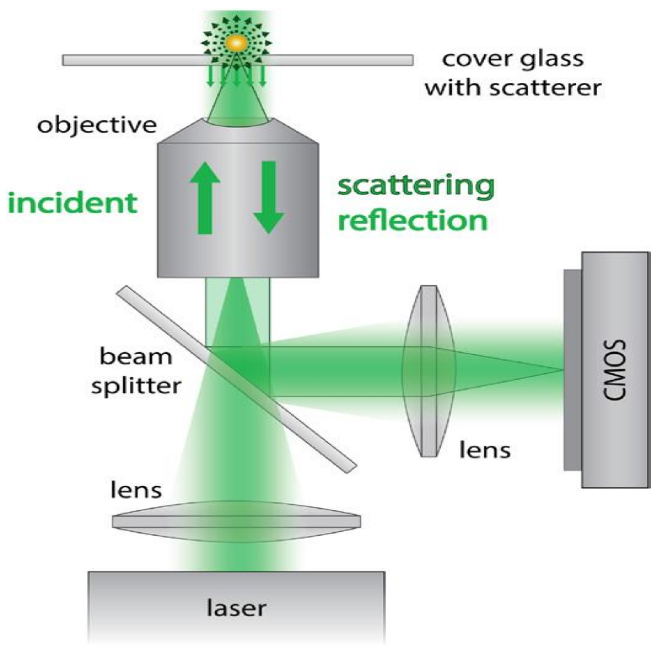
3.3. Interferometric Scattering Microscopy
3.4. Dark-Field Microscopy
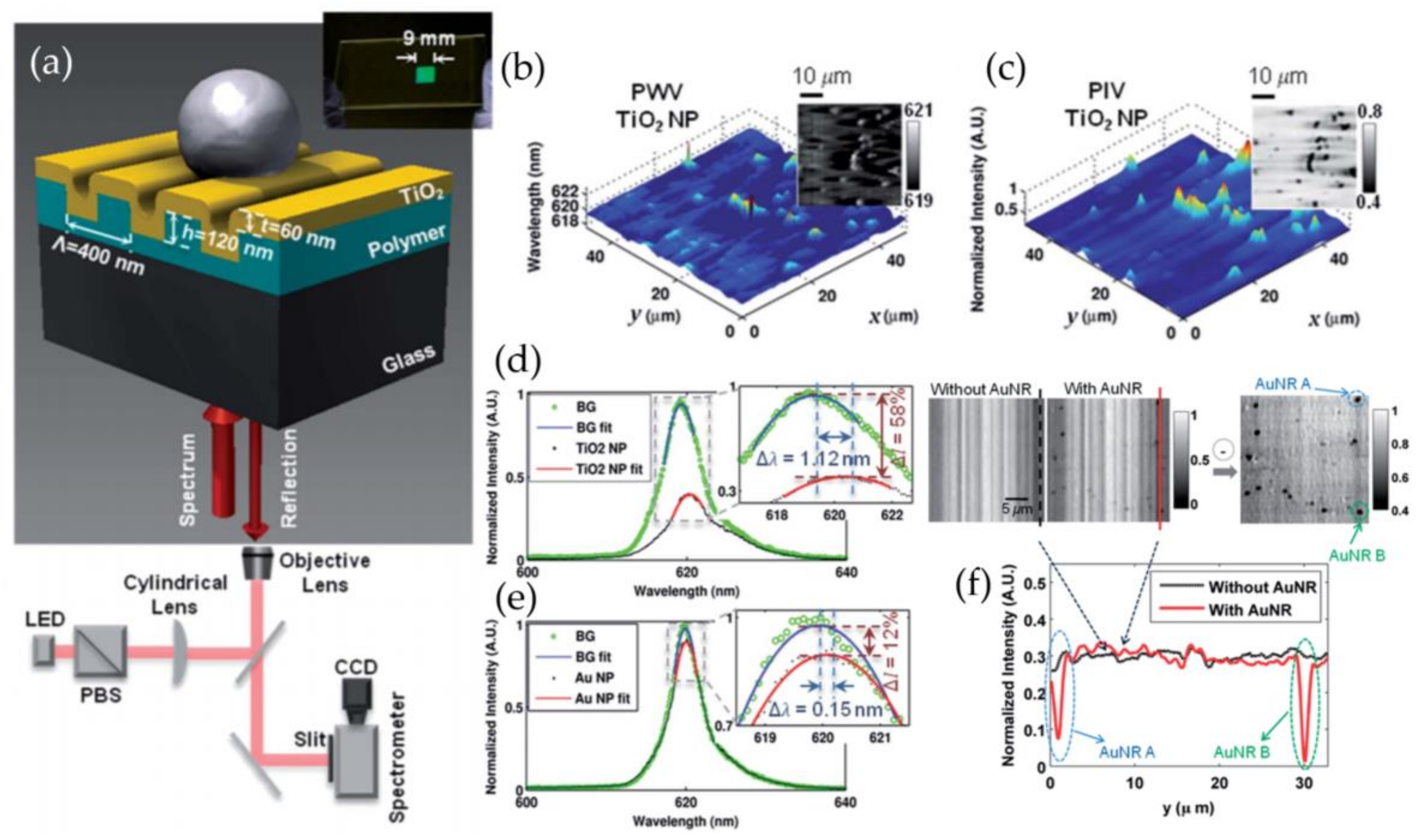
3.5. Photonic Crystal Enhanced Microscopy
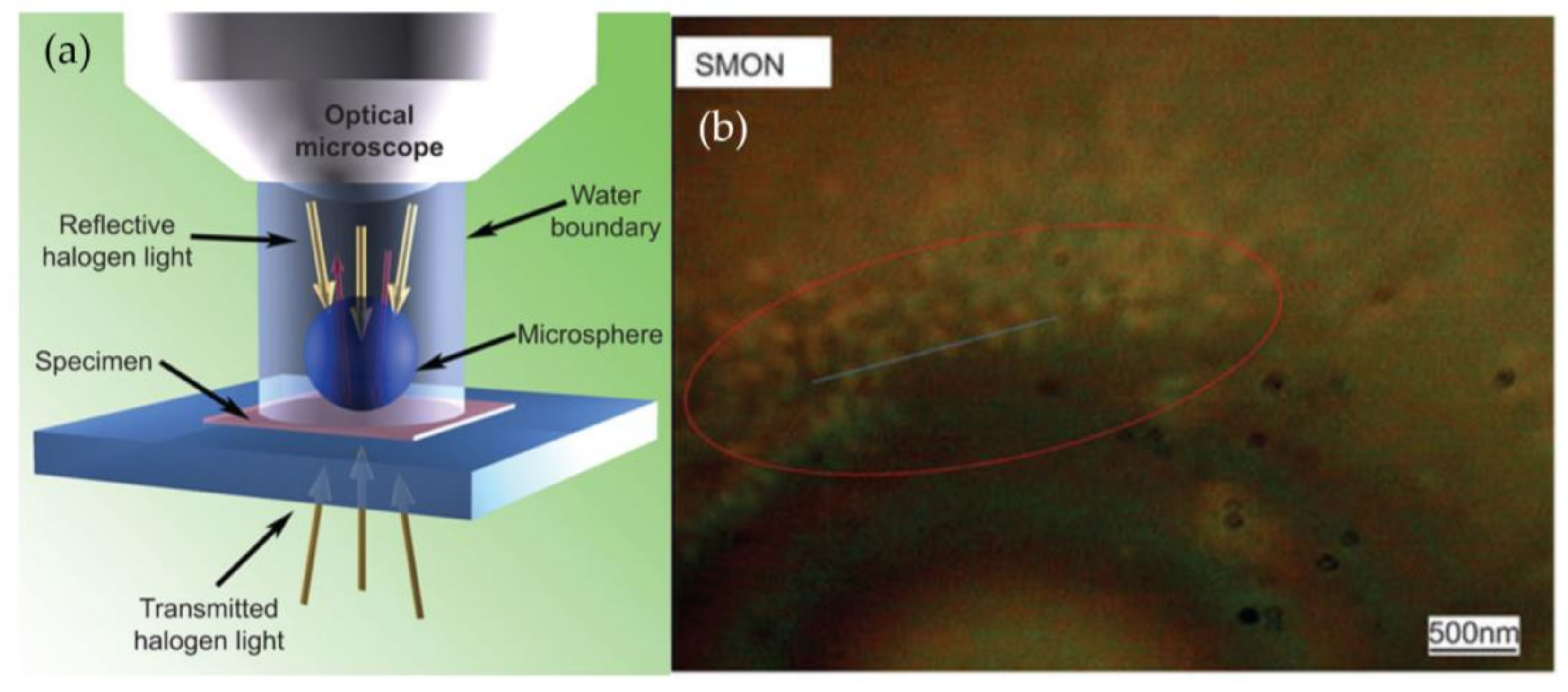
3.6. Super Resolution Microscopy with Microspheres (SMON)
4. Conclusions
Acknowledgments
Conflicts of Interest
References
- Sydor, A.M.; Czymmek, K.J.; Puchner, E.M.; Mennella, V. Super-resolution microscopy: From single molecules to supramolecular assemblies. Trends Cell Biol. 2015, 25, 730–748. [Google Scholar] [CrossRef] [PubMed]
- Stone, M.B.; Shelby, S.A.; Veatch, S.L. Super-resolution microscopy: Shedding light on the cellular plasma membrane. Chem. Rev. 2017, 117, 7457–7477. [Google Scholar] [CrossRef] [PubMed]
- Huang, B. Super-resolution optical microscopy: Multiple choices. Curr. Opin. Chem. Biol. 2010, 14, 10–14. [Google Scholar] [CrossRef] [PubMed]
- Thurn, K.T.; Paunesku, T.; Wu, A.; Brown, E.M.; Lai, B.; Vogt, S.; Maser, J.; Aslam, M.; Dravid, V.; Bergan, R.; et al. Labeling TiO2 nanoparticles with dyes for optical fluorescence microscopy and determination of TiO2-DNA nanoconjugate stability. Small 2009, 5, 1318–1325. [Google Scholar] [CrossRef] [PubMed]
- Ishii, D.; Kinbara, K.; Ishida, Y.; Ishii, N.; Okochi, M.; Yohda, M.; Aida, T. Chaperonin-mediated stabilization and ATP-triggered release of semiconductor nanoparticles. Nature 2003, 423, 628–632. [Google Scholar] [CrossRef] [PubMed]
- Sperling, R.A.; Gil, P.R.; Zhang, F.; Marco, Z.; Parak, W.J. Biological applications of gold nanoparticles. Chem. Soc. Rev. 2008, 37, 1896–1908. [Google Scholar] [CrossRef] [PubMed]
- Jaiswal, A.; Tian, L.M.; Tadepalli, S.; Liu, K.K.; Fei, M.; Farrell, M.E.; Pellegrino, P.M.; Singamaneni, S. Plasmonic Nanorattles with Intrinsic Electromagnetic Hot-Spots for Surface Enhanced Raman Scattering. Small 2014, 10, 4287–4292. [Google Scholar] [CrossRef] [PubMed]
- McFarland, A.D.; Van Duyne, R.P. Single silver nanoparticles as real-time optical sensors with zeptomole sensitivity. Nano Lett. 2003, 3, 1057–1062. [Google Scholar] [CrossRef]
- Ringe, E.; Sharma, B.; Henry, A.I.; Marks, L.D.; Van Duyne, R.P. Single nanoparticle plasmonics. Phys. Chem. Chem. Phys. 2013, 15, 4110–4129. [Google Scholar] [CrossRef] [PubMed]
- Winter, P.M.; Morawski, A.M.; Caruthers, S.D.; Fuhrhop, R.W.; Zhang, H.; Williams, T.A.; Allen, J.S.; Lacy, E.K.; Robertson, J.D.; Lanza, G.M.; et al. Molecular imaging of angiogenesis in early-stage atherosclerosis with αvβ3-Integrin−targeted nanoparticles. Circulation 2003, 108, 2270–2274. [Google Scholar] [CrossRef] [PubMed]
- Singamaneni, S.; Bliznyuk, V.N.; Binek, C.; Tsymbal, E.Y. Magnetic nanoparticles: Recent advances in synthesis, self-assembly and applications. J. Mater. Chem. 2011, 21, 16819–16845. [Google Scholar] [CrossRef]
- Miller, M.F.; Masters, B.P.; Lundstrom, M.E. Method and Apparatus for Detection of Analyte Using a Flexural Plate Wave Device and Magnetic Particles. U.S. Patent 7,300,631, 27 November 2007. [Google Scholar]
- Wang, Y.; Chen, H.; Dong, S.; Wang, E. Surface-enhanced Raman scattering of silver-gold bimetallic nanostructures with hollow interiors. J. Chem. Phys. 2006, 125, 44710. [Google Scholar] [CrossRef] [PubMed]
- Cognet, L.; Tardin, C.; Boyer, D.; Choquet, D.; Tamarat, P.; Lounis, B. Single metallic nanoparticle imaging for protein detection in cells. Proc. Natl. Acad. Sci. USA 2003, 100, 11350–11355. [Google Scholar] [CrossRef] [PubMed]
- Lee, J.; Shen, W.; Payer, K.; Burg, T.P.; Manalis, S.R. Toward attogram mass measurements in solution with suspended nanochannel resonators. Nano Lett. 2010, 10, 2537–2542. [Google Scholar] [CrossRef] [PubMed] [Green Version]
- Michel, F.M.; Ehm, L.; Antao, S.M.; Lee, P.L.; Chupas, P.J.; Liu, G.; Strongin, D.R.; Schoonen, M.A.A.; Phillips, B.L.; Parise, J.B. The structure of ferrihydrite, a nanocrystalline material. Science 2007, 316, 1726–1729. [Google Scholar] [CrossRef] [PubMed]
- Lu, T.; Lee, H.; Chen, T.; Herchak, S.; Kim, J.H.; Fraser, S.E.; Flagan, R.C.; Vahala, K. High sensitivity nanoparticle detection using optical microcavities. Proc. Natl. Acad. Sci. USA 2011, 108, 5976–5979. [Google Scholar] [CrossRef] [PubMed]
- Gupta, A.; Akin, D.; Bashir, R. Single virus particle mass detection using microresonators with nanoscale thickness. Appl. Phys. Lett. 2004, 84, 1976–1978. [Google Scholar] [CrossRef]
- Juan, M.L.; Gordon, R.; Pang, Y.; Eftekhari, F.; Quidant, R. Self-induced back-action optical trapping of dielectric nanoparticles. Nat. Phys. 2009, 5, 915–919. [Google Scholar] [CrossRef]
- Kotnala, A.; DePaoli, D.; Gordon, R. Sensing nanoparticles using a double nanohole optical trap. Lab Chip 2013, 13, 4142–4146. [Google Scholar] [CrossRef] [PubMed]
- Zhu, J.; Ozdemir, S.K.; Xiao, Y.-F.; Li, L.; He, L.; Chen, D.-R.; Yang, L. On-chip single nanoparticle detection and sizing by mode splitting in an ultrahigh-Q microresonator. Nat. Photonics 2010, 4, 46–49. [Google Scholar] [CrossRef]
- Nie, S.; Emory, S.R. Probing single molecules and single nanoparticles by surface-enhanced Raman scattering. Science 1997, 275, 1102–1106. [Google Scholar] [CrossRef] [PubMed]
- Zhang, W.H.; Huang, L.N.; Santschi, C.; Martin, O.J.F. Trapping and sensing 10 nm metal nanoparticles using plasmonic dipole antennas. Nano Lett. 2010, 10, 1006–1011. [Google Scholar] [CrossRef] [PubMed]
- Wang, S.P.; Shan, X.N.; Patel, U.; Huang, X.P.; Lu, J.; Li, J.H.; Tao, N.J. Label-free imaging, detection, and mass measurement of single viruses by surface plasmon resonance. Proc. Natl. Acad. Sci. USA 2010, 107, 16028–16032. [Google Scholar] [CrossRef] [PubMed]
- Cunningham, B.; Lin, B.; Qiu, J.; Li, P.; Pepper, J.; Hugh, B. A plastic colorimetric resonant optical biosensor for multiparallel detection of label-free biochemical interactions. Sens. Actuator B Chem. 2002, 85, 219–226. [Google Scholar] [CrossRef]
- Cunningham, B.; Li, P.; Lin, B.; Pepper, J. Colorimetric resonant reflection as a direct biochemical assay technique. Sens. Actuator B Chem. 2002, 81, 316–328. [Google Scholar] [CrossRef]
- Cunningham, B.T.; Li, P.; Schulz, S.; Lin, B.; Baird, C.; Gerstenmaier, J.; Genick, C.; Wang, F.; Fine, E.; Laing, L. Label-free assays on the BIND system. J. Biomol. Screen. 2004, 9, 481–490. [Google Scholar] [CrossRef] [PubMed]
- Ganesh, N.; Block, I.D.; Cunningham, B.T. Near ultraviolet-wavelength photonic-crystal biosensor with enhanced surface-to-bulk sensitivity ratio. Appl. Phys. Lett. 2006, 89, 023901. [Google Scholar] [CrossRef]
- Grepstad, J.O.; Kaspar, P.; Solgaard, O.; Johansen, I.R.; Sudbo, A.S. Photonic-crystal membranes for optical detection of single nano-particles, designed for biosensor application. Opt. Express 2012, 20, 7954–7965. [Google Scholar] [CrossRef] [PubMed]
- Vedula, R.; Daaboul, G.; Reddington, A.; Ozkumur, E.; Bergstein, D.A.; Unlu, M.S. Self-referencing substrates for optical interferometric biosensors. J. Mod. Opt. 2010, 57, 1564–1569. [Google Scholar] [CrossRef]
- Daaboul, G.G.; Yurt, A.; Zhang, X.; Hwang, G.M.; Goldberg, B.B.; Unlu, M.S. High-throughput detection and sizing of individual low-index nanoparticles and viruses for pathogen identification. Nano Lett. 2010, 10, 4727–4731. [Google Scholar] [CrossRef] [PubMed]
- Monroe, M.R.; Daaboul, G.G.; Tuysuzoglu, A.; Lopez, C.A.; Little, F.F.; Unlu, M.S. Single nanoparticle detection for multiplexed protein diagnostics with attomolar sensitivity in serum and unprocessed whole blood. Anal. Chem. 2013, 85, 3698–3706. [Google Scholar] [CrossRef] [PubMed]
- Person, S.; Deutsch, B.; Mitra, A.; Novotny, L. Material-specific detection and classification of single nanoparticles. Nano Lett. 2011, 11, 257–261. [Google Scholar] [CrossRef] [PubMed]
- Wong, C.L.; Chen, G.C.K.; Ng, B.K.; Agarwal, S.; Fanani, N.; Lin, Z.P.; Vasudevan, S.; Chen, P. Photothermal imaging of nanoparticles beyond the diffraction limit. Opt. Eng. 2011, 50, 073201. [Google Scholar] [CrossRef]
- Kim, S.-M.; Zhang, W.; Cunningham, B.T. Photonic crystals with SiO2–Ag “post-cap” nanostructure coatings for surface enhanced Raman spectroscopy. Appl. Phys. Lett. 2008, 93, 143112. [Google Scholar] [CrossRef]
- Kim, S.-m.; Zhang, W.; Cunningham, B.T. Coupling discrete metal nanoparticles to photonic crystal surface resonant modes and application to Raman spectroscopy. Opt. Express 2010, 18, 4300–4309. [Google Scholar] [CrossRef] [PubMed]
- Lin, S.; Zhu, W.; Jin, Y.; Crozier, K.B. Surface-enhanced Raman scattering with Ag nanoparticles optically trapped by a photonic crystal cavity. Nano Lett. 2013, 13, 559–563. [Google Scholar] [CrossRef] [PubMed]
- Liu, J.-N.; Huang, Q.; Liu, K.-K.; Singamaneni, S.; Cunningham, B.T. Nanoantenna-microcavity hybrids with highly cooperative plasmonic-photonic coupling. Nano Lett. 2017, 17, 7569–7577. [Google Scholar] [CrossRef] [PubMed]
- Mora, J.; Chunyk, A.G.; Dysinger, M.; Purushothama, S.; Ricks, C.; Otsterlund, K.; Theobald, V. Next generation ligand binding assays-review of emerging technologies’ capabilities to enhance throughput and multiplexing. AAPS J. 2014, 16, 1175–1184. [Google Scholar] [CrossRef] [PubMed]
- Fischer, S.K.; Joyce, A.; Spengler, M.; Yang, T.Y.; Zhuang, Y.; Fjording, M.S.; Mikulskis, A. Emerging technologies to increase ligand binding assay sensitivity. AAPS J. 2015, 17, 93–101. [Google Scholar] [CrossRef] [PubMed]
- Rissin, D.M.; Kan, C.W.; Campbell, T.G.; Howes, S.C.; Fournier, D.R.; Song, L.; Piech, T.; Patel, P.P.; Chang, L.; Rivnak, A.J.; et al. Single-molecule enzyme-linked immunosorbent assay detects serum proteins at subfemtomolar concentrations. Nat. Biotechnol. 2010, 28, 595–599. [Google Scholar] [CrossRef] [PubMed]
- Petryayeva, E.; Algar, W.R.; Medintz, I.L. Quantum dots in bioanalysis: A review of applications across various platforms for fluorescence spectroscopy and imaging. Appl. Spectrosc. 2013, 67, 215–252. [Google Scholar] [CrossRef] [PubMed]
- Rosenthal, S.J.; Chang, J.C.; Kovtun, O.; McBride, J.R.; Tomlinson, I.D. Biocompatible quantum dots for biological applications. Chem. Biol. 2011, 18, 10–24. [Google Scholar] [CrossRef] [PubMed]
- Medintz, I.L.; Uyeda, H.T.; Goldman, E.R.; Mattoussi, H. Quantum dot bioconjugates for imaging, labelling and sensing. Nat. Mater. 2005, 4, 435–446. [Google Scholar] [CrossRef] [PubMed]
- Lane, L.A.; Qian, X.M.; Nie, S.M. SERS nanoparticles in medicine: From label-free detection to spectroscopic tagging. Chem. Rev. 2015, 115, 10489–10529. [Google Scholar] [CrossRef] [PubMed]
- Bettegowda, C.; Sausen, M.; Leary, R.; Kinde, I.; Agrawal, N.; Bartlett, B.; Wang, H.; Luber, B.; Kinzler, K.; Vogelstein, B.; et al. Detection of circulating tumor DNA in early and late stage human malignancies. Cancer Res. 2014, 74, 5606. [Google Scholar] [CrossRef]
- Diaz, L.A.; Bardelli, A. Liquid biopsies: Genotyping circulating tumor DNA. J. Clin. Oncol. 2014, 32, 579–586. [Google Scholar] [CrossRef] [PubMed]
- Garzon, R.; Calin, G.A.; Croce, C.M. MicroRNAs in Cancer. Annu. Rev. Med. 2009, 60, 167–179. [Google Scholar] [CrossRef] [PubMed]
- Hunt, E.A.; Goulding, A.M.; Deo, S.K. Direct detection and quantification of microRNAs. Anal. Biochem. 2009, 387, 1–12. [Google Scholar] [CrossRef] [PubMed] [Green Version]
- Li, W.; Ruan, K.C. MicroRNA detection by microarray. Anal. Bioanal. Chem. 2009, 394, 1117–1124. [Google Scholar] [CrossRef] [PubMed]
- Lalanne, P. Effective medium theory applied to photonic crystals composed of cubic or square cylinders. Appl. Opt. 1996, 35, 5369–5380. [Google Scholar] [CrossRef] [PubMed]
- Conteduca, D.; Dell’Olio, F.; Krauss, T.F.; Ciminelli, C. Photonic and plasmonic nanotweezing of nano- and microscale particles. Appl. Spectrosc. 2017, 71, 367–390. [Google Scholar] [CrossRef] [PubMed]
- Zhi, Y.; Yu, X.C.; Gong, Q.; Yang, L.; Xiao, Y.F. Single nanoparticle detection using optical microcavities. Adv. Mater. 2017, 29, 1604920. [Google Scholar] [CrossRef] [PubMed]
- Vaiano, P.; Carotenuto, B.; Pisco, M.; Ricciardi, A.; Quero, G.; Consales, M.; Crescitelli, A.; Esposito, E.; Cusano, A. Lab on Fiber Technology for biological sensing applications. Laser Photonics Rev. 2016, 10, 922–961. [Google Scholar] [CrossRef]
- Lin, T.; Zhang, X.; Zhou, G.; Siong, C.F.; Deng, J. Design of an ultra-compact slotted photonic crystal nanobeam cavity for biosensing. J. Opt. Soc. Am. B 2015, 32, 1788–1791. [Google Scholar] [CrossRef]
- Baker, J.E.; Sriram, R.; Miller, B.L. Two-dimensional photonic crystals for sensitive microscale chemical and biochemical sensing. Lab Chip 2015, 15, 971–990. [Google Scholar] [CrossRef] [PubMed]
- Scullion, M.G.; Krauss, T.F.; Di-Falco, A. Slotted photonic crystal sensors. Sensors 2013, 13, 3675–3710. [Google Scholar] [CrossRef] [PubMed] [Green Version]
- Yoshie, T.; Tang, L.; Su, S.-Y. Optical microcavity: Sensing down to single molecules and atoms. Sensors 2011, 11, 1972–1991. [Google Scholar] [CrossRef] [PubMed]
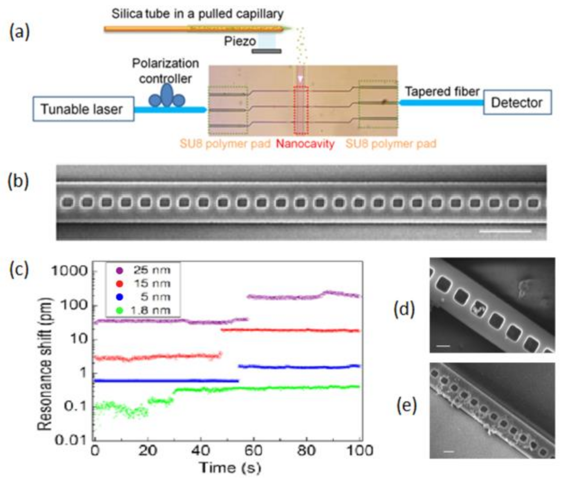
- Liang, F.; Quan, Q. Detecting single gold nanoparticles (1.8 nm) with ultrahigh-Q air-mode photonic crystal nanobeam cavities. ACS Photonics 2015, 2, 1692–1697. [Google Scholar] [CrossRef]
- Quan, Q.; Deotare, P.B.; Loncar, M. Photonic crystal nanobeam cavity strongly coupled to the feeding waveguide. Appl. Phys. Lett. 2010, 96, 203102. [Google Scholar] [CrossRef]
- Mandal, S.; Serey, X.; Erickson, D. Nanomanipulation using silicon photonic crystal resonators. Nano Lett. 2010, 10, 99–104. [Google Scholar] [CrossRef] [PubMed]
- Liang, F.; Clarke, N.; Patel, P.; Loncar, M.; Quan, Q. Scalable photonic crystal chips for high sensitivity protein detection. Opt. Express 2013, 21, 32306–32312. [Google Scholar] [CrossRef] [PubMed]
- Renaut, C.; Dellinger, J.; Cluzel, B.; Honegger, T.; Peyrade, D.; Picard, E.; de Fornel, F.; Hadji, E. Assembly of microparticles by optical trapping with a photonic crystal nanocavity. Appl. Phys. Lett. 2012, 100, 101103. [Google Scholar] [CrossRef]
- Wang, C.; Quan, Q.; Kita, S.; Li, Y.; Lončar, M. Single-nanoparticle detection with slot-mode photonic crystal cavities. Appl. Phys. Lett. 2015, 106, 261105. [Google Scholar] [CrossRef]
- Lin, S.; Crozier, K.B. Trapping-assisted sensing of particles and proteins using on-chip optical microcavities. ACS Nano 2013, 7, 1725–1730. [Google Scholar] [CrossRef] [PubMed]
- Chen, Y.F.; Serey, X.; Sarkar, R.; Chen, P.; Erickson, D. Controlled photonic manipulation of proteins and other nanomaterials. Nano Lett. 2012, 12, 1633–1637. [Google Scholar] [CrossRef] [PubMed]
- Baker, S.E.; Pocha, M.D.; Chang, A.S.P.; Sirbuly, D.J.; Cabrini, S.; Dhuey, S.D.; Bond, T.C.; Létant, S.E. Detection of bio-organism simulants using random binding on a defect-free photonic crystal. Appl. Phys. Lett. 2010, 97, 113701. [Google Scholar] [CrossRef]
- Dharanipathy, U.P.; Houdré, R. Numerical modelling of optical trapping in hollow photonic crystal cavities. Opt. Quantum Electron. 2012, 44, 161–167. [Google Scholar] [CrossRef]
- Intonti, F.; Vignolini, S.; Riboli, F.; Zani, M.; Wiersma, D.S.; Balet, L.; Li, L.H.; Francardi, M.; Gerardino, A.; Fiore, A.; et al. Tuning of photonic crystal cavities by controlled removal of locally infiltrated water. Appl. Phys. Lett. 2009, 95, 173112. [Google Scholar] [CrossRef]
- Lee, M.R.; Fauchet, P.M. Nanoscale microcavity sensor for single particle detection. Opt. Lett. 2007, 32, 3284–3286. [Google Scholar] [CrossRef] [PubMed]
- Lee, M.; Fauchet, P.M. Two-dimensional silicon photonic crystal based biosensing platform for protein detection. Opt. Express 2007, 15, 4530–4535. [Google Scholar] [CrossRef]
- Zlatanovic, S.; Mirkarimi, L.W.; Sigalas, M.M.; Bynum, M.A.; Chow, E.; Robotti, K.M.; Burr, G.W.; Esener, S.; Grot, A. Photonic crystal microcavity sensor for ultracompact monitoring of reaction kinetics and protein concentration. Sens. Actuator B Chem. 2009, 141, 13–19. [Google Scholar] [CrossRef]
- Kita, S.; Nozaki, K.; Baba, T. Refractive index sensing utilizing a cw photonic crystal nanolaser and its array configuration. Opt. Express 2008, 16, 8174–8180. [Google Scholar] [CrossRef] [PubMed]
- Leest, T.V.; Caro, J. Cavity-enhanced optical trapping of bacteria using a silicon photonic crystal. Lab Chip 2013, 13, 4358–4365. [Google Scholar] [CrossRef] [PubMed]
- Chakravarty, S.; Topol’ančik, J.; Bhattacharya, P.; Chakrabarti, S.; Kang, Y.; Meyerhoff, M.E. Ion detection with photonic crystal microcavities. Opt. Lett. 2005, 30, 2578–2580. [Google Scholar] [CrossRef] [PubMed]
- Asano, T.; Ochi, Y.; Takahashi, Y.; Kishimoto, K.; Noda, S. Photonic crystal nanocavity with a Q factor exceeding eleven million. Opt. Express 2017, 25, 1769–1777. [Google Scholar] [CrossRef] [PubMed]
- Liu, Y.; Salemink, H.W.M. Photonic crystal-based all-optical on-chip sensor. Opt. Express 2012, 20, 19912–19920. [Google Scholar] [CrossRef] [PubMed]
- Shambat, G.; Kothapalli, S.R.; Khurana, A.; Provine, J.; Sarmiento, T.; Cheng, K.; Cheng, Z.; Harris, J.; Daldrup-Link, H.; Gambhir, S.S.; et al. A photonic crystal cavity-optical fiber tip nanoparticle sensor for biomedical applications. Appl. Phys. Lett. 2012, 100, 213702. [Google Scholar] [CrossRef]
- Shambat, G.; Provine, J.; Rivoire, K.; Sarmiento, T.; Harris, J.; Vučković, J. Optical fiber tips functionalized with semiconductor photonic crystal cavities. Appl. Phys. Lett. 2011, 99, 191102. [Google Scholar] [CrossRef]
- Lončar, M.; Nedeljković, D.; Doll, T.; Vučković, J.; Scherer, A.; Pearsall, T.P. Waveguiding in planar photonic crystals. Appl. Phys. Lett. 2000, 77, 1937–1939. [Google Scholar] [CrossRef]
- Olivier, S.; Rattier, M.; Benisty, H.; Weisbuch, C.; Smith, C.J.M.; De-La-Rue, R.M.; Krauss, T.F.; Oesterle, U.; Houdré, R. Mini-stopbands of a one-dimensional system: The channel waveguide in a two-dimensional photonic crystal. Phys. Rev. B 2001, 63, 113311. [Google Scholar] [CrossRef]
- Notomi, M.; Shinya, A.; Mitsugi, S.; Kuramochi, E.; Ryu, H.Y. Waveguides, resonators and their coupled elements in photonic crystal slabs. Opt. Express 2004, 12, 1551–1561. [Google Scholar] [CrossRef]
- Inoshita, K.; Baba, T. Lasing at bend, branch and intersection of photonic crystal waveguides. Electron. Lett. 2003, 39, 844–846. [Google Scholar] [CrossRef]
- Song, B.S.; Noda, S.; Asano, T.; Akahane, Y. Ultra-high-Q photonic double-heterostructure nanocavity. Nat. Mater. 2005, 4, 207–210. [Google Scholar] [CrossRef]
- Descharmes, N.; Dharanipathy, U.P.; Diao, Z.; Tonin, M.; Houdré, R. Observation of backaction and self-induced trapping in a planar hollow photonic crystal cavity. Phys. Rev. Lett. 2013, 110, 123601. [Google Scholar] [CrossRef] [PubMed]
- Descharmes, N.; Dharanipathy, U.P.; Diao, Z.; Tonin, M.; Houdre, R. Single particle detection, manipulation and analysis with resonant optical trapping in photonic crystals. Lab Chip 2013, 13, 3268–3274. [Google Scholar] [CrossRef] [PubMed]
- Baker, J.E.; Sriram, R.; Miller, B.L. Recognition-mediated particle detection under microfluidic flow with waveguide-coupled 2D photonic crystals: Towards integrated photonic virus detectors. Lab Chip 2017, 17, 1570–1577. [Google Scholar] [CrossRef] [PubMed]
- Pal, S.; Yadav, A.R.; Lifson, M.A.; Baker, J.E.; Fauchet, P.M.; Miller, B.L. Selective virus detection in complex sample matrices with photonic crystal optical cavities. Biosens. Bioelectron. 2013, 44, 229–234. [Google Scholar] [CrossRef] [PubMed]
- Almeida, V.R.; Xu, Q.; Barrios, C.A.; Lipson, M. Guiding and confining light in void nanostructure. Opt. Lett. 2004, 29, 1209–1211. [Google Scholar] [CrossRef] [PubMed]
- Jágerská, J.; Zhang, H.; Diao, Z.; Thomas, N.L.; Houdré, R. Refractive index sensing with an air-slot photonic crystal nanocavity. Opt. Lett. 2010, 35, 2523–2525. [Google Scholar] [CrossRef] [PubMed]
- Di Falco, A.; O’Faolain, L.; Krauss, T.F. Chemical sensing in slotted photonic crystal heterostructure cavities. Appl. Phys. Lett. 2009, 94, 063503. [Google Scholar] [CrossRef]
- Yamamoto, T.; Notomi, M.; Taniyama, H.; Kuramochi, E.; Yoshikawa, Y.; Torii, Y.; Kuga, T. Design of a high-Q air-slot cavity based on a width-modulated line-defect in a photonic crystal slab. Opt. Express 2008, 16, 13809–13817. [Google Scholar] [CrossRef] [PubMed]
- Kuramochi, E.; Notomi, M.; Mitsugi, S.; Shinya, A.; Tanabe, T.; Watanabe, T. Ultrahigh-Q photonic crystal nanocavities realized by the local width modulation of a line defect. Appl. Phys. Lett. 2006, 88, 041112. [Google Scholar] [CrossRef]
- Yang, A.H.J.; Moore, S.D.; Schmidt, B.S.; Klug, M.; Lipson, M.; Erickson, D. Optical manipulation of nanoparticles and biomolecules in sub-wavelength slot waveguides. Nature 2009, 457, 71–75. [Google Scholar] [CrossRef] [PubMed]
- Lin, P.T.; Lee, P.T. Efficient transportation of nano-sized particles along slotted photonic crystal waveguide. Opt. Express 2012, 20, 3192–3199. [Google Scholar] [CrossRef] [PubMed]
- Gorodetsky, M.L.; Savchenkov, A.A.; Ilchenko, V.S. Ultimate Q of optical microsphere resonators. Opt. Lett. 1996, 21, 453–455. [Google Scholar] [CrossRef] [PubMed]
- Vollmer, F.; Braun, D.; Libchaber, A.; Khoshsima, M.; Teraoka, I.; Arnold, S. Protein detection by optical shift of a resonant microcavity. Appl. Phys. Lett. 2002, 80, 4057–4059. [Google Scholar] [CrossRef]
- Hanumegowda, N.M.; Stica, C.J.; Patel, B.C.; White, I.; Fan, X. Refractometric sensors based on microsphere resonators. Appl. Phys. Lett. 2005, 87, 201107. [Google Scholar] [CrossRef]
- Chiasera, A.; Dumeige, Y.; Feron, P.; Ferrari, M.; Jestin, Y.; Nunzi Conti, G.; Pelli, S.; Soria, S.; Righini, G.C. Spherical Whispering-Gallery-Mode microresonators. Laser Photonics Rev. 2010, 4, 457–482. [Google Scholar] [CrossRef]
- Avino, S.; Krause, A.; Zullo, R.; Giorgini, A.; Malara, P.; De Natale, P.; Loock, H.P.; Gagliardi, G. Direct sensing in liquids using Whispering-Gallery-Mode droplet resonators. Adv. Opt. Mater. 2014, 2, 1155–1159. [Google Scholar] [CrossRef]
- Kippenberg, T.; Spillane, S.; Armani, D.; Vahala, K. Fabrication and coupling to planar high-Q silica disk microcavities. Appl. Phys. Lett. 2003, 83, 797–799. [Google Scholar] [CrossRef]
- Armani, D.; Kippenberg, T.; Spillane, S.; Vahala, K. Ultra-high-Q toroid microcavity on a chip. Nature 2003, 421, 925–928. [Google Scholar] [CrossRef] [PubMed]
- Borselli, M.; Johnson, T.J.; Painter, O. Beyond the Rayleigh scattering limit in high-Q silicon microdisks: Theory and experiment. Opt. Express 2005, 13, 1515–1530. [Google Scholar] [CrossRef] [PubMed]
- Kippenberg, T.J.; Kalkman, J.; Polman, A.; Vahala, K.J. Demonstration of an erbium-doped microdisk laser on a silicon chip. Phys. Rev. A 2006, 74, 051802. [Google Scholar] [CrossRef]
- Min, B.; Ostby, E.; Sorger, V.; Ulin-Avila, E.; Yang, L.; Zhang, X.; Vahala, K. High-Q surface-plasmon-polariton whispering-gallery microcavity. Nature 2009, 457, 455–458. [Google Scholar] [CrossRef] [PubMed]
- Park, J.; Ozdemir, S.K.; Monifi, F.; Chadha, T.; Huang, S.H.; Biswas, P.; Yang, L. Titanium dioxide whispering gallery microcavities. Adv. Opt. Mater. 2014, 2, 711–717. [Google Scholar] [CrossRef]
- Fujiwara, S.; Bando, K.; Masumoto, Y.; Sasaki, F.; Kobayashi, S.; Haraichi, S.; Hotta, S. Laser oscillations of whispering gallery modes in thiophene/phenylene co-oligomer microrings. Appl. Phys. Lett. 2007, 91, 021104. [Google Scholar] [CrossRef] [Green Version]
- Zhang, C.; Zou, C.-L.; Yan, Y.; Wei, C.; Cui, J.-M.; Sun, F.-W.; Yao, J.; Zhao, Y.S. Self-assembled organic crystalline microrings as active Whispering-Gallery-Mode optical resonators. Adv. Opt. Mater. 2013, 1, 357–361. [Google Scholar] [CrossRef]
- Murugan, G.S.; Petrovich, M.; Jung, Y.; Wilkinson, J.; Zervas, M. Hollow-bottle optical microresonators. Opt. Express 2011, 19, 20773–20784. [Google Scholar] [CrossRef] [PubMed]
- Sumetsky, M.; Dulashko, Y.; Windeler, R. Optical microbubble resonator. Opt. Lett. 2010, 35, 898–900. [Google Scholar] [CrossRef] [PubMed]
- Yang, Y.; Ward, J.; Chormaic, S.N. Quasi-droplet microbubbles for high resolution sensing applications. Opt. Express 2014, 22, 6881–6898. [Google Scholar] [CrossRef] [PubMed]
- Yang, Y.; Saurabh, S.; Ward, J.; Chormaic, S.N. Coupled-mode-induced transparency in aerostatically tuned microbubble whispering-gallery resonators. Opt. Lett. 2015, 40, 1834–1837. [Google Scholar] [CrossRef] [PubMed]
- Shopova, S.I.; White, I.M.; Sun, Y.; Zhu, H.; Fan, X.; Frye-Mason, G.; Thompson, A.; Ja, S.-J. On-column micro gas chromatography detection with capillary-based optical ring resonators. Anal. Chem. 2008, 80, 2232–2238. [Google Scholar] [CrossRef] [PubMed]
- Lane, S.; Marsiglio, F.; Zhi, Y.; Meldrum, A. Refractometric sensitivity and thermal stabilization of fluorescent core microcapillary sensors: Theory and experiment. Appl. Opt. 2015, 54, 1331–1340. [Google Scholar] [CrossRef] [PubMed]
- Arnold, S.; Khoshsima, M.; Teraoka, I.; Holler, S.; Vollmer, F. Shift of whispering-gallery modes in microspheres by protein adsorption. Opt. Lett. 2003, 28, 272–274. [Google Scholar] [CrossRef] [PubMed]
- Mazzei, A.; Götzinger, S.; Menezes, L.D.S.; Zumofen, G.; Benson, O.; Sandoghdar, V. Controlled coupling of counterpropagating whispering-gallery modes by a single Rayleigh scatterer: A classical problem in a quantum optical light. Phys. Rev. Lett. 2007, 99, 173603. [Google Scholar] [CrossRef] [PubMed]
- Vollmer, F.; Arnold, S.; Keng, D. Single virus detection from the reactive shift of a whispering-gallery mode. Proc. Natl. Acad. Sci. USA 2008, 105, 20701–20704. [Google Scholar] [CrossRef] [PubMed]
- Dantham, V.; Holler, S.; Kolchenko, V.; Wan, Z.; Arnold, S. Taking whispering gallery-mode single virus detection and sizing to the limit. Appl. Phys. Lett. 2012, 101, 043704. [Google Scholar] [CrossRef]
- Schweiger, G.; Horn, M. Effect of changes in size and index of refraction on the resonance wavelength of microspheres. J. Opt. Soc. Am. B 2006, 23, 212–217. [Google Scholar] [CrossRef]
- Shao, L.; Jiang, X.-F.; Yu, X.-C.; Li, B.-B.; Clements, W.R.; Vollmer, F.; Wang, W.; Xiao, Y.-F.; Gong, Q. Detection of single nanoparticles and lentiviruses using microcavity resonance broadening. Adv. Mater. 2013, 25, 5616–5620. [Google Scholar] [CrossRef] [PubMed]
- Gorodetsky, M.L.; Pryamikov, A.D.; Ilchenko, V.S. Rayleigh scattering in high-Q microspheres. J. Opt. Soc. Am. B 2000, 17, 1051–1057. [Google Scholar] [CrossRef]
- Weiss, D.; Sandoghdar, V.; Hare, J.; Lefevre-Seguin, V.; Raimond, J.-M.; Haroche, S. Splitting of high-Q Mie modes induced by light backscattering in silica microspheres. Opt. Lett. 1995, 20, 1835–1837. [Google Scholar] [CrossRef] [PubMed]
- Baaske, M.D.; Foreman, M.R.; Vollmer, F. Single-molecule nucleic acid interactions monitored on a label-free microcavity biosensor platform. Nat. Nanotechnol. 2014, 9, 933–939. [Google Scholar] [CrossRef] [PubMed]
- Kretschmann, E.; Raether, H. Radiative decay of non radiative surface plasmons excited by light. Z. Naturforsch. A 1968, 23, 2135–2136. [Google Scholar] [CrossRef]
- Bozhevolnyi, S.I.; Coello, V. Elastic scattering of surface plasmon polaritons: Modeling and experiment. Phys. Rev. B 1998, 58, 10899. [Google Scholar] [CrossRef] [Green Version]
- Weichert, F.; Gaspar, M.; Timm, C.; Zybin, A.; Gurevich, E.; Engel, M.; Müller, H.; Marwedel, P. Signal analysis and classification for surface plasmon assisted microscopy of nanoobjects. Sens. Actuator B Chem. 2010, 151, 281–290. [Google Scholar] [CrossRef]
- Zybin, A.; Kuritsyn, Y.A.; Gurevich, E.L.; Temchura, V.V.; Überla, K.; Niemax, K. Real-time detection of single immobilized nanoparticles by surface plasmon resonance imaging. Plasmonics 2010, 5, 31–35. [Google Scholar] [CrossRef]
- Huang, B.; Yu, F.; Zare, R.N. Surface plasmon resonance imaging using a high numerical aperture microscope objective. Anal. Chem. 2007, 79, 2979–2983. [Google Scholar] [CrossRef] [PubMed]
- Fang, Y.; Wang, W.; Wo, X.; Luo, Y.; Yin, S.; Wang, Y.; Shan, X.; Tao, N. Plasmonic imaging of electrochemical oxidation of single nanoparticles. J. Am. Chem. Soc. 2014, 136, 12584–12587. [Google Scholar] [CrossRef] [PubMed]
- Jiang, D.; Jiang, Y.; Li, Z.; Liu, T.; Wo, X.; Fang, Y.; Tao, N.; Wang, W.; Chen, H.-Y. Optical imaging of phase transition and Li-ion diffusion kinetics of single LiCoO2 nanoparticles during electrochemical cycling. J. Am. Chem. Soc. 2016, 139, 186–192. [Google Scholar] [CrossRef] [PubMed]
- Fang, Y.; Li, Z.; Jiang, Y.; Wang, X.; Chen, H.-Y.; Tao, N.; Wang, W. Intermittent photocatalytic activity of single CdS nanoparticles. Proc. Natl. Acad. Sci. USA 2017, 114, 10566–10571. [Google Scholar] [CrossRef] [PubMed]
- Maley, A.M.; Terada, Y.; Onogi, S.; Shea, K.J.; Miura, Y.; Corn, R.M. Measuring protein binding to individual hydrogel nanoparticles with single-nanoparticle surface plasmon resonance imaging microscopy. J. Phys. Chem. C 2016, 120, 16843–16849. [Google Scholar] [CrossRef]
- Maley, A.M.; Lu, G.J.; Shapiro, M.G.; Corn, R.M. Characterizing single polymeric and protein nanoparticles with surface plasmon resonance imaging measurements. ACS Nano 2017, 11, 7447–7456. [Google Scholar] [CrossRef] [PubMed]
- Yu, H.; Shan, X.; Wang, S.; Chen, H.; Tao, N. Plasmonic imaging and detection of single DNA molecules. ACS Nano 2014, 8, 3427–3433. [Google Scholar] [CrossRef] [PubMed]
- Halpern, A.R.; Wood, J.B.; Wang, Y.; Corn, R.M. Single-nanoparticle near-infrared surface plasmon resonance microscopy for real-time measurements of DNA hybridization adsorption. ACS Nano 2014, 8, 1022–1030. [Google Scholar] [CrossRef] [PubMed]
- Wang, Y.; Shan, X.; Wang, H.; Wang, S.; Tao, N. Plasmonic imaging of surface electrochemical reactions of single gold nanowires. J. Am. Chem. Soc. 2017, 139, 1376–1379. [Google Scholar] [CrossRef] [PubMed]
- Wang, Y.; Shan, X.; Wang, S.; Tao, N.; Blanchard, P.-Y.; Hu, K.; Mirkin, M.V. Imaging local electric field distribution by plasmonic impedance microscopy. Anal. Chem. 2016, 88, 1547–1552. [Google Scholar] [CrossRef] [PubMed]
- Chen, Z.; Shan, X.; Guan, Y.; Wang, S.; Zhu, J.-J.; Tao, N. Imaging local heating and thermal diffusion of nanomaterials with plasmonic thermal microscopy. ACS Nano 2015, 9, 11574–11581. [Google Scholar] [CrossRef] [PubMed]
- Yu, H.; Shan, X.; Wang, S.; Tao, N. Achieving high spatial resolution surface plasmon resonance microscopy with image reconstruction. Anal. Chem. 2017, 89, 2704–2707. [Google Scholar] [CrossRef] [PubMed]
- Viitala, L.; Maley, A.M.; Fung, H.M.; Corn, R.M.; Viitala, T.; Murtomäki, L. Surface plasmon resonance imaging microscopy of liposomes and liposome-encapsulated gold nanoparticles. J. Phys. Chem. C 2016, 120, 25958–25966. [Google Scholar] [CrossRef]
- Leskova, T.; Maradudin, A.; Zierau, W. Surface plasmon polariton propagation near an index step. Opt. Commun. 2005, 249, 23–35. [Google Scholar] [CrossRef]
- Raether, H. Surface plasmons on smooth surfaces. In Surface Plasmons on Smooth and Rough Surfaces and on Gratings; Springer: Berlin, Germany, 1988; pp. 4–39. [Google Scholar]
- Schasfoort, R.B.M.; Tudos, A.J. Introduction to surface plasmon resonance. In Handbook of Surface Plasmon Resonance; Schasfoort, R.B.M., Tudos, A.J., Eds.; The Royal Society of Chemistry Publishing: Cambridge, UK, 2008; pp. 1–13. [Google Scholar]
- Kim, D.J.; Kim, D. Subwavelength grating-based nanoplasmonic modulation for surface plasmon resonance imaging with enhanced resolution. J. Opt. Soc. Am. B 2010, 27, 1252–1259. [Google Scholar] [CrossRef]
- Somekh, M.G.; Liu, S.; Velinov, T.S.; See, C.W. High-resolution scanning surface-plasmon microscopy. Appl. Opt. 2000, 39, 6279–6287. [Google Scholar] [CrossRef] [PubMed]
- Watanabe, K.; Matsuura, K.; Kawata, F.; Nagata, K.; Ning, J.; Kano, H. Scanning and non-scanning surface plasmon microscopy to observe cell adhesion sites. Biomed. Opt. Express 2012, 3, 354–359. [Google Scholar] [CrossRef] [PubMed]
- Nguyen, H.H.; Park, J.; Kang, S.; Kim, M. Surface plasmon resonance: A versatile technique for biosensor applications. Sensors 2015, 15, 10481–10510. [Google Scholar] [CrossRef] [PubMed]
- Williams, C.; Addona, T.A. The integration of SPR biosensors with mass spectrometry: Possible applications for proteome analysis. Trends Biotechnol. 2000, 18, 45–48. [Google Scholar] [CrossRef]
- Homola, J.; Yee, S.S.; Gauglitz, G. Surface plasmon resonance sensors: Review. Sens. Actuator B Chem. 1999, 54, 3–15. [Google Scholar] [CrossRef]
- Crut, A.; Maioli, P.; Del Fatti, N.; Vallée, F. Optical absorption and scattering spectroscopies of single nano-objects. Chem. Soc. Rev. 2014, 43, 3921–3956. [Google Scholar] [CrossRef] [PubMed]
- Kelly, K.L.; Coronado, E.; Zhao, L.L.; Schatz, G.C. The optical properties of metal nanoparticles: The influence of size, shape, and dielectric environment. J. Phys. Chem. B 2003, 107, 668–677. [Google Scholar] [CrossRef]
- Daaboul, G.G.; Vedula, R.S.; Ahn, S.; Lopez, C.A.; Reddington, A.; Ozkumur, E.; Unlu, M.S. LED based interferometric reflectance imaging sensor for quantitative dynamic monitoring of biomolecular interations. Biosens. Bioelectron. 2011, 26, 2221–2227. [Google Scholar] [CrossRef] [PubMed]
- Avci, O.; Unlu, N.L.; Ozkumur, A.Y.; Unlu, M.S. Interferometric reflectance imaging sensor (IRIS)—A platform technology for multiplexed diagnostics and digital detection. Sensors 2015, 15, 17649–17665. [Google Scholar] [CrossRef] [PubMed]
- Unlu, M.S. Digital detection of nanoparticles: Viral diagnostics and multiplexed protein and nucleic acid assays. MRS Online Proc. Libr. Arch. 2014, 1720, 1–6. [Google Scholar] [CrossRef]
- Arroyo, J.O.; Andrecka, J.; Spillane, K.M.; Billington, N.; Takagi, Y.; Sellers, J.R.; Kukura, P. Label-free, all optical detection, imaging and tracking of single protein. Nano Lett. 2014, 14, 2065–2070. [Google Scholar] [CrossRef] [PubMed]
- Lindfors, K.; Kalkbrenner, T.; Stoller, P.; Sandoghdar, V. Detection and spectroscopy of gold nanoparticles using supercontinuum white light confocal microscopy. Phys. Rev. Lett. 2004, 93, 037401. [Google Scholar] [CrossRef] [PubMed]
- Zilker, A.; Engelhardt, H.; Sackmann, E. Dynamic reflection interference contrast (RIC-) microscopy: A new method to study surface excitations of cells and to measure membrane bending elastic moduli. J. Phys. 1987, 48, 2139–2151. [Google Scholar] [CrossRef]
- Vašíček, A. Theory of light reflection from a thin absorbing film deposited on a metal. Opt. Spectrosc. 1961, 11, 128. [Google Scholar]
- Celebrano, M.; Kukura, P.; Renn, A.; Sandoghdar, V. Single molecule imaging by optical absorption. Nat. Photonics 2011, 5, 95–98. [Google Scholar] [CrossRef]
- Ortega-Arroyo, J.; Kukura, P. Interferometric scattering microscopy (iSCAT): New frontiers in ultrafast and ultrasensitive optical microscopy. Phys. Chem. Chem. Phys. 2012, 14, 15625–15636. [Google Scholar] [CrossRef] [PubMed]
- Piliarik, M.; Sandoghdar, V. Direct optical sensing of single unlabelled proteins and super-resolution imaging of their binding sites. Nat. Commun. 2014, 5, 4495. [Google Scholar] [CrossRef] [PubMed]
- Kukura, P.; Celebrano, M.; Renn, A.; Sandoghgar, V. Imaging a single quantum dot when it is dark. Nano Lett. 2009, 9, 926–929. [Google Scholar] [CrossRef] [PubMed]
- Spindler, S.; Ehrig, J.; König, K.; Nowak, T.; Piliarik, M.; Stein, H.E.; Taylor, R.W.; Garanger, E.; Lecommandoux, S.; Alves, I.D.; et al. Visualization of lipids and proteins at high spatial and temporal resolution via interferometric scattering (iSCAT) microscopy. J. Phys. D Appl. Phys. 2016, 49, 274002. [Google Scholar] [CrossRef]
- Andrecka, J.; Spillane, K.M.; Ortega-Arroyo, J.; Kukura, P. Direct observation and control of supported lipid bilayer formation with interferometric scaterring microscopy. ACS Nano 2013, 7, 10662–10670. [Google Scholar] [CrossRef] [PubMed]
- Gage, S.H. Modern dark-field microscopy and the history of its development. Trans. Am. Microsc. Soc. 1920, 39, 95–141. [Google Scholar] [CrossRef]
- Martin, L.V. Early history of dark ground illumination with the microscope. Microscopy 1988, 36, 124–138. [Google Scholar]
- Siedentopf, H.; Zsigmondy, R. Uber sichtbarmachung und groessenbestimmung ultramikroskopischer teilchen, mit besonderer andwendung auf goldrubinglaesern. Ann. Phys. 1903, 10, 1–39. [Google Scholar]
- Hu, M.; Novo, C.; Funston, A.; Wang, H.; Staleva, H.; Zou, S.; Mulvaney, P.; Xia, Y.; Hartland, G.V. Dark-field microscopy studies of single metal nanoparticles: Understanding the factors that influence the linewidth of the localized surface plasmon resonance. J. Mater. Chem. 2008, 18, 1949–1960. [Google Scholar] [CrossRef] [PubMed]
- Harutyunyan, H.; Palomba, S.; Renger, J.; Quidant, R.; Novotny, L. Nonlinear dark-field microscopy. Nano Lett. 2010, 10, 5076–5079. [Google Scholar] [CrossRef] [PubMed]
- Hu, H.; Ma, C.; Liu, Z. Plasmonic dark-field microscopy. Appl. Phys. Lett. 2010, 96, 113107. [Google Scholar] [CrossRef]
- Sonnichsen, C.; Geier, S.; Hecker, N.E.; von Plessen, G.; Feldmann, J. Spectroscopy of single metallic nanoparticles using total internal reflection microscopy. Appl. Phys. Lett. 2000, 77, 2949. [Google Scholar] [CrossRef]
- Wax, A.; Sokolov, K. Molecular imaging and darkfield microspectroscopy of live cells using gold plasmonic nanoparticles. Laser Photonics Rev. 2009, 3, 146–158. [Google Scholar] [CrossRef]
- Schultz, S.; Smith, D.R.; Mock, J.J.; Schultz, D.A. Single-target molecule detection with nonbleaching multicolor optical immunlables. Proc. Natl. Acad. Sci. USA 2000, 97, 996–1001. [Google Scholar] [CrossRef] [PubMed]
- Chen, W.; Long, K.D.; Yu, H.; Tan, Y.; Choi, J.S.; Harley, B.A.; Cunningham, B.T. Enhanced live cell imaging via photonic crystal enhanced fluorescence microscopy. Analyst 2014, 139, 5954–5963. [Google Scholar] [CrossRef] [PubMed]
- Chen, W.; Long, K.D.; Kurniawan, J.; Hung, M.; Yu, H.; Harley, B.A.; Cunningham, B.T. Planar photonic crystal biosensor for quantitative label-free cell attachment microscopy. Adv. Opt. Mater. 2015, 3, 1623–1632. [Google Scholar] [CrossRef] [PubMed]
- Chen, W.; Long, K.D.; Lu, M.; Chaudhery, V.; Yu, H.; Choi, J.S.; Polans, J.; Zhuo, Y.; Harley, B.A.C.; Cunningham, B.T. Photonic crystal enhanced microscopy for imaging of live cell adhesion. Analyst 2013, 138, 5886–5894. [Google Scholar] [CrossRef] [PubMed]
- Zhuo, Y.; Hu, H.; Chen, W.; Lu, M.; Tian, L.; Yu, H.; Long, K.D.; Chow, E.; King, W.P.; Singamaneni, S.; et al. Single nanoparticle detection using photonic crystal enhanced microscopy. Analyst 2014, 139, 1007–1015. [Google Scholar] [CrossRef] [PubMed]
- Hao, X.; Kuang, C.F.; Liu, X.; Zhang, H.J.; Li, Y.H. Microsphere based microscope with optical super-resolution capability. Appl. Phys. Lett. 2011, 99. [Google Scholar] [CrossRef]
- Lai, H.S.S.; Wang, F.F.; Li, Y.; Jia, B.L.; Liu, L.Q.; Li, W.J. Super-Resolution Real Imaging in Microsphere-Assisted Microscopy. PLoS ONE 2016, 11, e0165194. [Google Scholar] [CrossRef] [PubMed]
- Astratov, V.N.; Maslov, A.V.; Allen, K.W.; Farahi, N.; Li, Y.; Brettin, A.; Limberopoulos, N.I.; Walker, D.E.; Urbas, A.M.; Liberman, V.; et al. Fundamental limits of super-resolution microscopy by dielectric microspheres and microfibers. In Proceedings of the Nanoscale Imaging, Sensing, and Actuation for Biomedical Applications XIII, San Francisco, CA, USA, 13–18 February 2016; Volume 9721. [Google Scholar] [CrossRef]
- Huszka, G.; Yang, H.; Gijs, M.A.M. Dielectric microsphere-based optical system for super-resolution microscopy. In Proceedings of the IEEE 19th International Conference on Solid-State Sensors, Actuators and Microsystems, Kaohsiung, Taiwan, 18–22 June 2017. [Google Scholar]
- Li, L.; Guo, W.; Yan, Y.; Lee, S.; Wang, T. Label-free super-resolution imaging of adenoviruses by submerged microsphere optical nanoscopy. Light Sci. Appl. 2013, 2, e104. [Google Scholar] [CrossRef]


© 2018 by the authors. Licensee MDPI, Basel, Switzerland. This article is an open access article distributed under the terms and conditions of the Creative Commons Attribution (CC BY) license (http://creativecommons.org/licenses/by/4.0/).
Share and Cite
Ángel Aguirre, M.; Long, K.D.; Li, N.; Manoto, S.L.; Cunningham, B.T. Detection and Digital Resolution Counting of Nanoparticles with Optical Resonators and Applications in Biosensing. Chemosensors 2018, 6, 13. https://doi.org/10.3390/chemosensors6020013
Ángel Aguirre M, Long KD, Li N, Manoto SL, Cunningham BT. Detection and Digital Resolution Counting of Nanoparticles with Optical Resonators and Applications in Biosensing. Chemosensors. 2018; 6(2):13. https://doi.org/10.3390/chemosensors6020013
Chicago/Turabian StyleÁngel Aguirre, Miguel, Kenneth D. Long, Nantao Li, Sello Lebohang Manoto, and Brian T. Cunningham. 2018. "Detection and Digital Resolution Counting of Nanoparticles with Optical Resonators and Applications in Biosensing" Chemosensors 6, no. 2: 13. https://doi.org/10.3390/chemosensors6020013