Article

Optical Backplane Based on Ring-Resonators: Scalability and Performance Analysis for 10 Gb/s OOK-NRZ

by
Giuseppe Rizzelli
1,†,
Domenico Siracusa
2,†,
Guido Maier
3,*,†,
Maurizio Magarini
3,†,
Mehmood Alam
3,4,† and
Andrea Melloni
3,†
1
Network Rail Telecom, The Quadrant: Elder Gate, Milton Keynes MK91EN, UK
2
CREATE-NET, Via alla Cascata 56, 38123 Trento, Italy
3
Politecnico di Milano, Piazza L. da Vinci 32, 20133 Milano, Italy
4
National University of Sciences & Technology, Sector H-12, Islamabad 44000, Pakistan
*
Author to whom correspondence should be addressed.
This work has been fully done at Dipartimento di Elettronica, Informazione e Bioingegneria (DEIB), Politecnico di Milano.
Photonics 2014, 1(2), 131-145; https://doi.org/10.3390/photonics1020131
Submission received: 25 March 2014 / Revised: 15 April 2014 / Accepted: 18 April 2014 / Published: 12 May 2014
(This article belongs to the Special Issue All Optical Networks for Communications)

Abstract

:
The use of architectures that implement optical switching without any need of optoelectronic conversion allows us to overcome the limits imposed by today’s electronic backplane, such as power consumption and dissipation, as well as power supply and footprint requirements. We propose a ring-resonator based optical backplane for router line-card interconnection. In particular we investigate how the scalability of the architecture is affected by the following parameters: number of line cards, switching-element round-trip losses, frequency drifting due to thermal variations, and waveguide-crossing effects. Moreover, to quantify the signal distortions introduced by filtering operations, the bit error rate for the different parameter conditions are shown in case of an on-off keying non-return-to-zero (OOK-NRZ) input signal at 10 Gb/s.

Graphical Abstract

1. Introduction

The deployment of High Performance Switches and Routers (HPSRs) capable of managing huge aggregated bandwidth is becoming mandatory to address traffic growth-rate projections [1]. An HPSR is composed of one or more racks, each one containing a set of Line Cards (LCs). Each LC hosts an HPSR bidirectional port that connects the node to an outer link towards another node of the network. The LCs also host the hardware implementing low-layer functions (transceiver, framer, etc.) and other network-processing functions (address lookup, packet classification, buffer management, scheduling, etc.). Internally to the HPSR, LCs are interconnected via a backplane [2]. The bandwidth of the internal LC-to-LC connections supported by the backplane should be roughly equal (except for some small extra bandwidth due to internal signaling) to the line speed of the LCs: in this paper we consider 10 Gbit/s line-speed and, thus, also backplane bandwidth. The backplane can be static, connecting LCs to a separated switching-fabric module, or it can be dynamic, performing the function of a switching fabric itself. We are interested, in this work in the dynamic switching-backplane case. (In some cases some LCs, instead of having a single 10 Gbit/s port, may be equipped by multiple smaller-bandwidth physical ports (e.g., 4 ° 2.5 or 10 ° 1 Gbit/s, etc.). This usually does not have an impact on the backplane, since traffic grooming of low-granularity tributaries into high-granularity flows is usually managed within the LCs.).
In order to overcome current electronic-backplane limitations, Optical Interconnections (OI) represents an attractive alternative: attenuation does not increase at high bit-rates; optical transmission lines do not suffer the crosstalk impairment, etc. Generally speaking, OI can be deployed between racks (rack-to-rack), between line-cards inside a rack (card-to-card or backplane), between chips of a line-card (chip-to-chip), or even between the different cores of a single chip (on-chip). In this context, we decided to investigate the card-to-card OI. Literature presents some proposals of all-optical backplane interconnection fabrics with Semiconductor Optical Amplifiers (SOAs) and Arrayed Waveguide Gratings (AWGs) as implementation technologies [3]. In this study, we deal with Ring-Resonators [4] (RRs), typically used for filtering and routing [5], as the basic switching element for LCs interconnection. In [6], authors propose different RR-based backplane fabrics focusing on a power-budget scalability analysis. In our work, (1) we propose a backplane fabric made of a cascaded RR; (2) we introduce a new methodology for scalability analysis based on accurate transfer function evaluation; and (3) we confirm the feasibility of the architecture via analysis of the bit error rate (BER) for transmission of an On-Off Keying (OOK) Non-Return-to-Zero (NRZ) signal at 10 Gb/s. This work is an extension of [7], in which BER analysis was not available. Our procedure goes beyond the simple power budget and Cross-Talk (XT) analyses since it accounts for waveguide dispersion effects, which may have a non-negligible impact in all-optical backplanes.

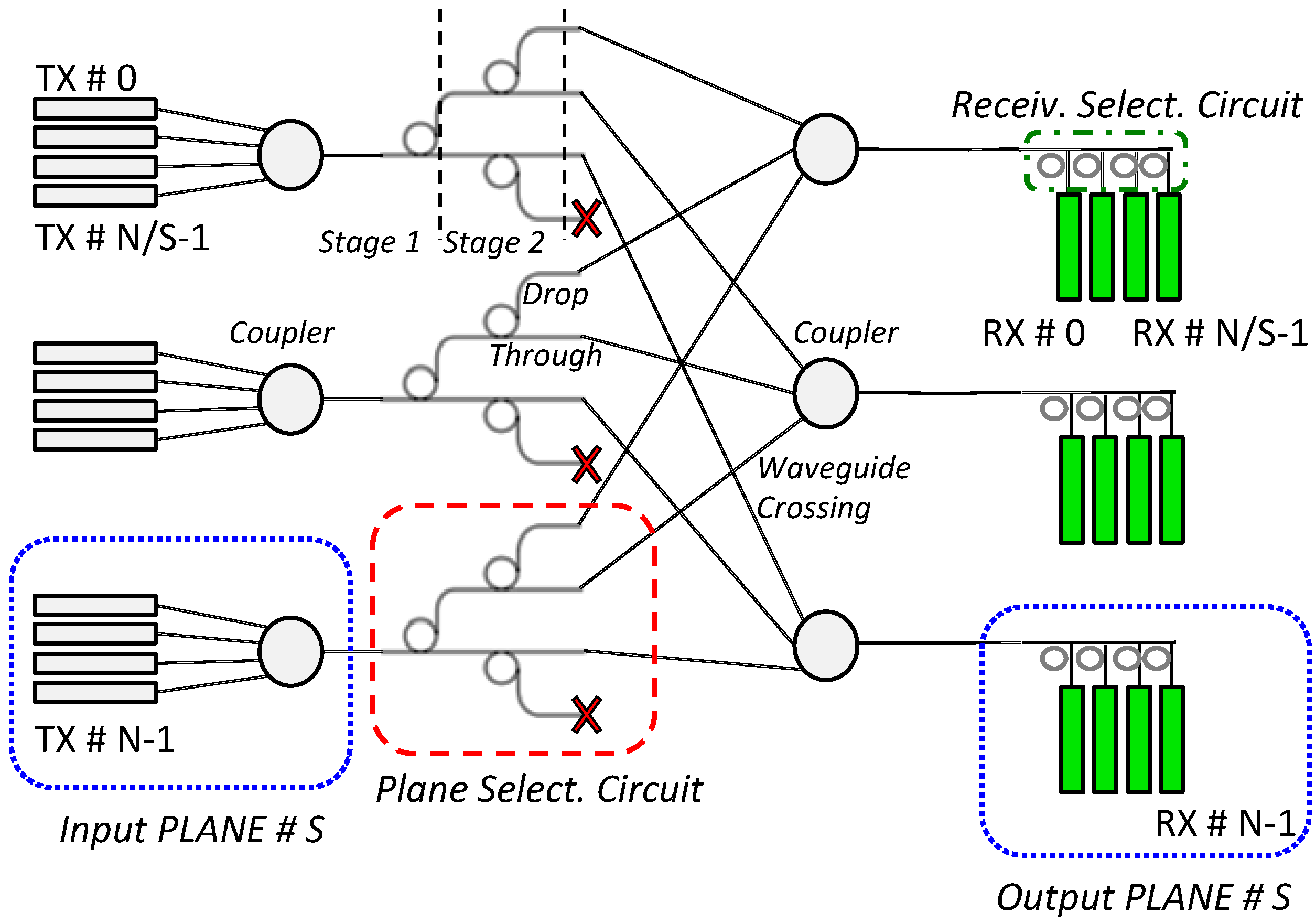
2. Optical Interconnection Architecture

In this section we briefly introduce a general multi-plane switching architecture, which is the basis, technology-independent version of the RR-based switching backplane we have investigated in this study, followed by a description of the design procedure for routing assignment.
The RR-based switching backplane exploits transmitter wavelength tunability as switching mechanism: wavelength h selection by the source LC transmitter is then translated into selection of a target destination LC by means of a passive wavelength-routing structure composed of waveguides, star couplers, and RRs.
In Figure 1, N line cards, each one comprising a tunable-wavelength transmitter (TX) and a fixed-wavelength receiver (RX), are divided into S Input-Output planes (h from 0 to S-1); at each Input plane, N/S TXs are connected to the plane selection circuit (PSC). For instance, TX and RX of each LC are depicted as separated, though they are actually co-located on board of each LC. Routing properties of such a circuit let each TX select the output port corresponding to the plane a certain RX belongs to. Each selection-circuit output port is connected to one of the S couplers (SCs) ( S:1 ) that convey signals in order to set-up connections between TXs and RXs which lie into different planes. Signals coming from different transmission planes are coupled together and an Erbium Doped Fibre Amplifier (EDFA) is placed to restore signal optical power. A receiver selection circuit (RSC) separates channels directed to different RXs of the same Output plane. The number of planes S is allowed to range from 1 to N. If N/S Photonics 01 00131 i003ℕ, then [N/(S-1)] cards will be connected to the first S-1 planes, while the remaining ones will occupy the first available positions within the last plane.
Figure 1. General multiplane switching architecture.
Photonics 01 00131 g001

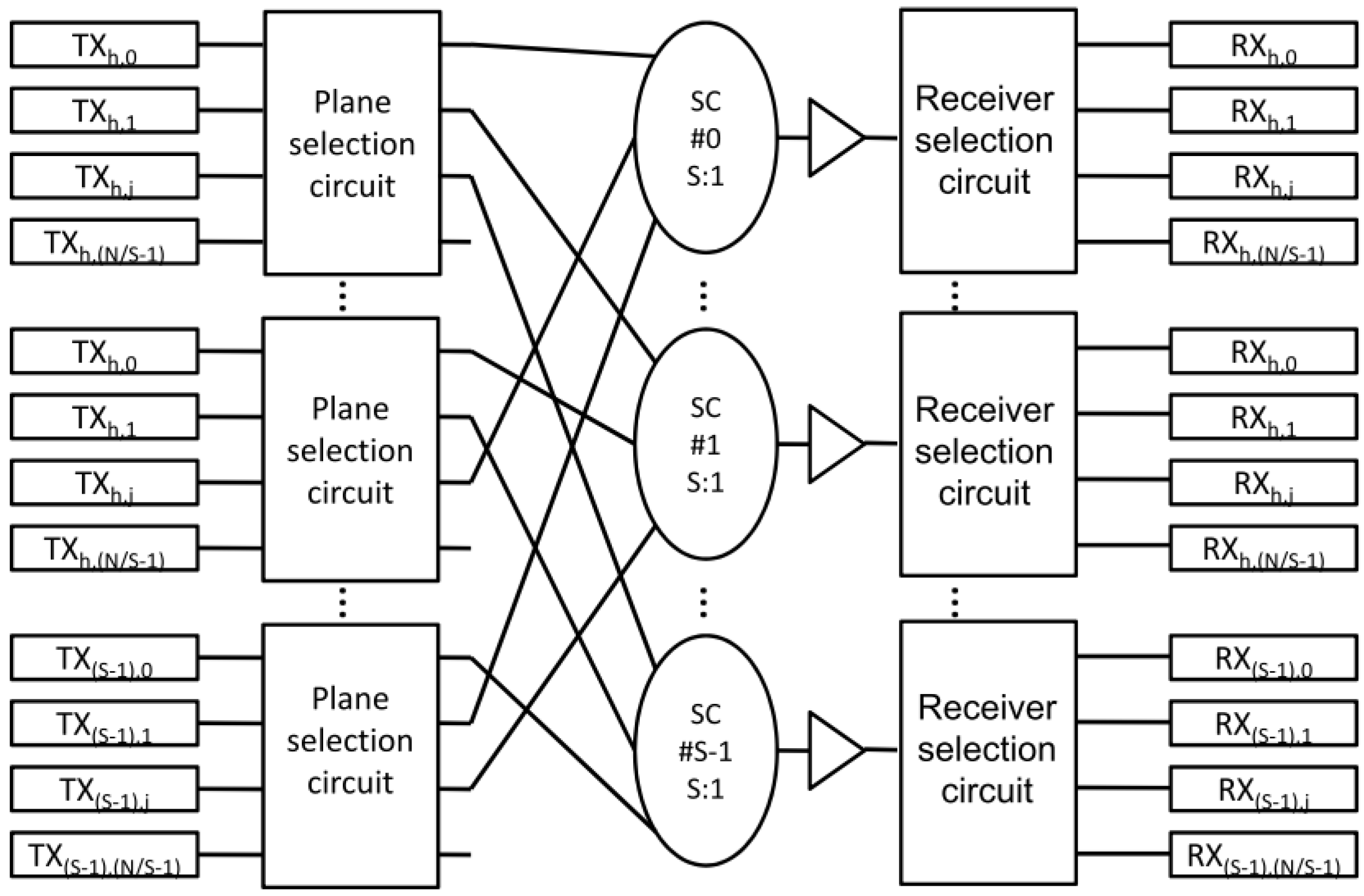
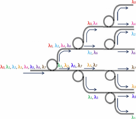
2.1. Ring Resonator Based Backplane

The switching backplane we aim at investigating in this work is shown in Figure 2. A Binary-Tree Ring Router (BTRR), used to select the output plane, acts as PSC whereas an RR array demultiplexer represents the RSC. We assume that only point-to-point connections are established between TXs and RXs, with no output contention, i.e., each RX is to be connected to at most one TX using one single wavelength.
Figure 2. Ring Resonator-based switching architecture.
Photonics 01 00131 g002
The principle of the PSC tree-structure is the same as that based on a cascade of Mach-Zehnder filters, the so-called interleaving. An interleaver is a multi-stage demultiplexer with T stages where at each stage an RR spatially discriminates the incoming wavelength-channels partitioning them into two alternate sub-groups, sending half of them towards the “through” port and half of them towards the “drop” port. Note that, compared to Figure 1, this is a completely passive switching architecture as we do not investigate the use of EDFA before the RSCs. The number of stages T has to be large enough to completely discriminate all the S switching planes, thus T = (log2(S)). The j-th stage will be composed of 2(j − 1) RRs, with 1 ≤ j≤ T and after j stages 2j planes can be selected.
Ring resonators are infinite-impulse response filters with a periodic transfer function of the input frequency [4]. The family of resonance wavelengths λres at which the transfer function has its peaks is βneffLr = 2πN, where β = 2π/λres, neff is the effective refractive index, Lr is the geometrical ring length and N is an integer number (N ≥ 1). The period of the transfer function is knows as Free Spectral Range (FSR) and is given by FSR = c/(2πngR), where c is the speed of the light, ng is the group index and R is the ring radius. The FSR is inversely proportional to the ring radius R. The smallest achievable radius is constrained by the fabrication technology and optical losses inside the ring increase as well with bending [8].
Let us consider a tree-structure composed of three stages as in Figure 3a. If we assume that λ(i,j) is the resonance wavelength of the i-th ring of the j-th stage, the first ring of the first stage has to be dimensioned with a FSR = 2Δλ and λres11 = λ0, then both rings of the second stage have FSR = 4Δλ but λres12 = λ0, λres22 = λ1. Each ring of the third stage is dimensioned with FSR = 8Δλ where λres14 = λ0, λres24 = λ2, λres34 = λ3, λres44 = λ1 are the resonance wavelengths of ring resonators respectively. As an example, Figure 3b shows general ring drop port transfer function of the first, second, and third stage respectively. The −3 dB bandwidth of drop port transfer function can be very narrow, thus, showing higher filter selectivity than the through port [4].
Figure 3. (a) Three stages BTTR; (b) Drop port transfer function of a three stages BTTR.
Photonics 01 00131 g003
The RR array demultiplexer RSC has to separate at most N/S optical channels (see Figure 2) spaced as 2TΔλ; therefore each RR of the considered array is designed with a FSRRSC = N/S 2TΔλ centered at a fixed wavelength. In order to set up a connection between a TX and a given RX on a certain Output plane to which the λx is assigned, the TX has to be tuned on the λx.

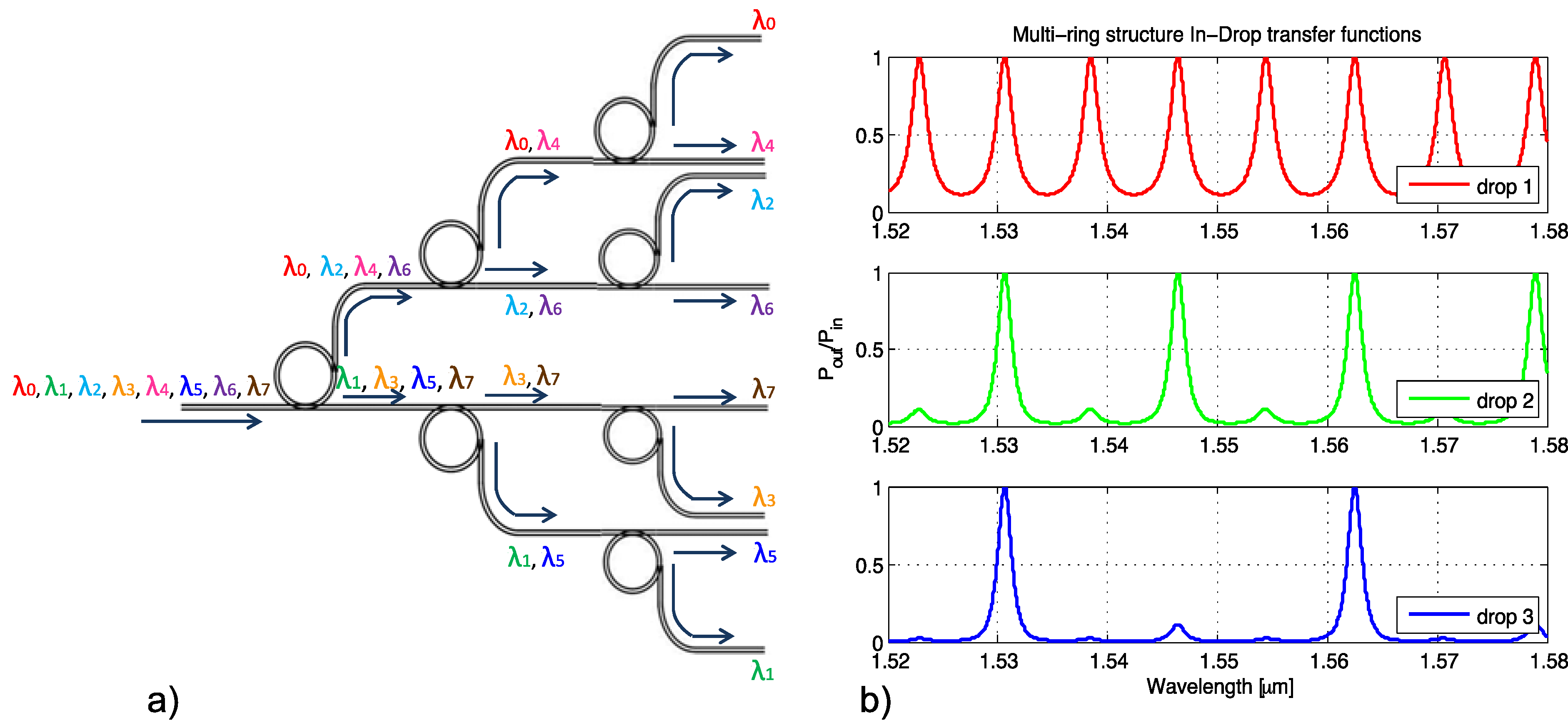
2.2. Backplane Transfer Function

Once each RR is designed (i.e., setting its physical parameters on the basis of the target filter-function physic [8]), we have used the Advanced Simulator for Photonic Integrated Circuits (ASPIC) [9,10] to calculate the transfer function of the backplane. Figure 4 shows the transfer function of a certain TX-RX pair from the architecture shown in Figure 2 with S = 4 planes and N/S = 8 TX/RX per plane. The grey vertical bars represent optical channels at 10 Gb/s with 0.4 nm (50 GHz) spacing. Typical parameters used to assess the performance are: in-band insertion losses (IL), bandwidth at −3 dB from the resonance peak (B3 dB), adjacent channel cross-talk (XT) (XA) and non-adjacent channel XT (XNA). When considering the transfer function of all TX-RX pairs, other parameters are defined: <IL> is the average insertion-loss value across filter resonance peaks; ILm and ILM are the best and worst insertion loss, respectively; Bm and BM are the smallest and largest −3 dB bandwidth, respectively; and XFL represents the worst-case floor XT (i.e., the gap between ILM and the ground XT).
Besides the amplitude response of the architecture, in this study we also take into account the phase response Φ(ω). Actually, the most important parameter which is used to be investigated is the group delay, which is defined as: τg = −(ω)/ = λ2dΦ/(2πcd·λ). The group delay represents the time that a signal takes to pass through a filter. Usually, frequency components of the signal spectrum emerge from the filter with a changed time relationship as they propagate with different velocities and it can cause signal distortion and pulse broadening [11]. It is also worth mentioning that the derivative of the group delay with ω is the second order dispersion which is expressed in (ps2) and it can be calculated as D = g/ or, equivalently, by D = λ2d·dτg/(cdλ) expressed in (ps2/nm).
Figure 4. Backplane transfer function of a certain TX-RX pair.
Photonics 01 00131 g004
Figure 5a shows a typical “drop” port transfer function of a ring resonator and its group delay. Optical −3 dB bandwidth is set to 20 GHz. Figure 5b shows the “through” port transfer function and its group delay. It is evident that for the latter the dispersion is negligible as the group delay is constant and all the frequency components near to the resonant frequency roughly experience the same “pass-through” time. On the other hand, drop port exhibits a group delay distortion due to a non-linear phase response of the filter. At the resonance, the group delay increase with the finesse, which is the ratio between the FSR and the bandwidth, whereas, for the through, port it becomes no longer significant. Second order dispersion is zero at the resonance peak, leading to a small contribution of the third order dispersion on the pulse shape. In our architectures, on the basis of the number of stages of the PSC, signals pass through a given number of ring resonators. Thus, transfer functions show different values of the performance parameters since they are related to the particular path through the architecture a certain signal is routed.
Figure 5. Transfer function “-” and group delay “- -” at the (a) drop port and (b) through port of an RR.
Photonics 01 00131 g005
In Figure 6 we report the transfer functions just before the RSC of the architecture in Figure 2 with S = 4 planes and N/S = 4 TX/RX per plane. The first picture (architecture receiver plane 1) is given by two drop port pass-through. In fact, it has the highest peak of the group delay and the smallest bandwidth. It is worth noting that compared to Figure 5a, the group delay is almost doubled while retaining its shape and the insertion loss is increased of about 1 dB. The same considerations apply for the reception plane 3, as signals traverse two through ports. The reception plane 2 is reached after traversing a combination of one drop and one through port. In fact, it is half way from a totally flat response (reception plane 3) and a Gaussian shaped transmission and group delay (reception plane 1). Finally, the response at plane 4 has a shape, which is driven by the last drop port signals have to pass through. Note that signals are received after traversing another drop port at the specific RSC, thus, the final transmission and group delay are once more “drop port-shaped” before the RX. This is shown in Figure 7 for all the RXs at plane in the architecture reported in Figure with S = 4 planes and N/S = 4 TX/RX per plane.
Figure 6. Transfer function “-” and group delay “- -” after the PSC at different planes.
Photonics 01 00131 g006
Figure 7. Transfer function “-” and group “- -” delay at RXs after the RSC at plane 1.
Photonics 01 00131 g007
The group delay gives a hint of the pulse spread at the RX. In fact, it is the reciprocal of the group velocity (i.e., the propagation velocity of a group of waves whose frequencies are distributed over an infinitesimally small bandwidth centered on frequency f0) multiplied by the propagation distance. If we suppose f1 and f2 being the leading edge and the tail frequency of a spectrum centered around f0, the pulse spread can be determined by taking the difference between the group delay at frequency f0 and that at either f1 or f2 [11].

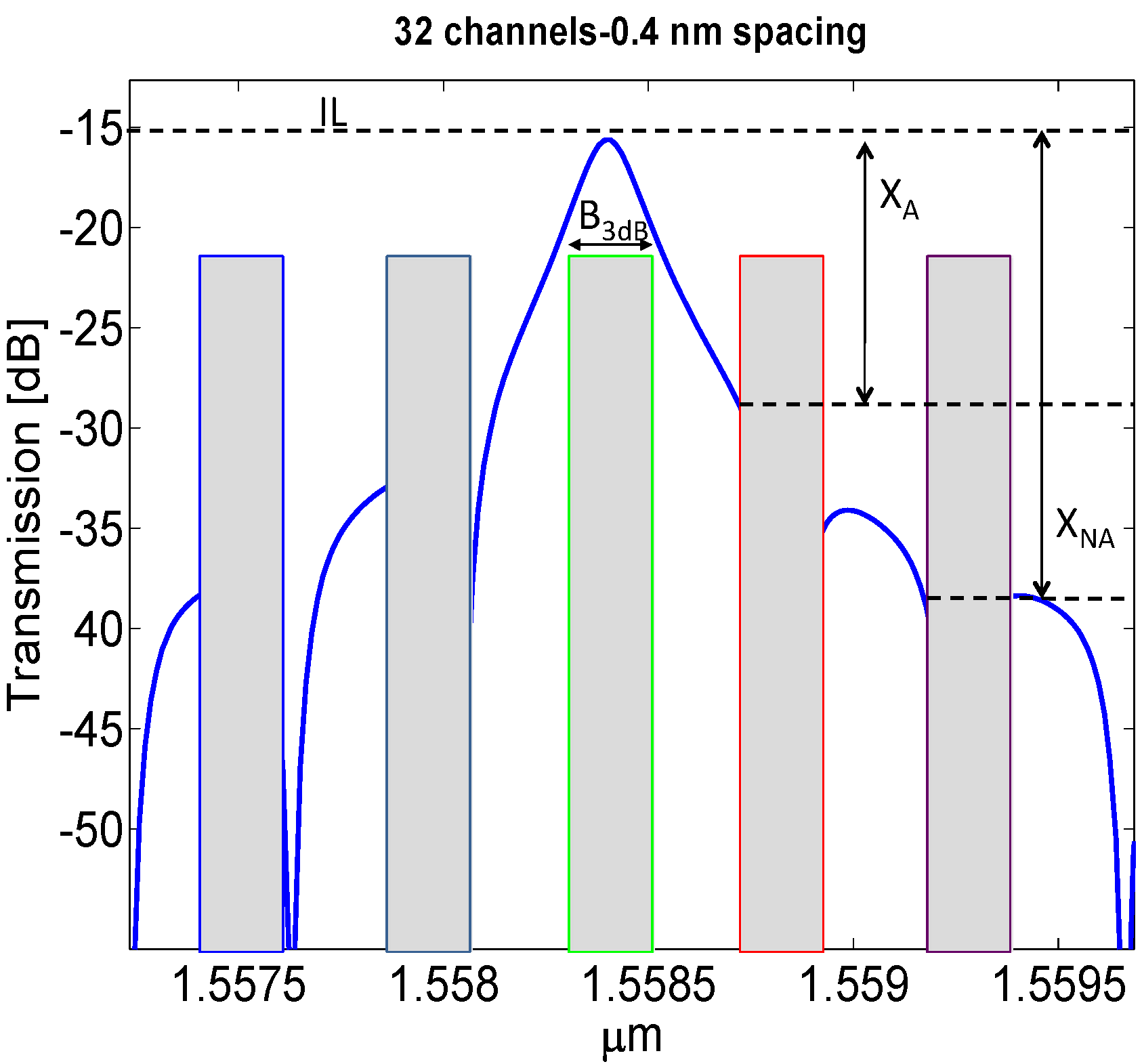
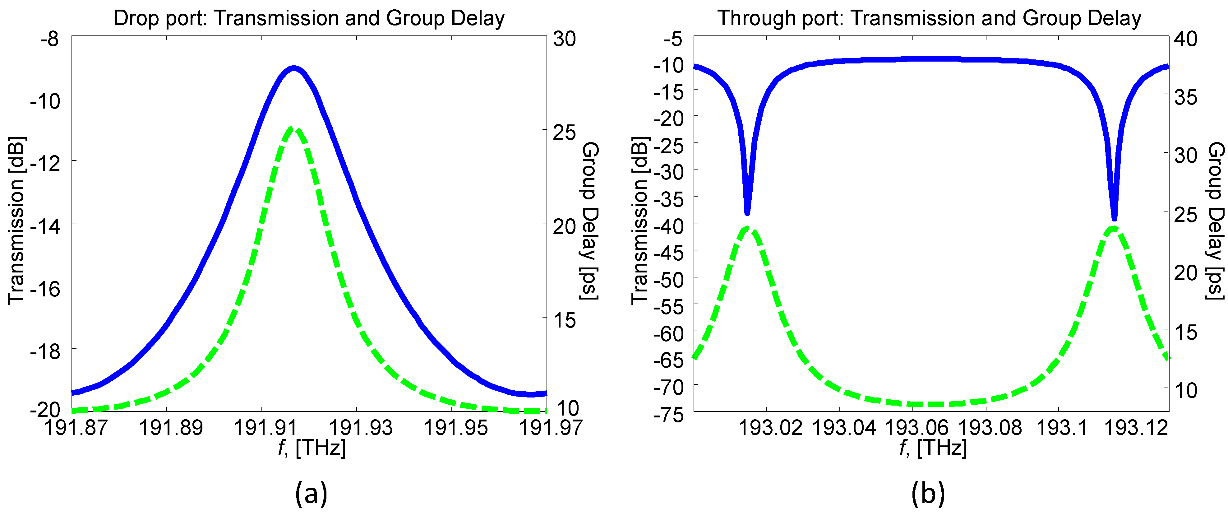
3. Illustrative Numerical Results

In this section, we report numerical results of our performance assessement procedure applied to the proposed architecture. We have investigated the feasibility of our backplane design considering typical implementation issues: number of line cards, switching element-round trip losses, frequency drifting due to thermal variations and waveguide-crossing effects.

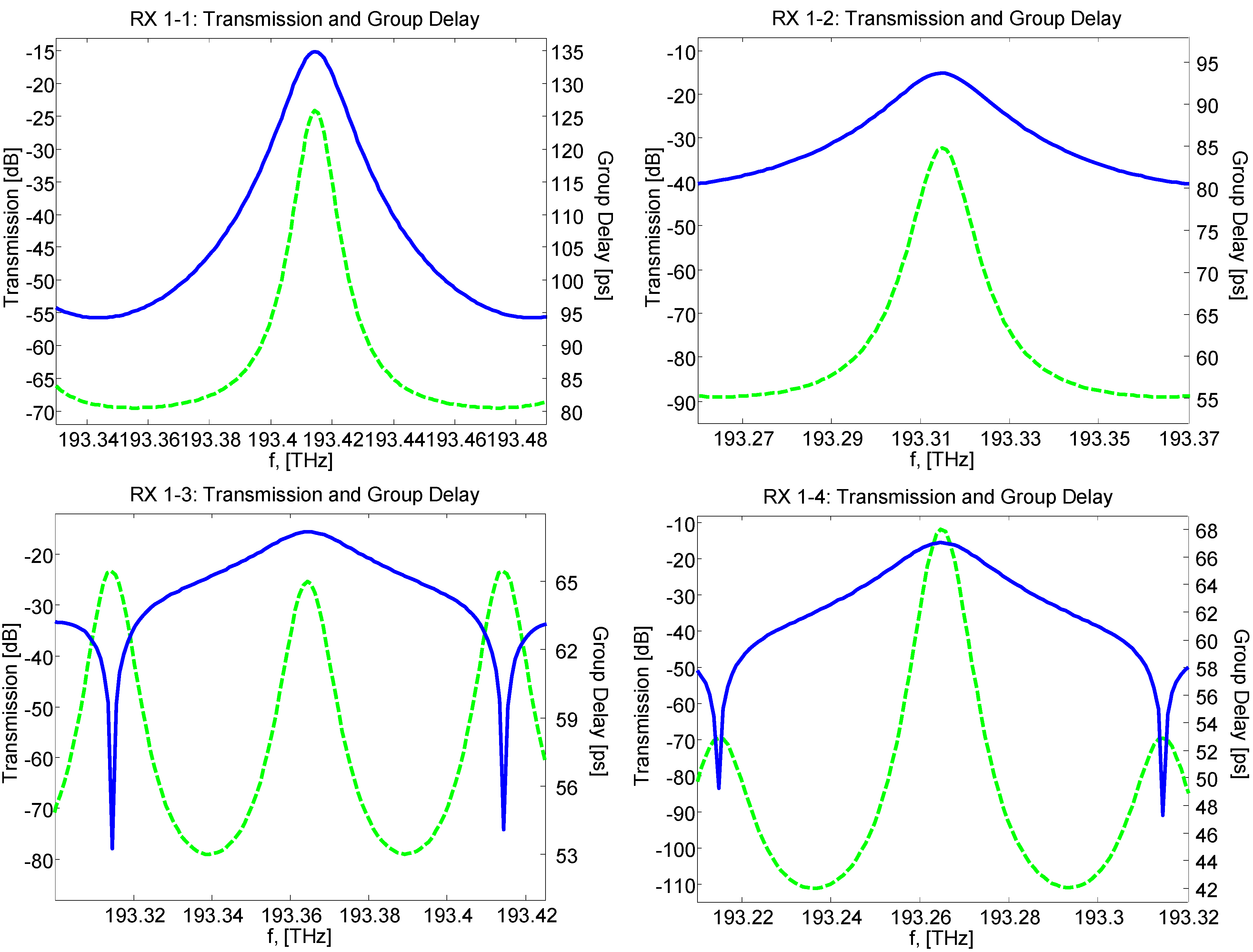
3.1. Number of Optical Channels (λ)

We have evaluated the performance parameters for the following optical-channel configurations: 16 × 10 Gb/s (100 GHz spacing), 32 × 10 Gb/s (50 GHz spacing), and 64 × 10 Gb/s (25 GHz spacing), i.e., N = 16, 32, 64, S = 4 and N/S = 4, 8, 16). We have designed each RR with a −3 dB bandwidth set to 20 GHz.
Insertion loss increases when the number of channels scales up, due to star coupler/splitter losses that increase with N/S (see Table 1). The variability among TX-RX transfer-function peaks is due to the increasing number of cascaded RRs in the RSC (i.e., N/S = 4, 8, 16). The Bm usually corresponds to a RX on the first output plane as signals traverse two drop functions in the PSC, whereas BM corresponds to a RX on the third plane as signals traverse two through functions. The analysis shows that performance parameters are critically low at 25 GHz spacing, while they are fair at 50 GHz and even better at 100 GHz. In the following we show results for 32 channels, since a typical core router hosts 32 LCs at 10 Gb/s [12].
Table 1. Increasing channels at fixed spectrum.
λ<IL>ILmILMBmBMXAXNAXFL
Chan@GHz[dB][dB][dB][GHz][GHz][dB][dB][dB]
16@100−12.5−12−1410.220.9−21.2−27.2−32
32@50−15.8−15−17.610.420.1−14−20.8−29
64@25−19.8−18−22.510.517.6−7.2−15.2−18

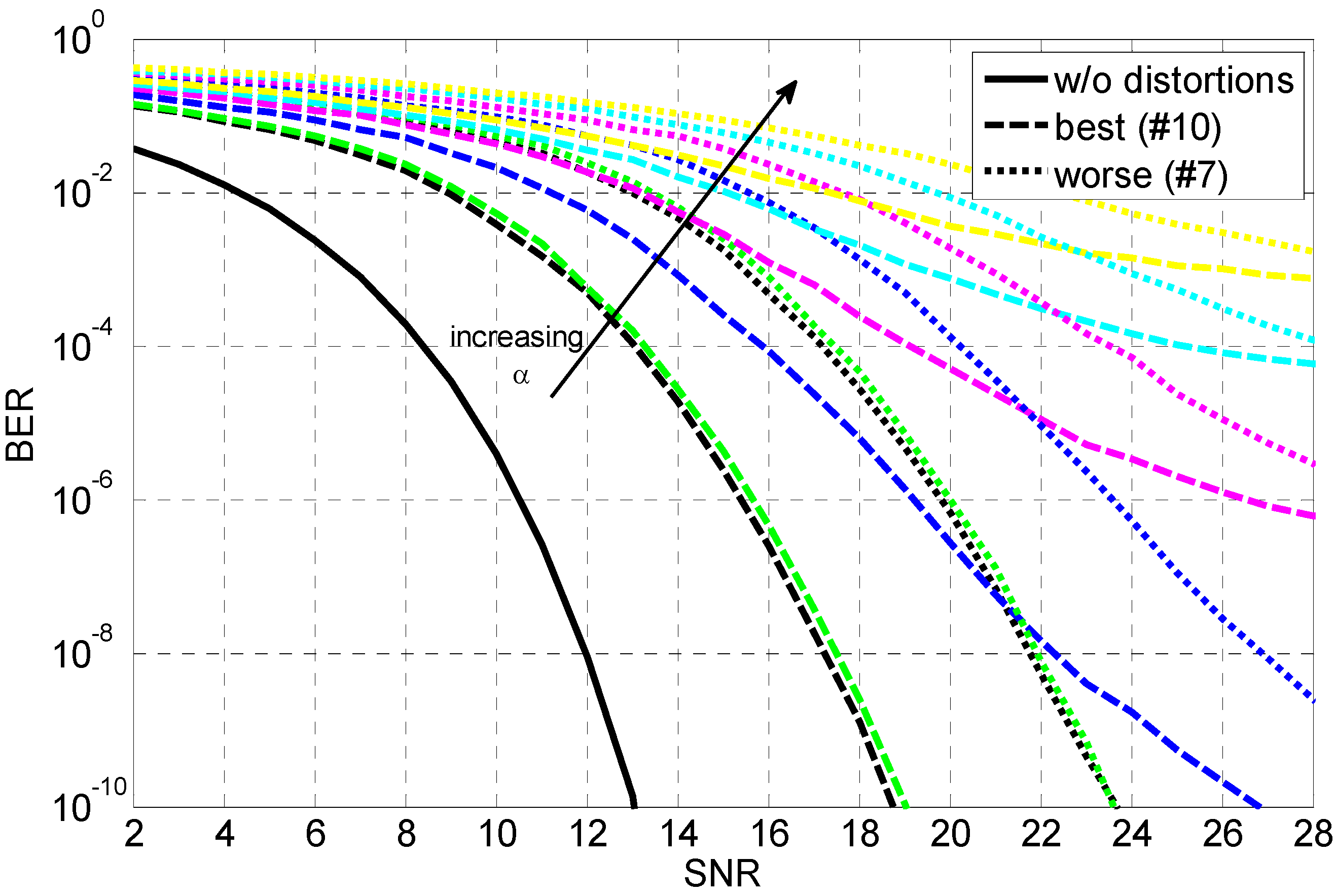
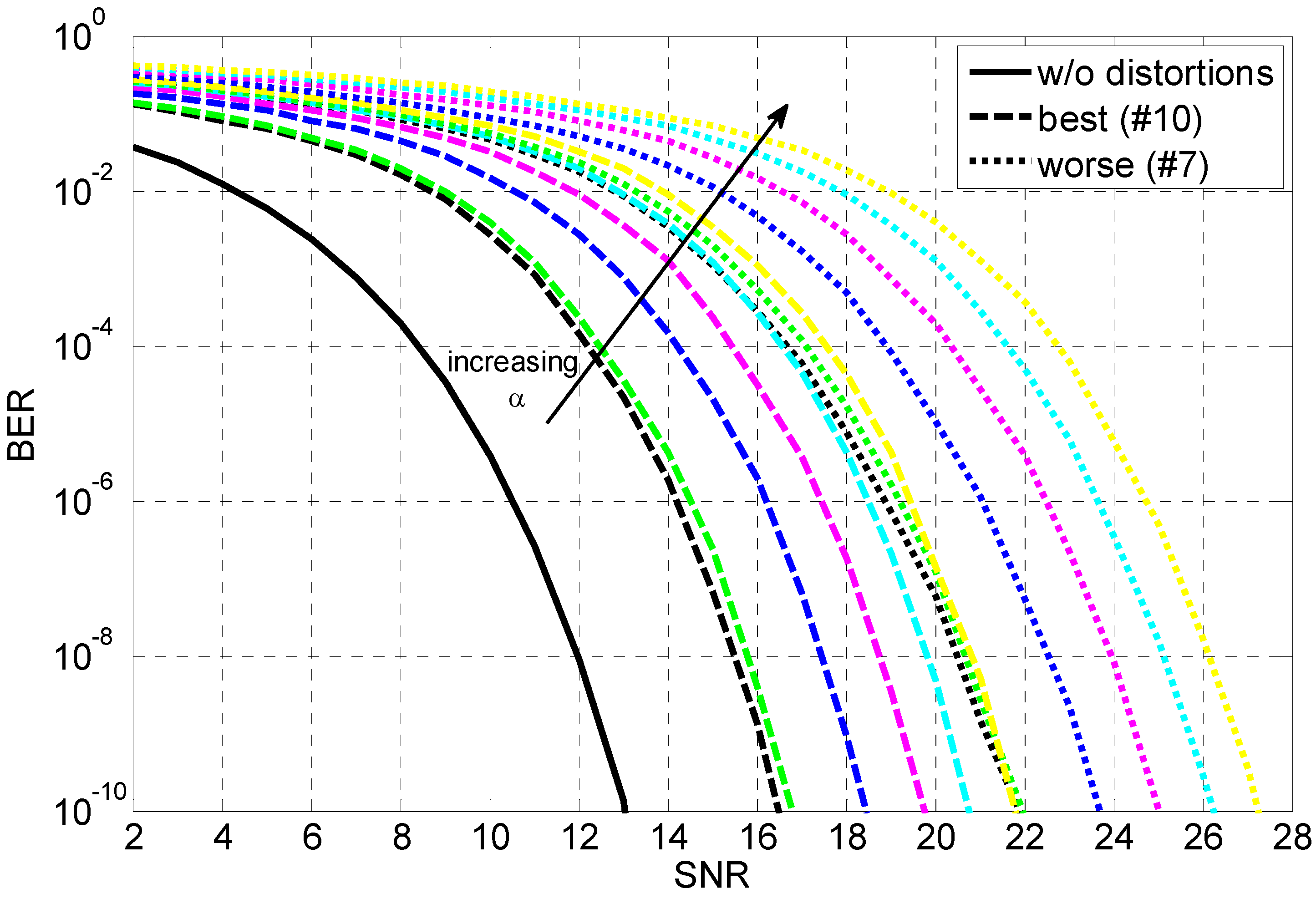
3.2. Roundtrip Loss of Ring Resonators (α)

The effect of roundtrip loss on the RR transfer function is to increase the drop insertion loss and, when various rings are cascaded, also to widen the bandwidth (i.e., the filter becomes less selective). Table 2 reports the values of the investigated parameters. The impact of the paths through the PSC is dramatic. BM and Bm remarkably increase, causing an increase of XT. It is worth noting that loss also makes the variability of IL across different channels to increase due to the low selectivity of filters and high IL at the drop port.
Table 2. Increasing loss/turn, 32@50 GHz.
α<IL>ILmILMBmBMXAXNAXFL
[dB/turn][dB][dB][dB][GHz][GHz][dB][dB][dB]
0−15.8−15−17.610.420.1−14−20.8−29
0.2−20.2−19.5−21.512.231.4−9.7−17.3−24
0.4−23−22.6−24.513.541.2−9.4−14.8−22
0.6−25.9−24.7−27.114.951.1−7.9−13−20
0.8−28−26.4−29.414.957−6.7−12.2−17
1.0−29.6−27.8−31.415.962−5.9−11.2−14

3.3. Thermal Variations (ΔT)

The change in the refractive index of a material as a function of the variation of temperature is known as the thermo-optic effect. An unintentional waveguide temperature variation turns into a resonance-frequency drifting: e.g., ΔT = 1 °C, corresponds to 10 GHz frequency shift (in silicon) [13]. We have investigated the impact of such thermal perturbation on the overall backplane transfer function when a value within the range ±0.5, ±1, and ±1.5 °C of thermal variation is applied to any RR with uniform probability distribution. Table 3 shows that a thermal drifting of ±1.5 °C has a detrimental impact. In fact, the transfer functions are highly distorted and the variability on IL (measured as gap between ILm and ILM) increases from almost 2 to 6 dB. Our architecture is clearly sensitive to thermal variations higher than 1.5 °C.
Table 3. Resonance frequency drifting, 32@50 GHz.
ΔT<IL>ILmILMBmBMXAXNAXFL
[°C][dB][dB][dB][GHz][GHz][dB][dB][dB]
0−15.8−15−17.610.420.1−14−20.8−29
±0.5−15.9−15.3−17.811.919.8−12.7−19.7−29
±1.0−16.2−16−18.411.620.1−12.2−20.4−27
±1.5−16.5−15.3−21.610.720.3−11.6−15.7−23

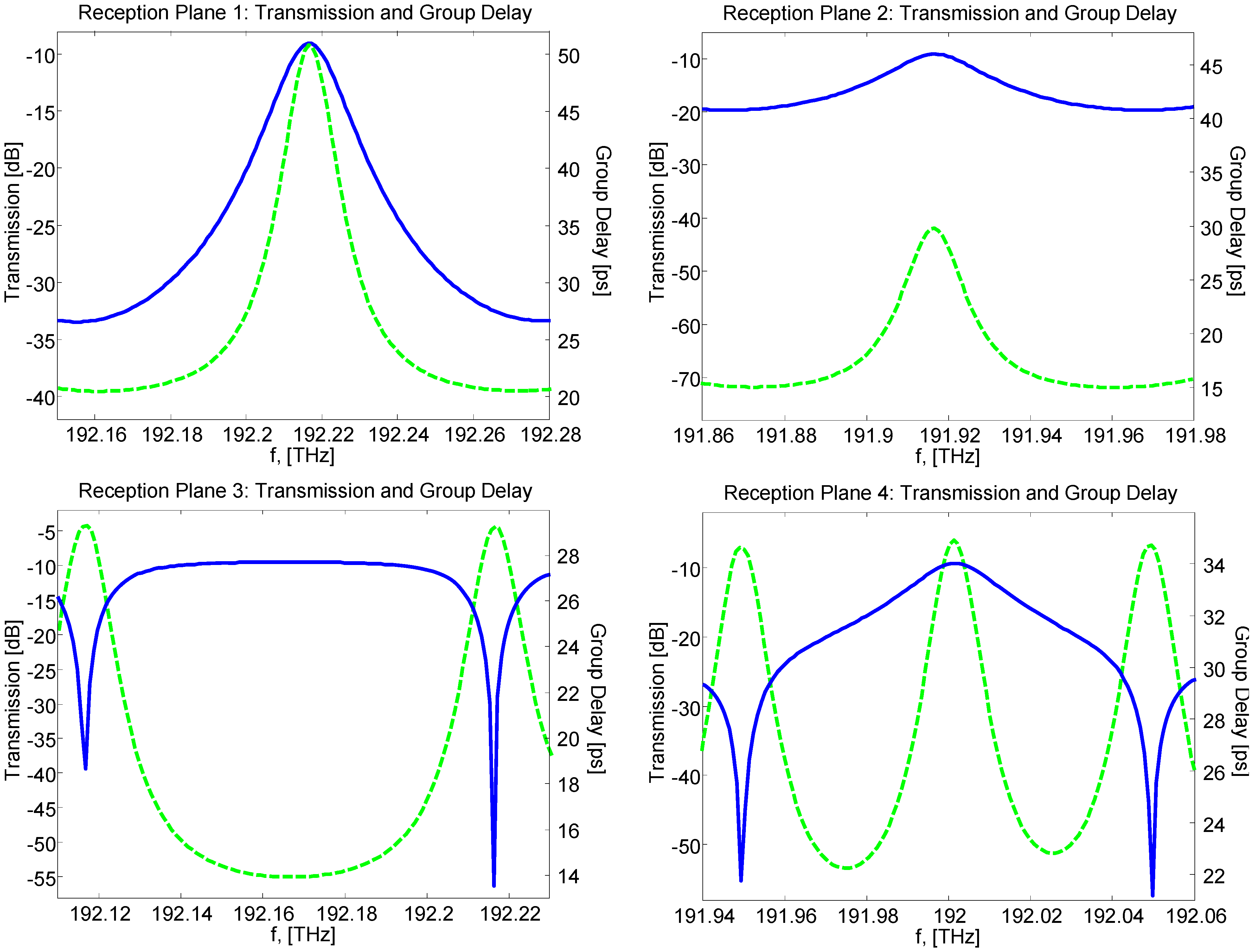
3.4. Waveguide Crossing

There are three major impairment contributions related to waveguide crossing: Crossing Insertion Loss (CIL), Crossing Reflected Power (CRP) and Crossing XT (CXT) power, the latter due to adjacent waveguide power coupling [14]. Such impairments depend on the crossing angle. We consider values that are related to the orthogonal waveguide crossing, which represents the best-case, since such a condition can be achieved by a careful geometric design of the waveguides.
CIL increases the variability of IL among channel resonance peaks since signals directed to different Output planes may traverse a different number of waveguide crossings. The gap between ILm and ILM increases from almost 3 to 4 dB when setting CIL up to 1 dB; nevertheless, XT level values scale down along with peak loss.
CRP above 2% is highly detrimental. It causes high variability of channel IL, resonance frequency shifting and severe distorsion. Moreover, high values of XT have been found, the worst case is XA = −10 dB and XNA = −15 dB. The most detrimental impairment is the waveguide CXT power. In addition, in this case, values higher than 2% may impair feasibility. <IL> varies from −15 dB of the 0% case to −21 dB of the 15% and the worst-case gap between ILm and ILM is 11 dB.

3.5. Technology Remarks

In the proposed architecture, the FSR of RRs in RSC drives the choice of the technology to be used (see Design Section). As for the PSC of our reference architecture (32 chann./50 GHz, 2 stages), the FSR of last-stage RR is 200 GHz while for the RSC, the FSR of each RR is 1.6 THz, corresponding to rings with radius = 7 µm, thus, the choice of silicon becomes mandatory [7]. Smaller rings, that is, wider FSR, are difficult to achieve in practice.

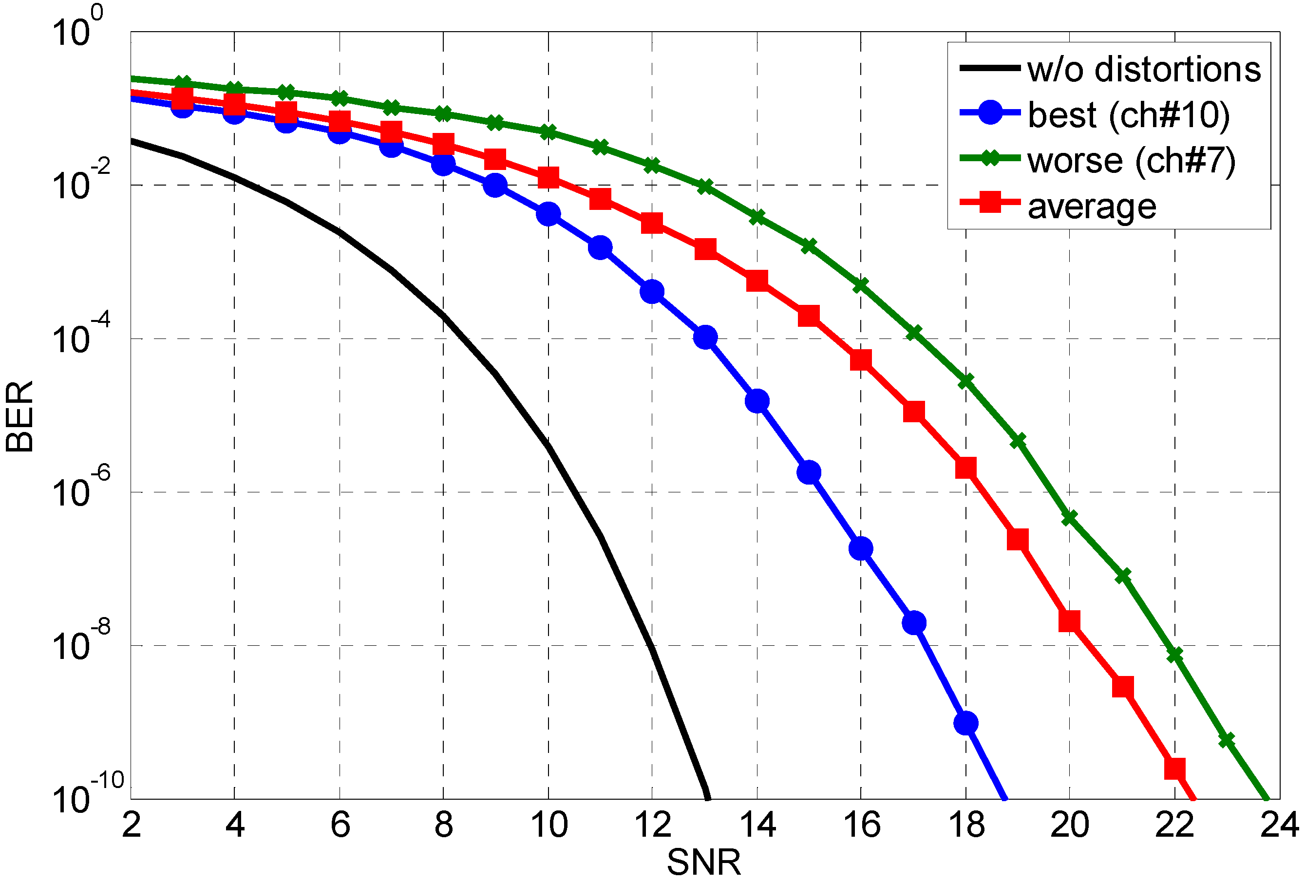
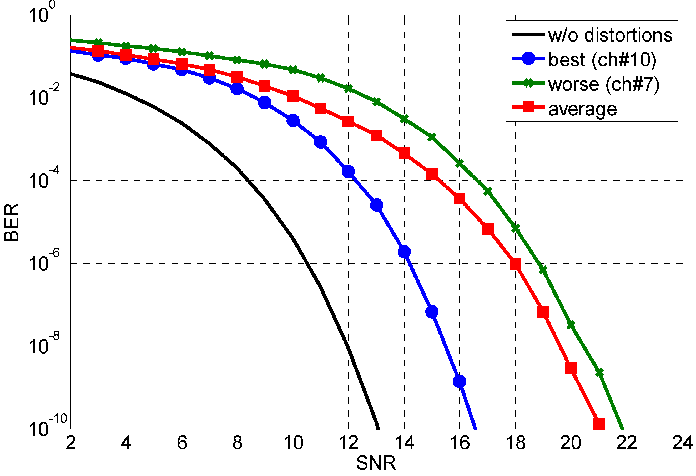
4. BER Performance Analysis

Direct detection for transmission at 10 Gb/s of 32 OOK-NRZ signals spaced at 50 GHz is considered. For BER performance analysis the impulse response used for pulse shaping was chosen with a rise and fall time of 35% the bit duration. As is known, the effect of filtering operations performed by a certain TX-RX pair on the input signal and the resulting distortions can be estimated by means of the eye diagram [15]. In order to evaluate the distortions introduced by optical filtering, we consider the case where the detected signal is dominated by the photo-detector thermal noise. Under this assumption the Q factor can be calculated from the eye diagram as:
Photonics 01 00131 i001
where µ1 and µ0 are the average voltages associated to the levels 1 and 0 at the eye center, respectively, while σ1 and σ0 are the effective standard deviations associated to the levels 1 and 0, respectively. The Q factor allows for estimating the BER associated to the received signal after its conversion into the electrical domain by using the formula:
Photonics 01 00131 i002
Each signal transmitted at a specific wavelength has been filtered by the PSC transfer function and then selected by the corresponding RSC transfer function. The eye diagram has been evaluated for each of the transfer functions resulting from all the TX-RX pair combinations. Figure 8 shows the best, the worse and the average BER performance versus the electrical Signal-to-Noise Ratio (SNR) obtained considering the case of roundtrip loss α = 0. The electrical SNR is given by the ratio of the signal power and noise power after electrical filtering with the same bandwidth as that of the RSC. As a reference, in the Figure, the BER performance obtained in the ideal case, i.e., without signal distortions, is also reported. From the curves we observe that the SNR loss of the average case with respect to that without (w/o) distortions varies between 6 dB, at BER = 10−2, and 8 dB, at BER = 10−10. In the same range of BERs, the SNR loss of the best channel with respect to that w/o distortions is comprised between 3.5 and 4 dB. The SNR gap between the best and the worse performance associated to channel #10 and channel #7, respectively, varies between 4 dB, at BER = 10−2, and 5 dB, at BER = 10−10.
Figure 8. BER vs. SNR for transmission at 10 Gb/s of NRZ-OOK channels with roundtrip loss α = 0. The best performance was obtained for channel #10, the worse for channel #7 and the average considering the mean over the 32 channels.
Photonics 01 00131 g008
Figure 9 reports the best and the worst performance associated to channel #10 and channel #7, respectivily, for increasing values of the roundtrip loss α = 0, 0.2, 0.4, 0.6, 0.8, 1. From the figure we observe that for a given value of α the SNR gap between the best and the worse channel is approximately always the same. Moreover, an SNR loss of approximately 5 dB can be observed between α = 0 and a = 1.
Figure 9. BER vs. SNR for transmission at 10 Gb/s of 32 NRZ-OOK channels with increasing roundtrip losses α = 0, 0.2, 0.4, 0.6, 0.8, 1. Dashes curves: best channel (#10); dotted curves: worse channel (#7).
Photonics 01 00131 g009
The effect of XT on the BER is shown in Figure 10. We have verified that in order to evaluate the effect of XT on the channel of interest it is enough to consider only the effect of the two more adjacent signals. From Figure 10 we observe that the SNR loss of the average case compared to that w/o distortions increases of only 0.2 dB at BER = 10−2 with respect to the situation without XT considered in Figure 8 while it increases up to 1.3 dB at BER = 10−10. The loss in SNR of the best case with respect to the ideal case w/o distortions is comprised now between 4.5 dB at 10−2 and 6 dB at 10−10. It is worth noting that the SNR gap between the best and the worst case remains the same as that without XT.
In Figure 11 the effect of XT on the best and the worse performance is reported for increasing values of the roundtrip losses α = 0, 0.2, 0.4, 0.6, 0.8, 1. In contrast to the analogous situation without XT considered in Figure 9, in this case we observe that for the values of α equal to 0.6, 0.8 and 1 the BER presents an error floor. This effect arises because the presence of some configurations of interference that cause the closure of the eye even in the situation where noise is absent. By comparing the curves reported in Figure 9 and Figure 11 at a given BER it is possible to evaluate the degradation introduced by XT for a fixed value of α.
Figure 10. BER vs. SNR for transmission at 10 Gb/s of 32 NRZ-OOK channels with roundtrip loss α = 0 in presence of XT.
Photonics 01 00131 g010
Figure 11. BER vs. SNR for transmission at 10 Gb/s of 32 NRZ-OOK channels with increasing roundtrip losses α = 0, 0.2, 0.4, 0.6, 0.8, 1 in presence of XT. Dashes curves: best channel (#10); dotted curves: worse channel (#7).
Photonics 01 00131 g011
It is worth observing that for input signals with rates higher that 10 Gb/s, i.e., 40, 100, and 160 Gb/s an increase of modulation order is required in order to satisfy the bandwidth limitation imposed by the optical filtering. As is well known, high order modulation formats require coherent demodulation and are more sensitive to signal distortions introduced by optical filters and XT. Therefore, in order to achieve a performance that is comparable with that of 10 Gb/s transmission an appropriate signal processing is required.

5. Conclusions

We have presented a new RR-based switching fabric and a novel approach to assess architecture performance. Our transfer function analysis allows us to accurately capture the impact of each design issue with respect to the ideal scenario. This capability is not achievable in power budget and XT power penalty evaluations. In this work, we have analyzed the OI architecture in terms of optical performance parameters and signal distorsions introduced by the filtering operations performed by PSC and corresponding RSC for a given value of the wavelength of the input signal. From the observation of the eye diagrams for all the TX-RX pairs in case of OOK-NRZ transmisison at 10 Gb/s, performance analysis has been worked out by estimating the BER both without and with XT vs. SNR of the proposed architecture.

Acknowledgments

The research leading to these results has received funding from the European Union Seventh Framework Programme (FP7/2007-2013) under grant agreement n. 257740 (Network of Excellence “TREND”). This manuscript is an invited paper as part of the Special Issue on “All Optical Networks for Communications” published in Photonics.

Author Contributions

Giuseppe Rizzelli, Domenico Siracusa and Guido Maier jointly designed the switching architecture. Maurizio Magarini defined the analysis procedure used for BER computation, while Mehmood Alam performed the BER simulations; Giuseppe Rizzelli also carried out the transfer-function evaluation of the architecture, exploiting integrated-optics analysis software and supervision provided by Andrea Melloni.

Conflicts of Interest

The authors declare no conflict of interest.

References

  1. Korotky, S.K. Traffic trends: Drivers and measures of cost-effective and energy-efficient technologies and architectures for backbone optical networks. In Proceedings of the Optical Fiber Communication Conference and Exposition and the National Fiber Optic Engineers Conference, Los Angeles, CA, USA, 4–8 March 2012; p. OM2G.1.
  2. Bianco, A.; Carta, E.; Cuda, D.; Finochietto, J.M.; Neri, F. An optical interconnection architecture for large packet switches. In Proceedings of the International Conference on Transparent Optical Networks, Rome, Italy, 1–5 July 2007; pp. 226–229.
  3. Siracusa, D.; Maier, G.; Linzalata, V.; Pattavina, A. Scalability of optical interconnections based on the arrayed waveguide grating in high capacity routers. In Proceedings of the IEEE International Conference on Optical Network Design and Modeling, Bologna, Italy, 8–10 February 2011; pp. 1–6.
  4. Klein, E.J. Densely Integrated Microring-Resonator Based Components for Fiber-to-the-Home Applications. Ph.D. Thesis, University of Twente, Enschede, The Netherlands, 2007. [Google Scholar]
  5. Melloni, A.; Martinelli, M. The ring-based resonant router. In Proceedings of the ICTON 2003; Warsaw, Poland: 29 June–3 July 2003.
  6. Cuda, D.; Gaudino, R.; Gavilanes, G.A.; Neri, F.; Maier, G.; Raffaelli, C.; Savi, M. Capacity/cost tradeoffs in optical switching fabrics for terabit packet switches. In Proceedings of the IEEE International Conference on Optical Network Design and Modeling, Braunschweig, Germany, 18–20 February 2009; 2009; pp. 1–6. [Google Scholar]
  7. Rizzelli, G.; Siracusa, D.; Maier, G.; Magarini, M.; Melloni, A. Performance of ring-resonator based optical backplane in high capacity routers. In Proceedings of the 15th International Conference on Transparent Optical Networks, Cartagena, Spain, 23–27 June 2013; pp. 1–4.
  8. Melloni, A.; Costa, R.; Cusmai, G.; Morichetti, F. The role of index contrast in dielectric optical waveguides. Int. J. Mater. Prod. Technol. 2009, 34, 421–437. [Google Scholar] [CrossRef]
  9. Filarete srl, Italy. Milano. Available online: http://www.aspicdesign.com (accessed on 11 April 2014).
  10. Melati, D.; Morichetti, F.; Canciamilla, A.; Roncelli, D.; Soares, F.; Bakker, A.; Melloni, A. Validation of the building-block-based approach for the design of photonic integrated circuits. J. Lightwave Technol. 2012, 30, 3610–3616. [Google Scholar] [CrossRef]
  11. “Dispersion”. In Fundamentals of Optical Fibers: Wiley Series in Pure and Applied Optics; Buck, J.A. (Ed.) Wiley-Interscience, John Wiley & Sons: Hoboken, NJ, USA, 2004.
  12. T Series Core Routers. Available online: http://www.juniper.net/ (accessed on 11 April 2014).
  13. Knights, A.P.; Jessop, P.E. Silicon waveguides for integrated optics. In Optical Waveguides: From Theory to Applied Technologies; Calvo, M.L., Lakshminarayanan, V., Eds.; Taylor and Francis: London, UK, 2007; pp. 231–270. [Google Scholar]
  14. Bukkems, H.G. Minimization of the loss of intersecting waveguides in inP-based photonic integrated circuits. Photonics Technol. Lett. 1999, 11, 1420–1422. [Google Scholar] [CrossRef]
  15. Downie, J.D. Relationship of Q penalty to eye-closure penalty for NRZ and RZ signals with signal-dependent noise. J. Lightwave Technol. 2005, 23, 2031–2038. [Google Scholar] [CrossRef]

