1. Introduction
Research activities targeting millimeter wave (mmW) applications,
i.e., applications utilizing electromagnetic waves within the frequency range from 30 GHz to 300 GHz, have been revived in recent years. Many modern applications in sensing [
1], imaging [
2], radar [
3], and, most notably, in wireless communications [
4,
5], make use of ever higher frequencies. One prominent example is that of future 5G mobile systems, which are currently being considered to make use of carrier frequencies in the mmW range [
6,
7]. This has simultaneously revived the interest in solid-state components and it has led to scores of high-performance components enabling, for example, highly-efficient mmW signal generation and detection [
8]. In addition to purely electrical solutions using advanced InP- or SiGe-based solid-state amplifiers and mixers, integrated photonic technology has also become more mature, leading to photonic solutions ready for real-life implementations, e.g., the generation and distribution of low-phase-noise mmW local oscillator signals in radio astronomy [
9]. Additionally, research on broadband wireless communications has led to recent outstanding results using photonic technologies. In particular, radio-over-fiber (RoF) techniques have enabled the transmission of extreme high-data (100 Gbit/s) wireless signals within mmW bands [
10].
High-speed photodiodes (PDs) are key in such broadband RoF wireless networks. To meet the challenging demands for advanced mmW PDs in terms of bandwidth or output power, various groups are researching evolutionary, but also revolutionary, concepts helping to improve the performances of state-of-the-art mmW PDs [
1,
5,
8,
11,
12,
13,
14,
15,
16,
17,
18]. Key objectives of this research are to expand the operational bandwidth of the PDs and simultaneously attain higher power-saturation levels [
1]. High-frequency operation typically leads to PD structure designs including relatively thin absorptive layers to enhance the transit-time-limited response, which on the other hand simultaneously deteriorates the external quantum efficiency, primarily in PDs with top-illumination [
13,
14]. Furthermore, the resistance-capacitance (RC) time constant becomes the dominating limitation in terms of bandwidth for thin, undoped absorbing layers. The necessity to simultaneously achieve high external quantum efficiencies, high operational bandwidths for broadband (or full-band) operation, as well as high radio frequency (RF) output-power levels, favor the use of waveguide-based PDs [
15,
16]. This is due to their flexibility in the layer structure and topology design. As an example, mushroom-type waveguide PDs offer a solution for improving RC limitations, enabling high-frequency operation [
17].
In this work, we report on InP-based 1.55 μm triple transit region PDs (TTR-PDs) [
18], which employ the waveguide approach for hybrid integration with passive optical silica waveguides. As a future application (e.g., for 5G mobile systems), we first propose a scheme of a hybrid-integrated photonic mmW transmitter for photonic RF beam forming and beam steering. Since this approach is based on heterogeneous integration of InP- and silicon-based photonics components, the optical waveguide coupling is to be investigated for connecting the optical beam-steering network (including passive optical silica waveguides) [
19,
20] with a linear TTR-PD array. One of the challenges of these hybrid-integrated waveguide devices remains in the design of an appropriate layer structure, which enables efficient coupling of the optical mode from the passive silica waveguide into the active InP-based waveguide. To study evanescent coupling, we introduce an active waveguide based on the TTR-PD layer structure [
18] on top of a passive optical silica waveguide [
21]. Numerical simulations using the beam propagation method (BPM) are accomplished to demonstrate the optical TE-mode propagation in the hybrid-integrated InP/silica double waveguide. For experimental characterization, several TTR-PD chips were fabricated with monolithically-integrated passive optical waveguides to couple light into the active PD structure and, thus, measure the responsivity (DC and RF), the 3 dB bandwidth, and the 1 dB compression point of the TTR-PDs prior to further hybrid integration with silica waveguides. Accordingly, we report high-power (>0 dBm) TTR-PDs with a measured 3 dB bandwidth beyond 130 GHz.
2. Scheme of a Hybrid-Integrated InP/Silicon-Based Photonic Millimeter Wave Transmitter
For future 5G mobile systems considered to make use of carrier frequencies in the mmW range, e.g., in the 60 GHz or the 70/80 GHz frequency band [
4,
6,
7], photonic mmW transmitters that simultaneously enable high output-power levels, high operational bandwidth, and the opportunity for photonic beam forming, as well as beam steering, are necessitated. For this reason, a hybrid integration of different solid-state technologies on one platform becomes key for such high-performance devices. One of the benefits for a hybrid-integrated waveguide PD would be, for example, the low propagation loss (<0.1 dB/cm) [
21] of the passive optical silica waveguides used in optical beam-steering networks [
19,
20]. A schematic view of a hybrid-integrated InP/silicon-based photonic mmW transmitter is illustrated in
Figure 1.
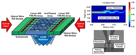
Figure 1.
Schematic view and operation principle of a hybrid-integrated InP/silicon-based photonic millimeter wave (mmW) transmitter featuring two optical silica waveguide (WG) modules, two linear WG TTR-PD arrays and a 4 × 4 phased array antenna for mmW beam forming and beam steering.
Figure 1.
Schematic view and operation principle of a hybrid-integrated InP/silicon-based photonic millimeter wave (mmW) transmitter featuring two optical silica waveguide (WG) modules, two linear WG TTR-PD arrays and a 4 × 4 phased array antenna for mmW beam forming and beam steering.
As depicted in the scheme, the proposed photonic mmW transmitter is composed of different optics (optical waveguide modules), optoelectronics (waveguide TTR-PD arrays), and RF (phased array) sections. Two optical silica waveguide modules are integrated for double-sided illumination at the optical wavelength of 1.55 μm. An optical fiber array with eight conventional (
i.e., cleaved) single-mode fibers (SMFs) is considered for coupling of light into each silica module, which comprises monolithically-integrated spot-size converters [
21] and an optical beam-steering network, e.g., using the true-time-delay approach [
19,
20].
The optical inputs of the linear TTR-PD array are interfaced with the corresponding optical outputs of the passive silica waveguides from the silica module. To couple the light vertically into the active TTR-PD structure, the TTR-PD is to be integrated on top of the passive silica waveguide. In the TTR-PD, the optical signal with the appropriate beam-steering signal (
i.e., phase) gets absorbed and converted into an electrical (mmW) signal that is further fed to an integrated antenna element, which is located on a silicon platform. Each TTR-PD allows individually addressing an antenna element of the phased array. Similar integration approaches on silicon submounts were already reported in previous works on hybrid-integrated InP/silicon-based photonic transmitter modules employing highly-resistive silicon spacers and hemispherical lenses [
22,
23]. Finally, the relative phases of the generated mmW signals can be adjusted in such a way that an efficient mmW beam of the entire phased array is generated and steered in a preferential direction [
19,
20].
4. Experimental Results of Fabricated Waveguide Triple Transit Region Photodiode Chips
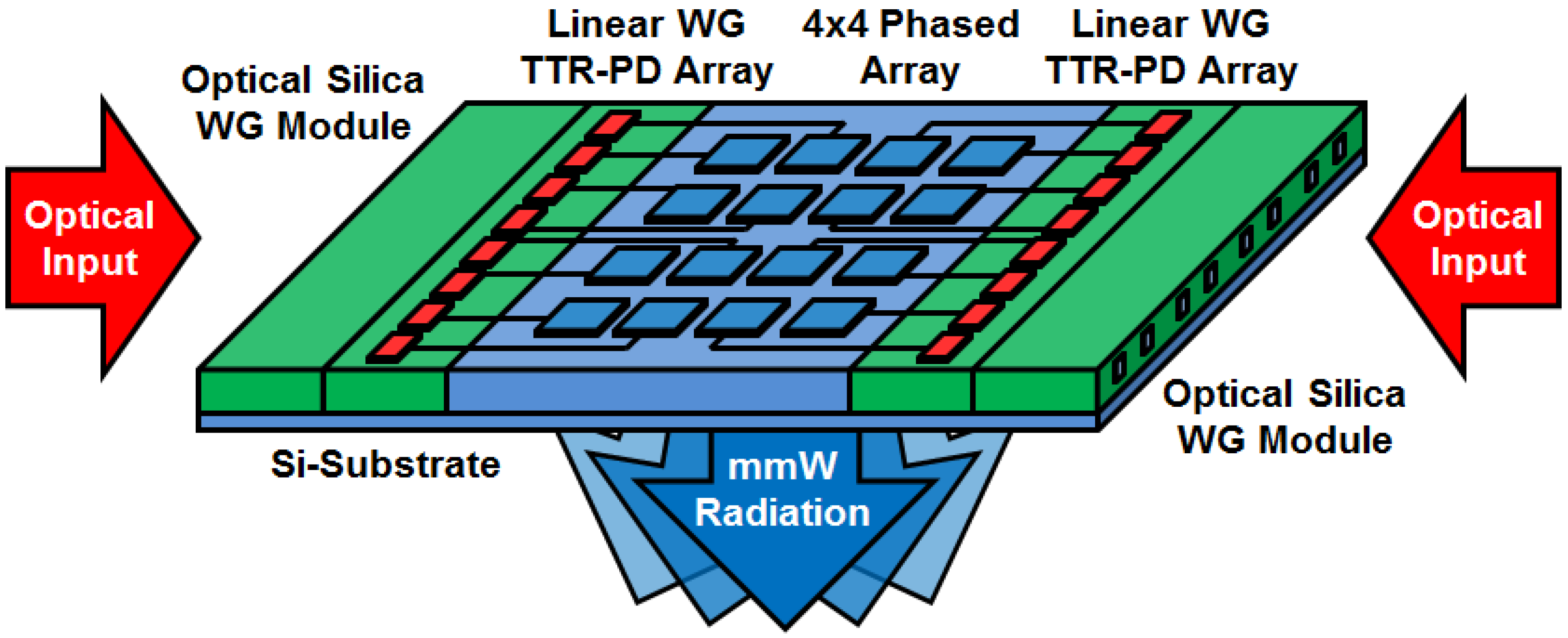
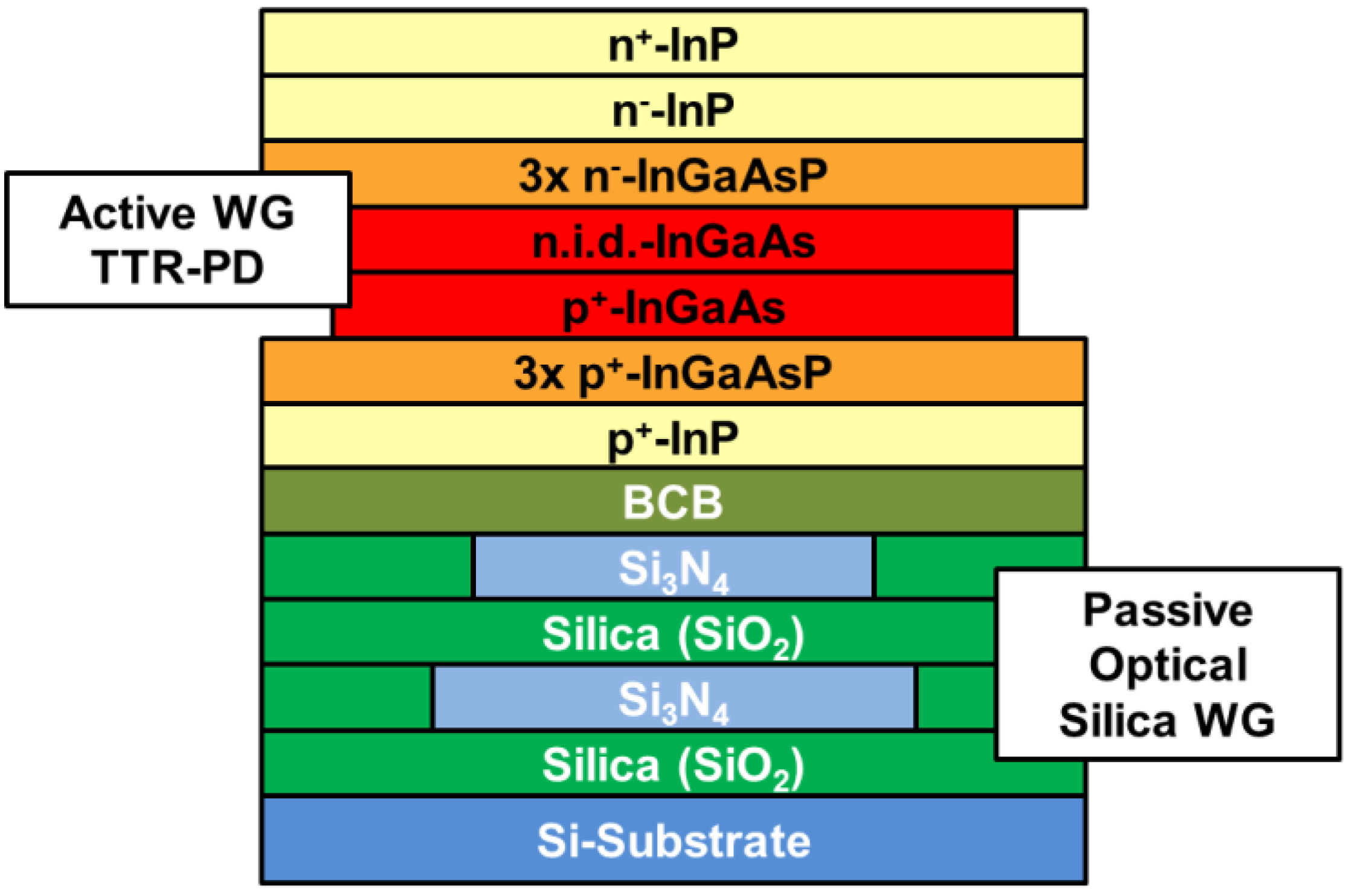
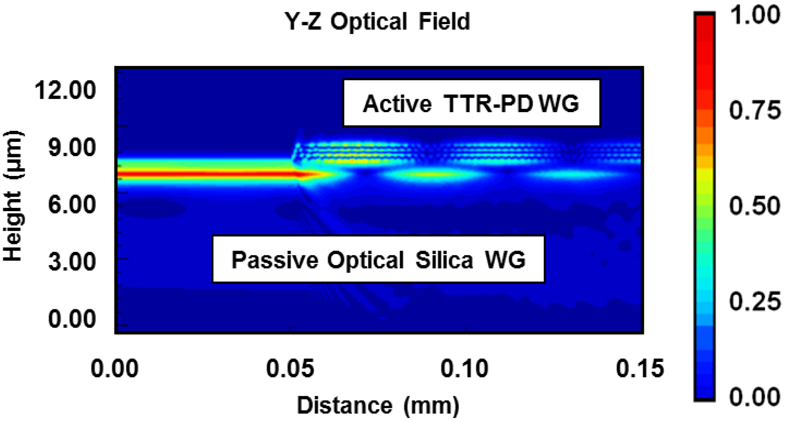
Prior to interfacing the TTR-PDs with integrated silica waveguides, the DC responsivity, the RF responsivity, the 3 dB bandwidth, and the 1 dB compression point of the developed TTR-PD structure were to be investigated. Based on the achieved BPM simulation results, several devices with an active TTR-PD area of 2 × 30 µm
2 were fabricated and experimentally characterized. To characterize the TTR-PDs, a monolithically-integrated passive optical InGaAsP/InP-based waveguide, providing a similar optical TE-mode profile with a mode field diameter (MFD) on the order of 1.5 μm [
21], was substituted for the silica waveguide in the layer structure design to enable (evanescent) optical coupling to the TTR-PD chip (see
Figure 5a). The top view of a fabricated TTR-PD chip is further shown in
Figure 5b. For on-chip measurements, no additional cooling arrangements, such as Peltier elements or heat sink modules, were applied to the TTR-PD chips. Further, it should be noted that no anti-reflection coating was deposited at the passive optical waveguide facets.
Figure 5.
(a) Schematic cross section of the TTR-PD layer structure with a monolithically-integrated passive optical waveguide (WG) and (b) scanning electron microscope (SEM) photograph of the fabricated WG TTR-PD chip.
Figure 5.
(a) Schematic cross section of the TTR-PD layer structure with a monolithically-integrated passive optical waveguide (WG) and (b) scanning electron microscope (SEM) photograph of the fabricated WG TTR-PD chip.
4.1. Polarization Behavior and DC Responsivity
To investigate the polarization behavior for optical heterodyne mmW signal generation (see
Section 4.2), the polarization dependent loss (PDL) of the TTR-PDs was measured within the complete optical C-band from 1530 to 1565 nm (see
Figure 6). The optical fiber-chip coupling to the passive optical waveguide was accomplished using a lensed SMF. The applied SMF featured a spot size diameter on the order of 1.7 µm to reduce the optical mode mismatch, which would be induced by using a standard SMF with an MFD of about 10.4 µm. For measuring the PDL, the optical input-power level was set to 10 dBm. Two direct current (DC) needle manipulators were used for biasing the TTR-PD chip at a bias voltage of −8 V. The measured PDL is plotted in
Figure 6.
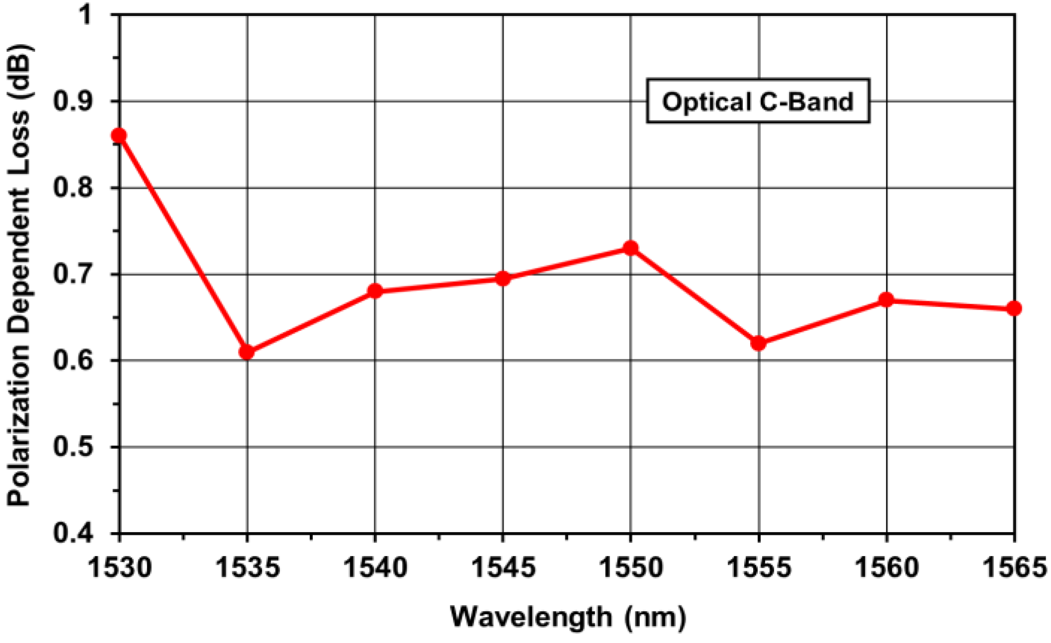
Figure 6.
Measured polarization dependent loss plotted against the optical wavelength for a bias voltage of −8 V.
Figure 6.
Measured polarization dependent loss plotted against the optical wavelength for a bias voltage of −8 V.
As can be seen from
Figure 6, within the entire C-band the TTR-PDs exhibit a reasonable PDL, which is less than 0.9 dB. A PDL of 0.73 dB can further be observed at the operational wavelength of 1.55 µm. In addition to that, a peak DC responsivity (R
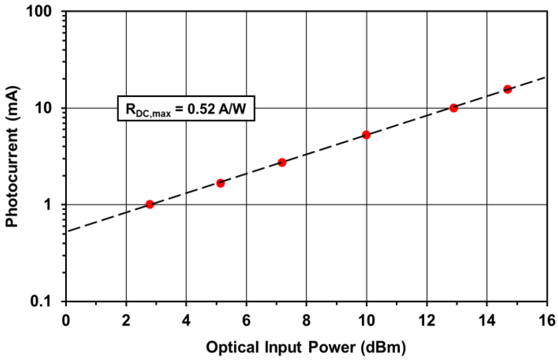
DC,max) on the order of 0.52 A/W was achieved (see
Figure 7).
Figure 7.
Measured photocurrent versus the optical input power for the operational wavelength of 1.55 µm at a bias voltage of −8 V. The dashed line shows the simulated photocurrent for the DC responsivity of 0.52 A/W.
Figure 7.
Measured photocurrent versus the optical input power for the operational wavelength of 1.55 µm at a bias voltage of −8 V. The dashed line shows the simulated photocurrent for the DC responsivity of 0.52 A/W.
4.2. Measured Frequency Response
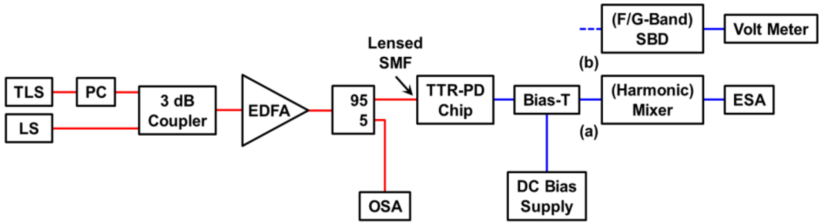
For measuring a frequency response from DC up to 220 GHz, we used a calibrated scalar network analyzer setup featuring a tunable external cavity laser (TLS) in conjunction with a polarization controller (PC) and a continuous wave laser source (LS) for optical heterodyne mmW signal generation. The measurement setup is illustrated in
Figure 8. Three different 100 µm pitch coplanar RF probes (~50 Ω) were used to attain on-chip power measurements within the measured frequency range shown in
Figure 9.
Figure 8.
Measurement setup based upon optical heterodyne millimeter wave signal generation up to 220 GHz featuring (a) an electrical spectrum analyzer (ESA) with internal and external mixers (DC–110 GHz) and (b) Schottky barrier diodes (SBDs) connected to a volt meter (90–220 GHz). An erbium-doped fiber amplifier (EDFA) and an optical spectrum analyzer (OSA) are further included in the setup.
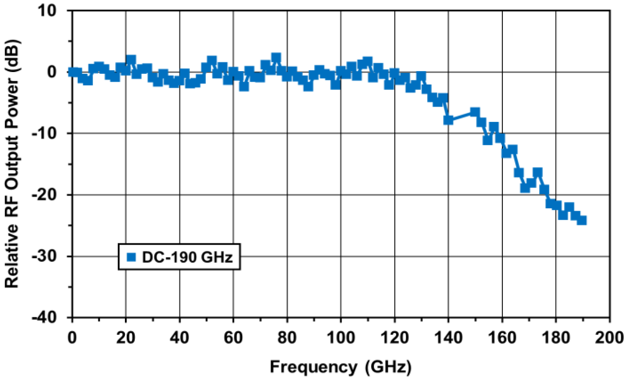
Up to a frequency of 110 GHz, an RF probe and an external bias-T, both including a 1 mm coaxial W1-connector, were applied together with an electrical spectrum analyzer (ESA) employing an internal mixer (up to 50 GHz) and the external V-band (50–75 GHz) and W-band (75–110 GHz) harmonic mixers. Within the frequency ranges of 90–140 GHz (F-band) and 140–220 GHz (G-band), two further RF probes featuring a WR-08 and a WR-05 waveguide output, respectively, and an integrated bias-T were used with corresponding Schottky barrier diodes (SBDs) and a volt meter. The measured frequency response up to 190 GHz is presented in
Figure 9. The photocurrent and the bias voltage of the TTR-PD were set to 1 mA and −8 V, respectively. From
Figure 9, one can notice that a 3 dB cut-off frequency of 132 GHz is achieved. The resulting RF responsivity is found to be on the order of 0.14 A/W. At lower frequencies, a maximum RF responsivity of about 0.24 A/W has been achieved.
Figure 9.
Measured relative RF output power from DC up to 190 GHz.
Figure 9.
Measured relative RF output power from DC up to 190 GHz.
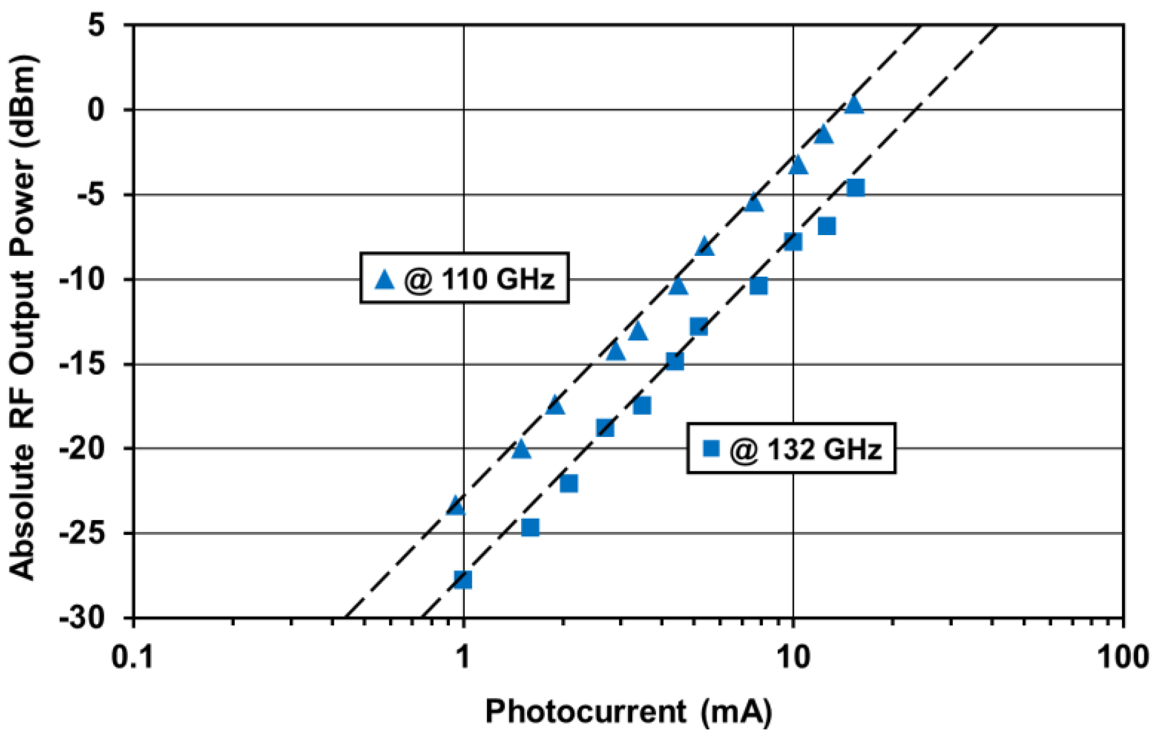
4.3. RF Output Power Measurements
Furthermore, the saturation effects were investigated within the 3 dB bandwidth. For calibrated power measurements at the 3 dB cut-off frequency (132 GHz), the F-band (90–140 GHz) SBD including an integrated WR-08 waveguide has been used together with a level set attenuator as the saturation of the SBDs starts at an RF input power of about −20 dBm. The maximum attenuation of the attenuator was set to 20 dB. Thus, the detected RF output power was measured for different optical input-power levels. In
Figure 10, the measured RF output power is plotted against the photocurrent for the bias voltage of −8 V.
Figure 10.
Measured RF output power plotted against the photocurrent for a bias voltage of −8 V at the frequencies of 110 GHz and 132 GHz. The dashed lines show the simulated output power for the RF responsivities of 0.24 A/W (110 GHz) and 0.14 A/W (132 GHz).
Figure 10.
Measured RF output power plotted against the photocurrent for a bias voltage of −8 V at the frequencies of 110 GHz and 132 GHz. The dashed lines show the simulated output power for the RF responsivities of 0.24 A/W (110 GHz) and 0.14 A/W (132 GHz).
As shown in
Figure 10, even at the 3 dB cut-off frequency no saturation effects occur and a maximum RF output power of −4.6 dBm is achieved, along with a photocurrent level of 15.5 mA. To identify the 1 dB compression point of the TTR-PD, a higher optical input-power level, which was not obtainable by the measurement setup, was required. However, the catastrophic optical damage of the passive optical waveguide facet caused by the applied lensed SMF has been calculated for an optical input-power level of about 24 dBm [
24]. Maximum RF output-power levels exceeding 0 dBm (e.g., at 110 GHz) were attained as can be seen from
Figure 10.
For hybrid integration of TTR-PDs on top of an optical silica waveguide, a limited number of modified TTR-PD chips have already been fabricated. Details will be reported elsewhere.
5. Conclusions
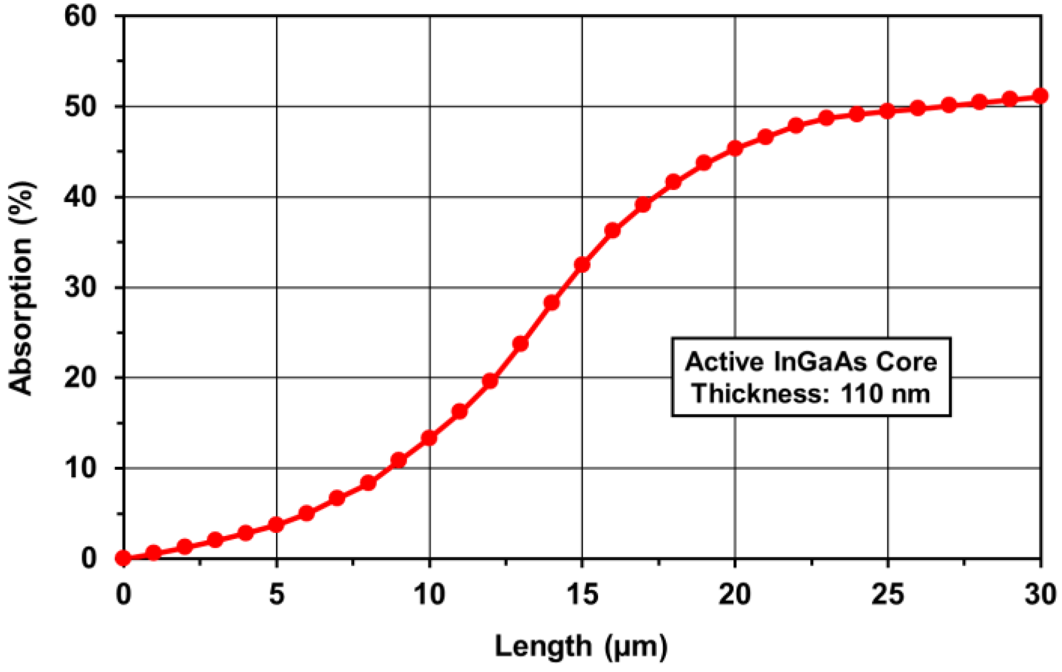
In this paper, we presented a novel high-speed InP-based waveguide triple transit region photodiode (TTR-PD) structure for hybrid integration with passive optical silica waveguides, which are fundamental to form an optical beam-steering network. As an application for future 5G mobile systems, we proposed a scheme for a hybrid-integrated InP/silicon-based photonic millimeter wave transmitter, enabling photonic RF beam forming and beam steering. For this approach, the TTR-PD chip was integrated on top of a passive optical silica waveguide to achieve evanescent optical coupling. Numerical beam propagation method analyses revealed that a coupling efficiency of around 90% is attained between a passive silica waveguide and the active InP-based waveguide TTR-PD, as well as an absorption of about 50% within a simulated TTR-PD length of 30 µm. For fabricated TTR-PD chips including a monolithically-integrated passive optical waveguide, a reasonable polarization dependent loss of less than 0.9 dB was achieved within the optical C-band (e.g., 0.73 dB at 1.55 µm). Moreover, a 3 dB cut-off frequency of 132 GHz was experimentally demonstrated. Within the 3 dB bandwidth, RF output-power levels higher than 0 dBm were measured for the fabricated TTR-PDs. The DC responsivity and the RF responsivity were found to be on the order of 0.52 A/W and 0.24 A/W, respectively.


