Wide Spectral Characteristics of Si Photonic Crystal Mach-Zehnder Modulator Fabricated by Complementary Metal-Oxide-Semiconductor Process


Abstract
:
1. Introduction
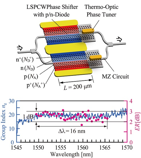
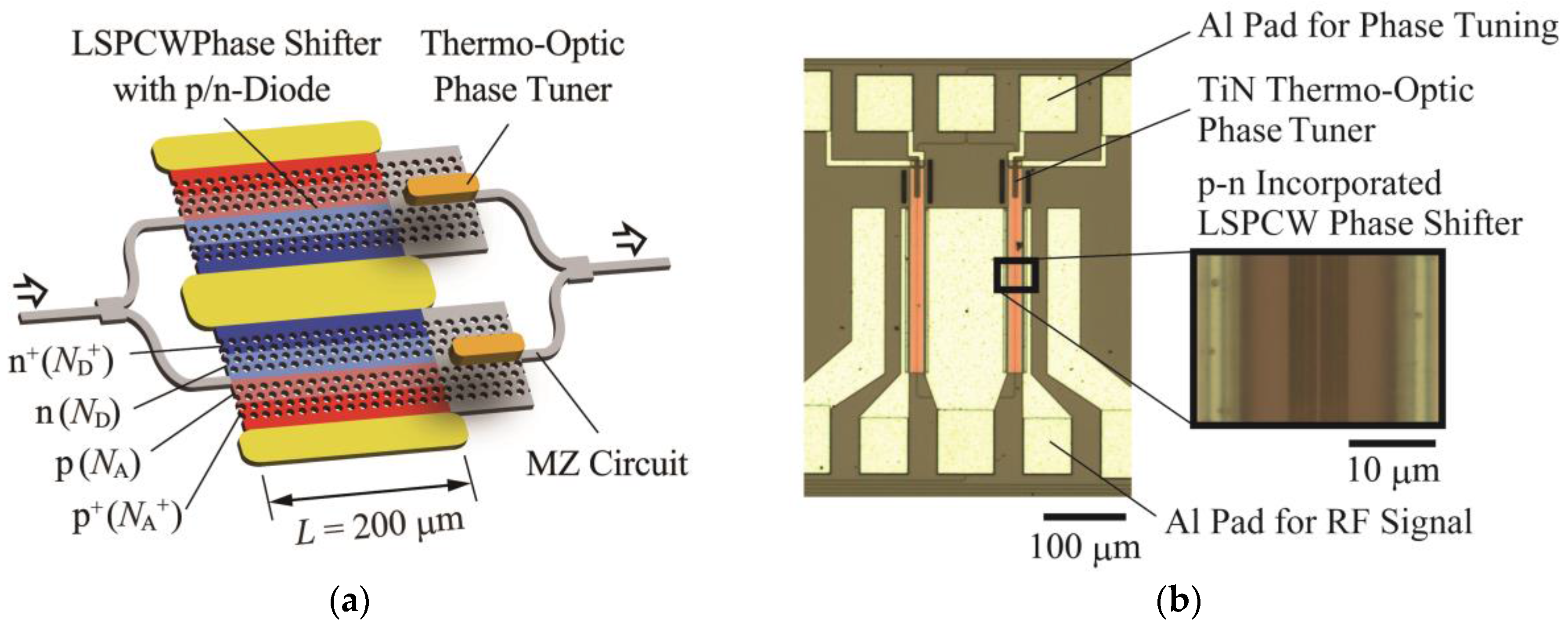
2. Device
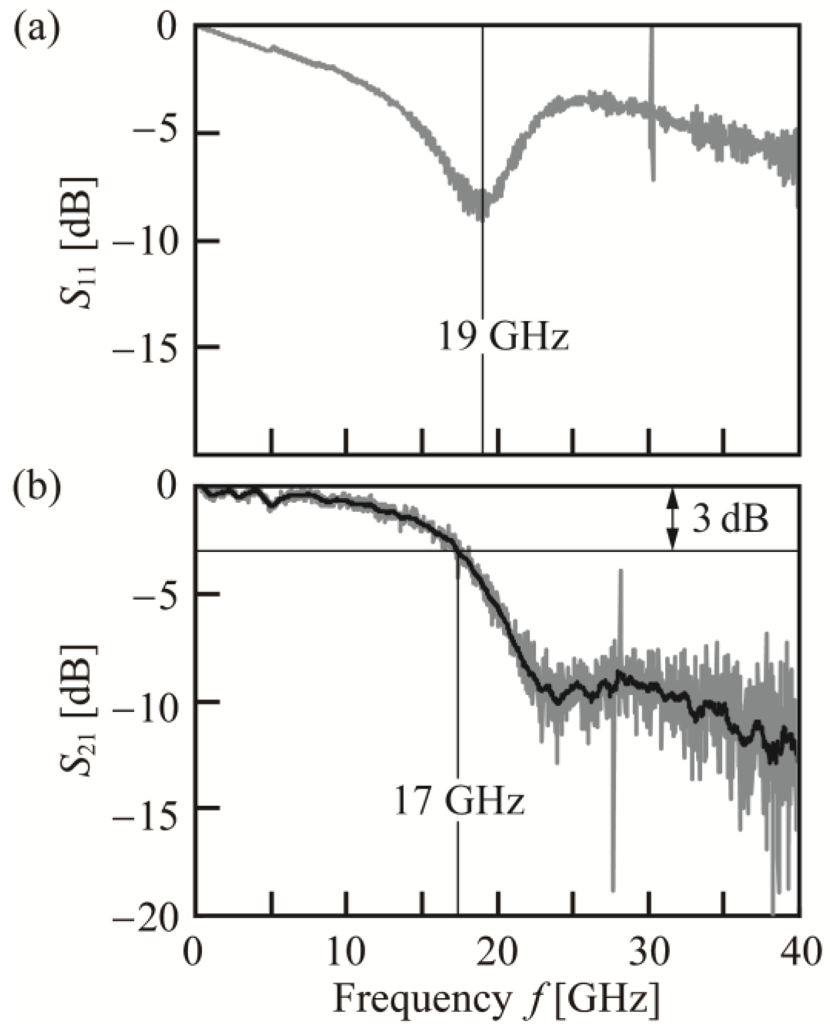
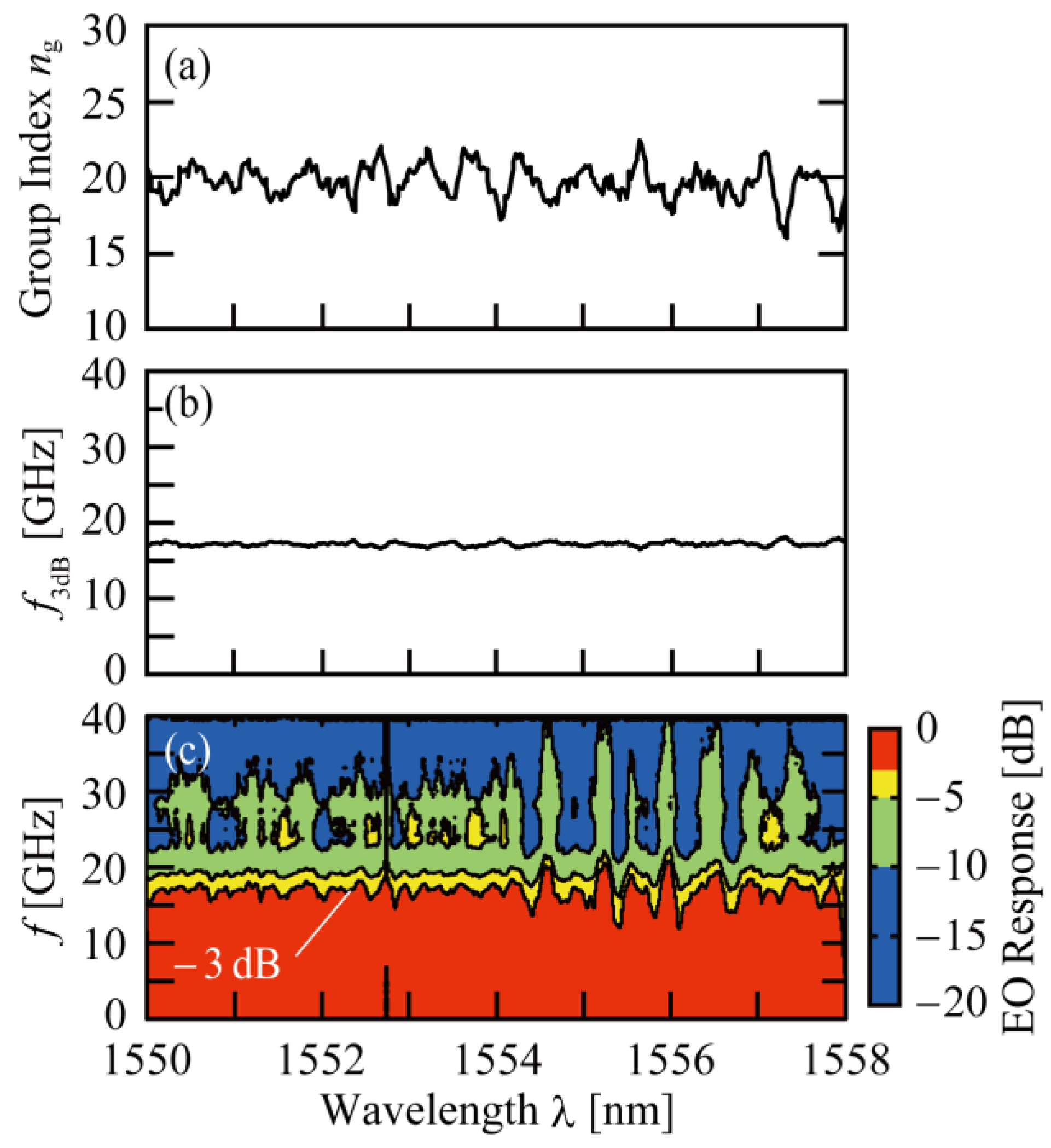
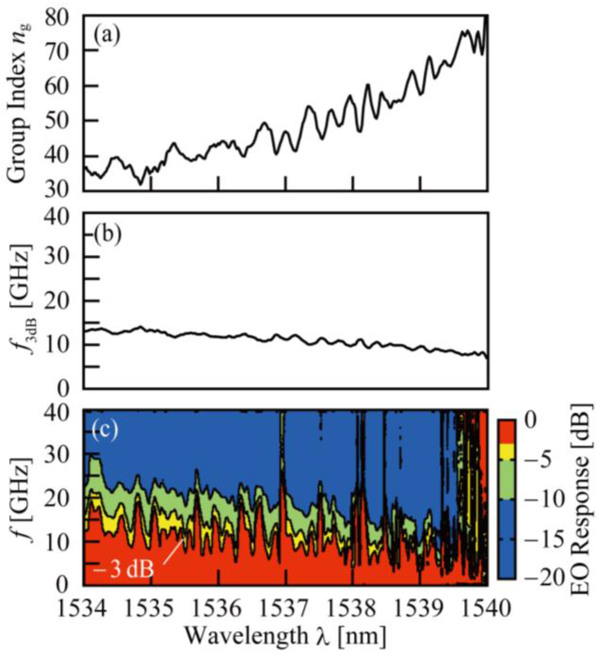
3. Frequency Response
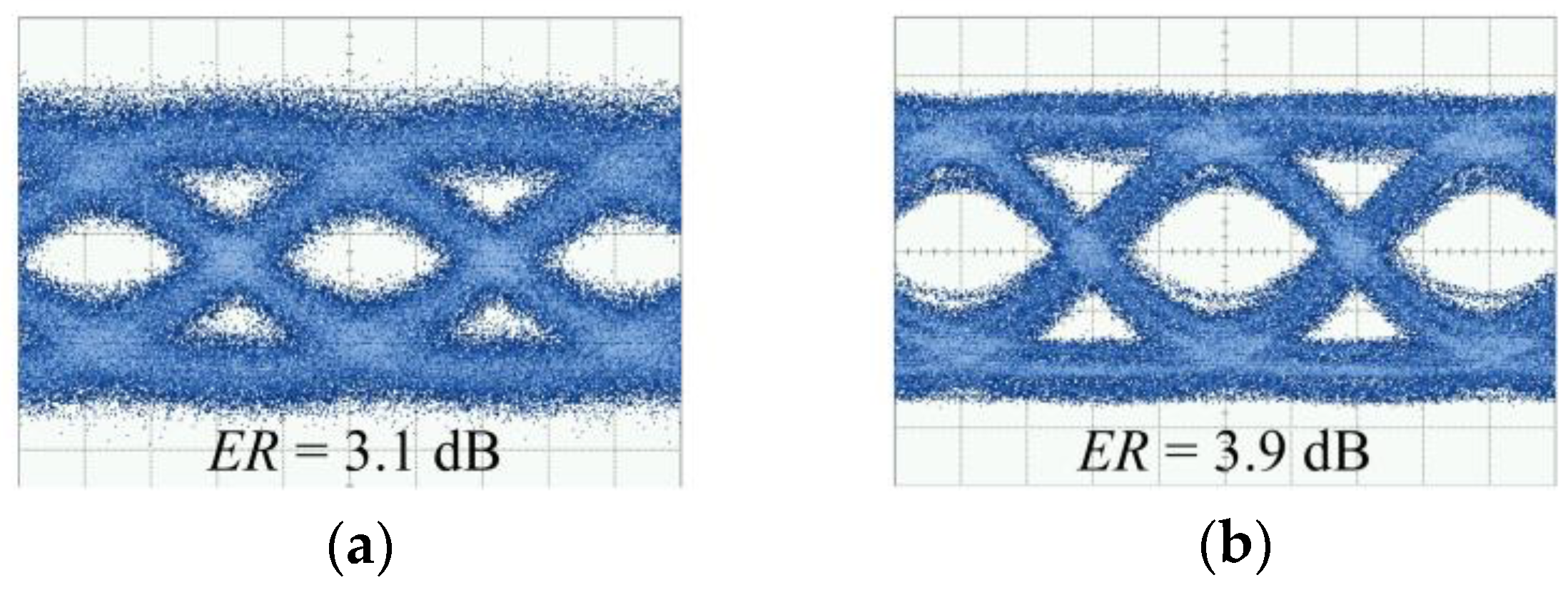
4. Signal Modulation
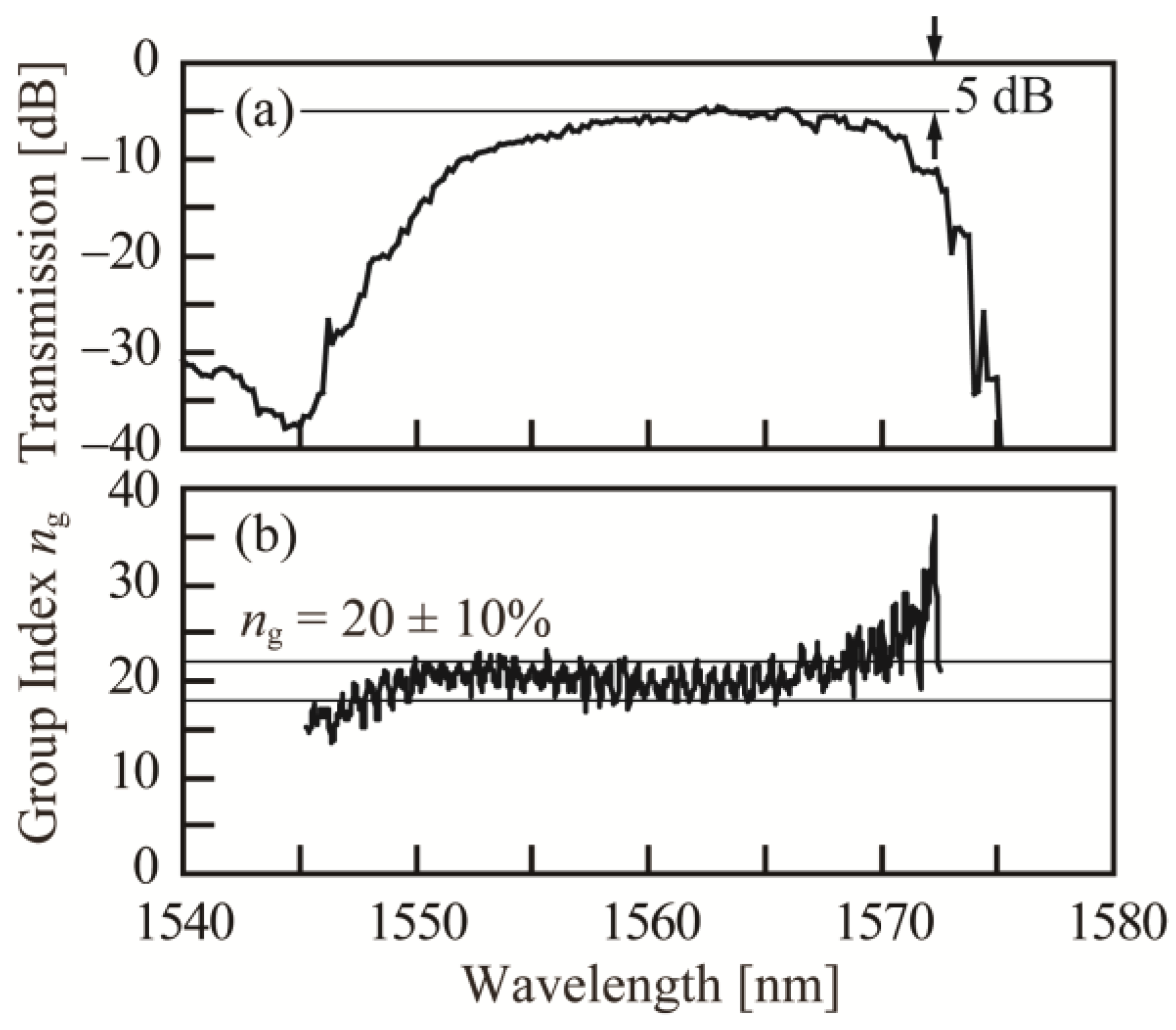
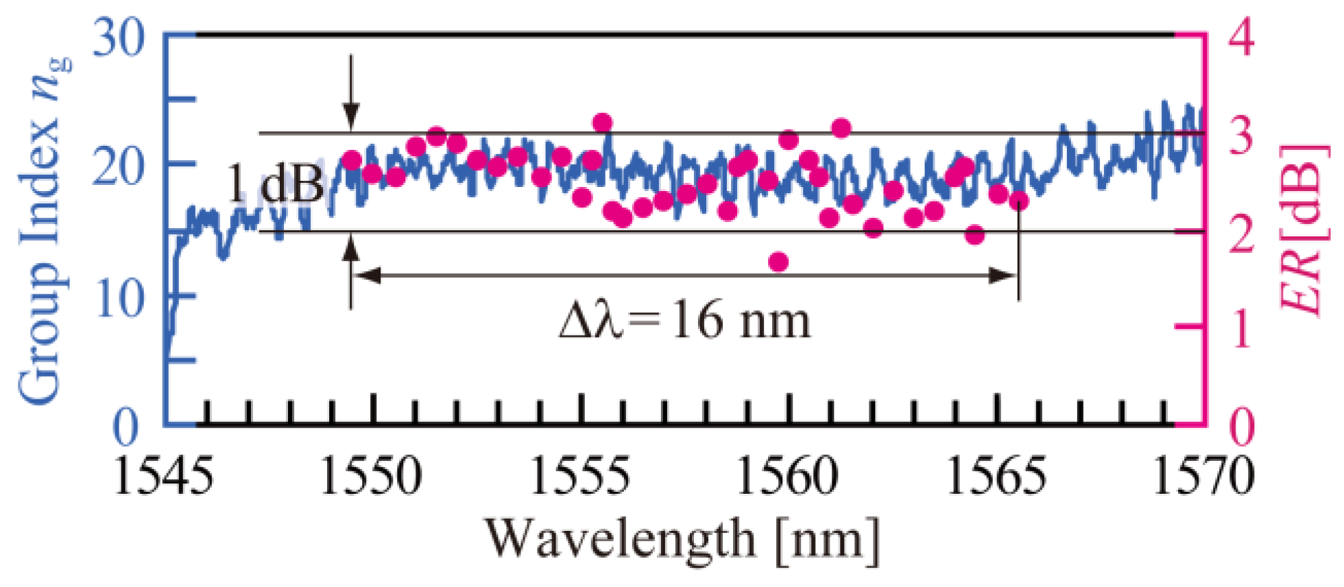
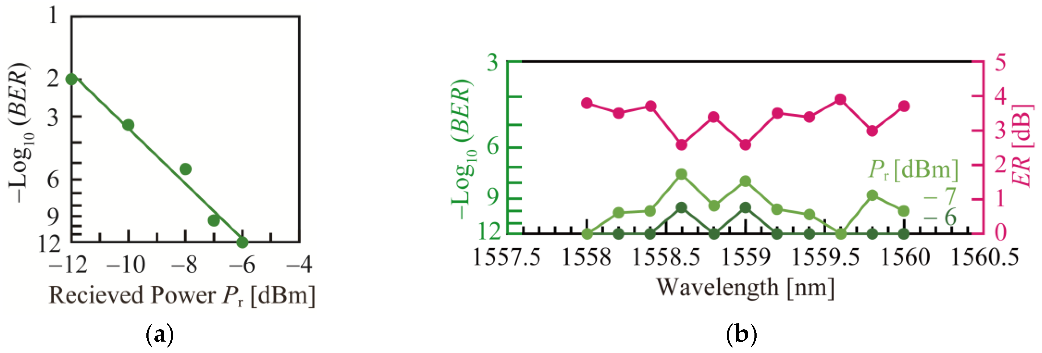
5. Slow-Light Enhancement
6. Conclusions
Acknowledgments
Author Contributions
Conflicts of Interest
References
- Reed, G.T.; Mashanovich, G.; Gardes, F.Y.; Thomson, D.J. Silicon optical modulators. Nat. Photonics 2010, 4, 518–526. [Google Scholar] [CrossRef] [Green Version]
- Thomson, D.J.; Gardes, F.Y.; Fedeli, J.M.; Zlatanovic, S.; Hu, Y.; Kuo, B.P.P.; Myslivets, E.; Alic, N.; Radic, S.; Mashanovich, G.Z.; et al. 50-Gb/s silicon optical modulator. IEEE Photonics Technol. Lett. 2012, 24, 234–236. [Google Scholar] [CrossRef]
- Yang, L.; Ding, J. High-speed silicon Mach-Zehnder optical modulator with large optical bandwidth. J. Lightwave Technol. 2014, 32, 966–970. [Google Scholar] [CrossRef]
- Xu, H.; Li, X.; Xiao, X.; Li, Z.; Yu, Y.; Yu, J. Demonstration and characterization of high-speed silicon depletion-mode Mach-Zehnder modulators. IEEE J. Sel. Top. Quantum Electron. 2014, 20, 23–32. [Google Scholar] [CrossRef]
- Akiyama, S.; Imai, M.; Baba, T.; Akagawa, T.; Hirayama, N.; Noguchi, Y.; Seki, M.; Koshino, K.; Toyama, M.; Horikawa, T.; et al. Compact PIN-diode-based silicon modulator using side-wall-grating waveguide. IEEE J. Sel. Top. Quantum Electron. 2013, 19, 74–84. [Google Scholar] [CrossRef]
- Ding, R.; Liu, Y.; Ma, Y.; Yang, Y.; Li, Q.; Lim, A.E.J.; Lo, G.Q.; Bergman, K.; Baehr-Jones, T.; Hochberg, M. High-speed silicon modulator with slow-wave electrodes and fully independent differential drive. J. Lightwave Technol. 2014, 32, 2240–2247. [Google Scholar] [CrossRef]
- Timurdogan, E.; Sorace-Agaskar, C.M.; Sun, J.; Hosseini, E.S.; Biberman, A.; Watts, M.R. An ultralow power athermal silicon modulator. Nat. Commun. 2014, 5, 4008. [Google Scholar] [CrossRef] [PubMed]
- Zheng, X.; Chang, E.; Amberg, P.; Shubin, I.; Lexau, J.; Liu, F.; Thacker, H.; Djordjevic, S.S.; Lin, S.; Luo, Y.; et al. A high-speed, tunable silicon Photonic ring modulator integrated with ultra-efficient active wavelength control. Opt. Express 2014, 22, 12628–12633. [Google Scholar] [CrossRef] [PubMed]
- Sun, C.; Wade, M.T.; Lee, Y.; Orcutt, J.S.; Alloatti, L.; Georgas, M.S.; Waterman, A.S.; Shainline, J.M.; Avizienis, R.R.; Lin, S.; et al. Single-chip microprocessor that communicates directly using light. Nature 2015, 528, 534–538. [Google Scholar] [CrossRef] [PubMed]
- Tamura, T.; Kondo, K.; Terada, Y.; Hinakura, Y.; Ishikura, N.; Baba, T. Silica-Clad Silicon Photonic Crystal Waveguides for Wideband Dispersion-Free Slow Light. J. Lightwave Technol. 2015, 33, 3034–3040. [Google Scholar] [CrossRef]
- Nguyen, H.C.; Sakai, Y.; Shinkawa, M.; Ishikura, N.; Baba, T. 10 Gb/s operation of photonic crystal silicon optical modulators. Opt. Express 2011, 19, 13000–13007. [Google Scholar] [CrossRef] [PubMed]
- Nguyen, H.C.; Sakai, Y.; Shinkawa, M.; Ishikura, N.; Baba, T. Photonic crystal silicon optical modulators: Carrier-injection and depletion at 10 Gb/s. IEEE J. Quantum Electron. 2012, 48, 210–220. [Google Scholar] [CrossRef]
- Nguyen, H.C.; Hashimoto, S.; Shinkawa, M.; Baba, T. Compact and fast photonic crystal silicon optical modulators. Opt. Express 2012, 20, 22465–22474. [Google Scholar] [CrossRef] [PubMed]
- Nguyen, H.C.; Yazawa, N.; Hashimoto, S.; Otsuka, S.; Baba, T. Sub-100 μm photonic crystal Si optical modulators: Spectral, athermal, and high-speed performance. IEEE J. Sel. Top Quantum Electron. 2013, 19, 127–137. [Google Scholar] [CrossRef]
- Terada, Y.; Ito, H.; Nguyen, H.C.; Baba, T. Theoretical and experimental investigation of low-voltage and low-loss 25-Gbps Si photonic crystal slow light Mach-Zehnder modulators with interleaved p/n junction. Front. Phys. 2014, 2, 1–9. [Google Scholar] [CrossRef]
- Brosi, J.M.; Koos, C.; Andreani, L.C.; Waldow, M.; Leuthold, J.; Freude, W. High-speed low-voltage electro-optic modulator with a polymer-infiltrated silicon photonic crystal waveguide. Opt. Express 2008, 16, 4177–4191. [Google Scholar] [CrossRef] [PubMed]
- O’Faolain, L.; Schulz, S.A.; Beggs, D.M.; White, T.P.; Spasenović, M.; Kuipers, L.; Morichetti, F.; Melloni, A.; Mazoyer, S.; Hugonin, J.P.; et al. Loss engineered slow light waveguides. Opt. Express 2010, 18, 27627–27638. [Google Scholar] [CrossRef] [PubMed] [Green Version]
- Ponchak, G.E.; Papapolymerou, J.; Tentzeris, M.M. Excitation of coupled slotline mode in finite-ground CPW with unequal ground-plane widths. IEEE Trans. Microwave Theory Technol. 2005, 53, 713–717. [Google Scholar] [CrossRef]
- Shin, J.H.; Sakamoto, S.R.; Dagli, N. Conductor loss of capacitively loaded slow wave electrodes for high-speed photonic devices. J. Lightwave Technol. 2011, 29, 48–52. [Google Scholar] [CrossRef]
- Chen, H.W.; Kuo, Y.H.; Bowers, J.E. 25 Gb/s hybrid silicon switch using a capacitively loaded traveling wave electrode. Opt. Express 2010, 18, 1070–1075. [Google Scholar] [CrossRef] [PubMed]
- Li, G.L.; Mason, T.G.B.; Yu, P.K.L. Analysis of segmented traveling-wave optical modulators. J. Lightwave Technol. 2004, 22, 1789–1796. [Google Scholar] [CrossRef]
- Jaeger, N.A.; Lee, Z.K. Slow-wave electrode for use in compound semiconductor electrooptic modulators. IEEE J. Quantum Electron. 1992, 28, 1778–1784. [Google Scholar] [CrossRef]


© 2016 by the authors; licensee MDPI, Basel, Switzerland. This article is an open access article distributed under the terms and conditions of the Creative Commons by Attribution (CC-BY) license (http://creativecommons.org/licenses/by/4.0/).
Share and Cite
Hinakura, Y.; Terada, Y.; Tamura, T.; Baba, T. Wide Spectral Characteristics of Si Photonic Crystal Mach-Zehnder Modulator Fabricated by Complementary Metal-Oxide-Semiconductor Process. Photonics 2016, 3, 17. https://doi.org/10.3390/photonics3020017
Hinakura Y, Terada Y, Tamura T, Baba T. Wide Spectral Characteristics of Si Photonic Crystal Mach-Zehnder Modulator Fabricated by Complementary Metal-Oxide-Semiconductor Process. Photonics. 2016; 3(2):17. https://doi.org/10.3390/photonics3020017
Chicago/Turabian StyleHinakura, Yosuke, Yosuke Terada, Takuya Tamura, and Toshihiko Baba. 2016. "Wide Spectral Characteristics of Si Photonic Crystal Mach-Zehnder Modulator Fabricated by Complementary Metal-Oxide-Semiconductor Process" Photonics 3, no. 2: 17. https://doi.org/10.3390/photonics3020017