Integration of Single-Photon Sources and Detectors on GaAs

Abstract
:1. Introduction
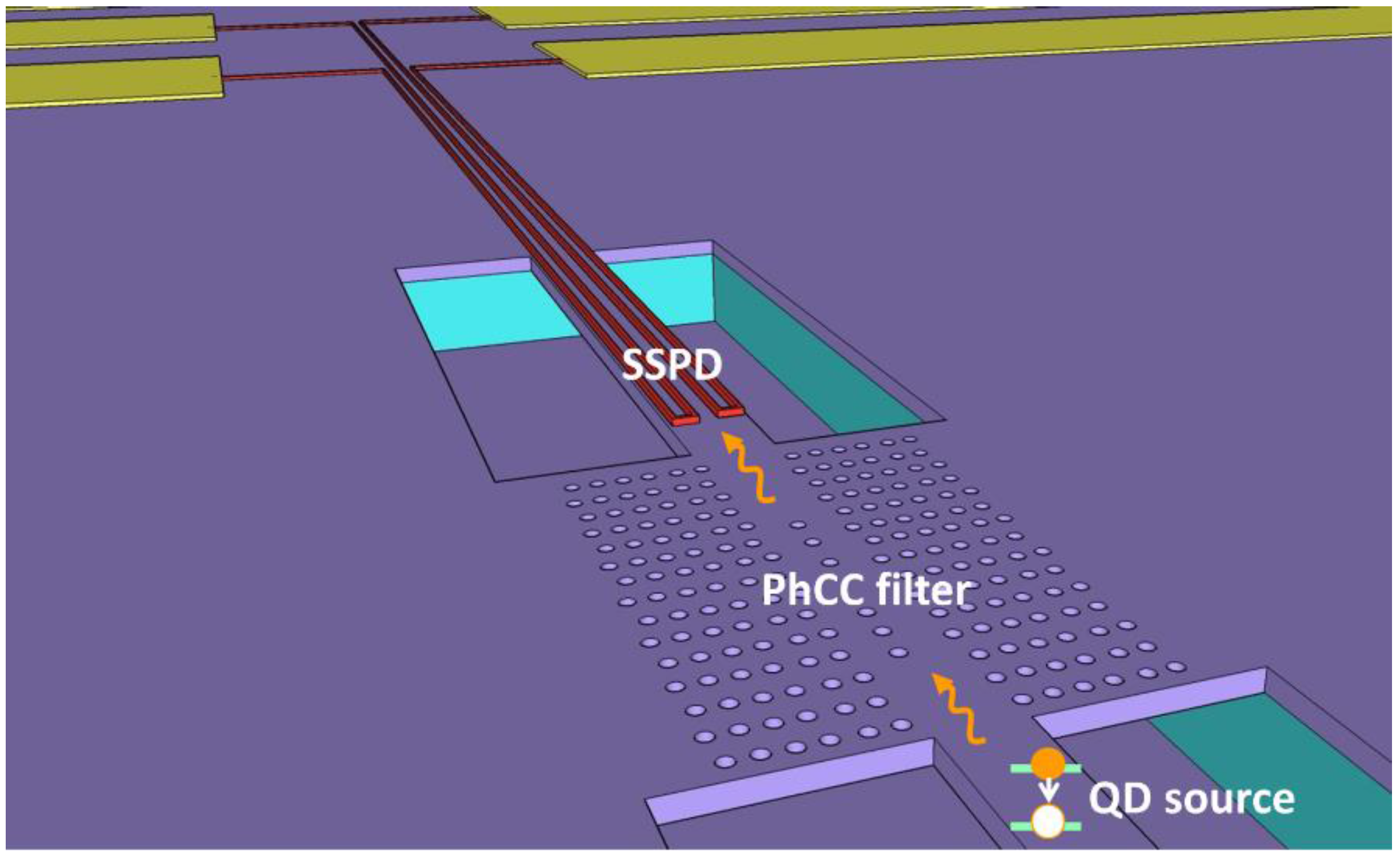
2. Materials and Methods
3. Results
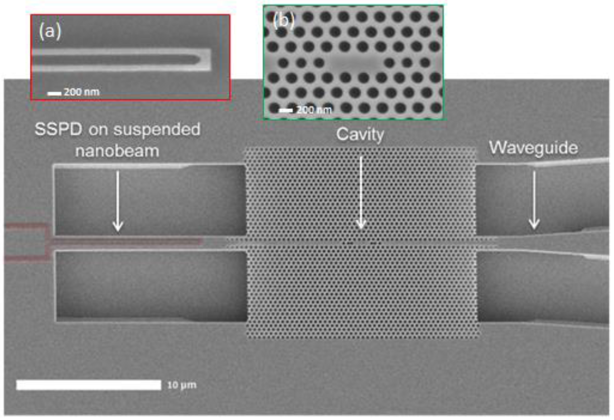
3.1. Detectors
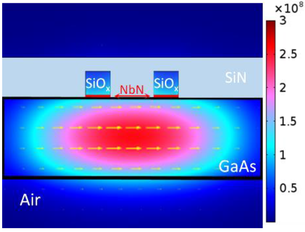
3.1.1. Design
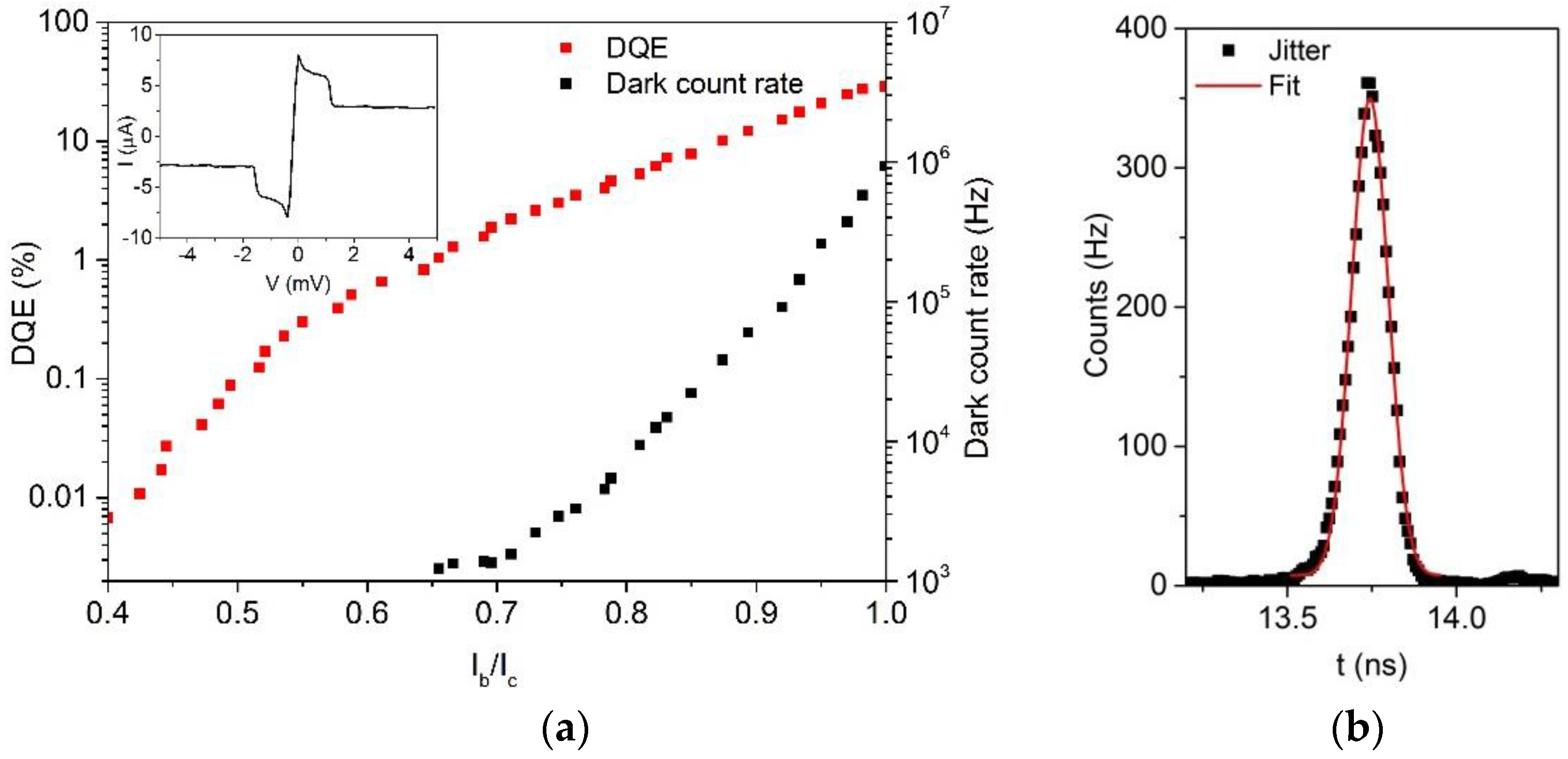
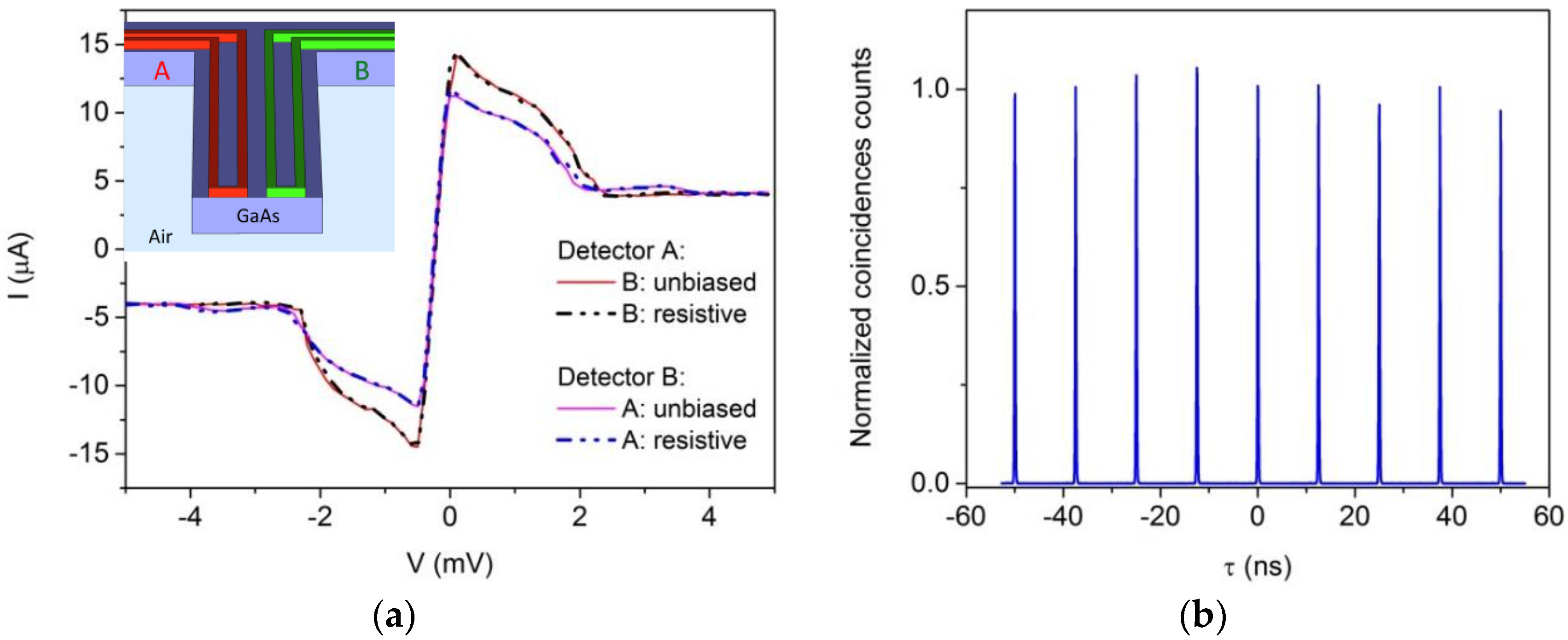
3.1.2. Performance
3.1.3. Autocorrelator Performance
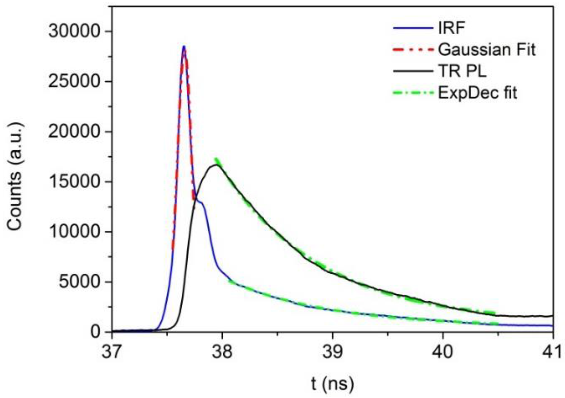
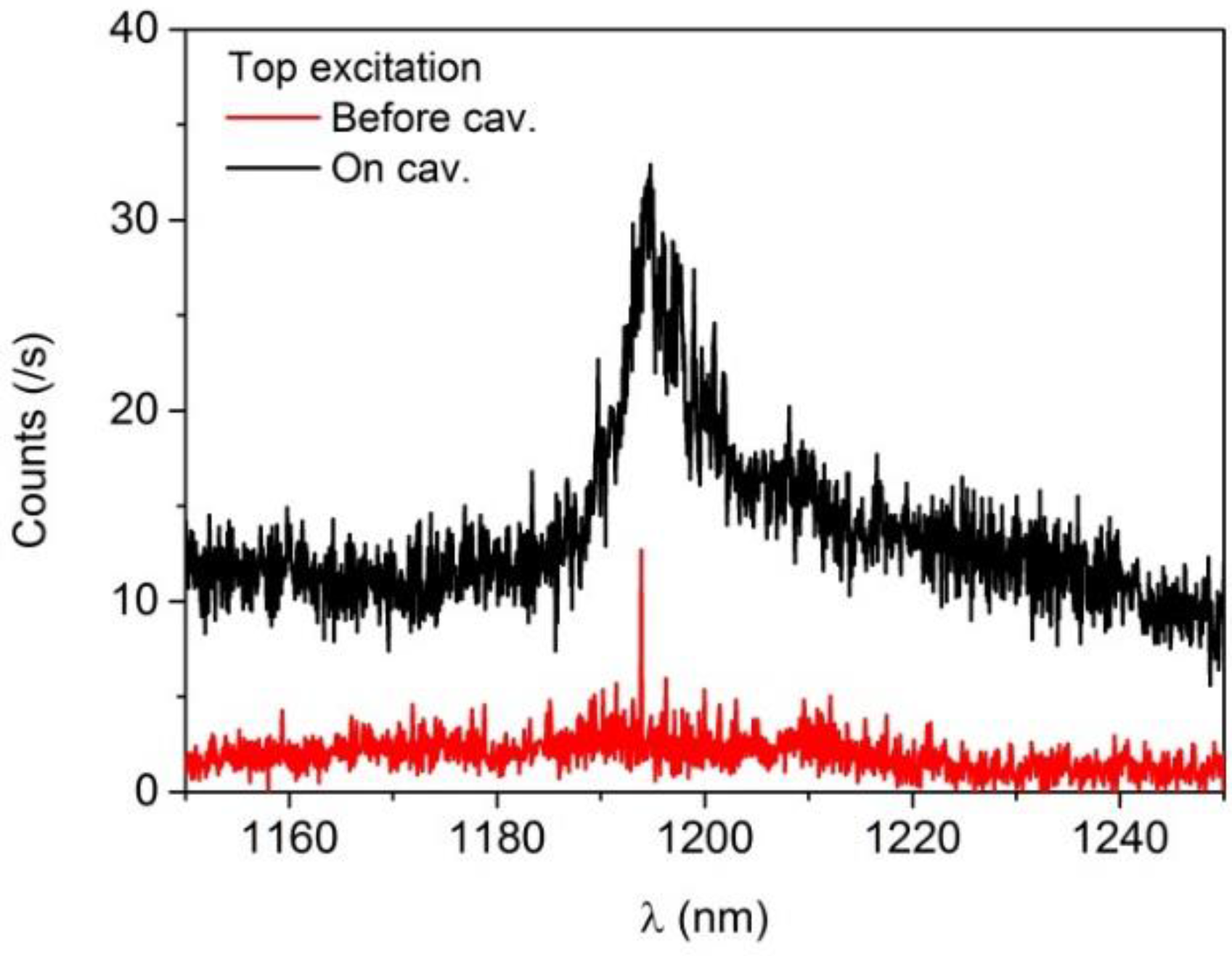
3.2. QD Emission
On-Chip Detection
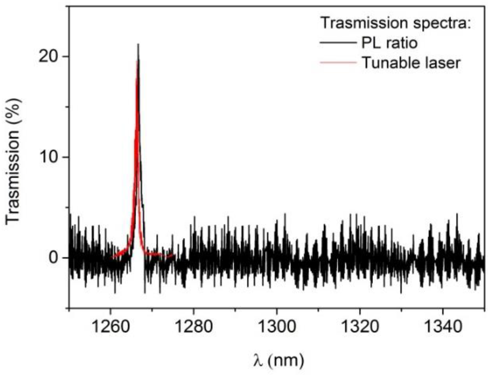
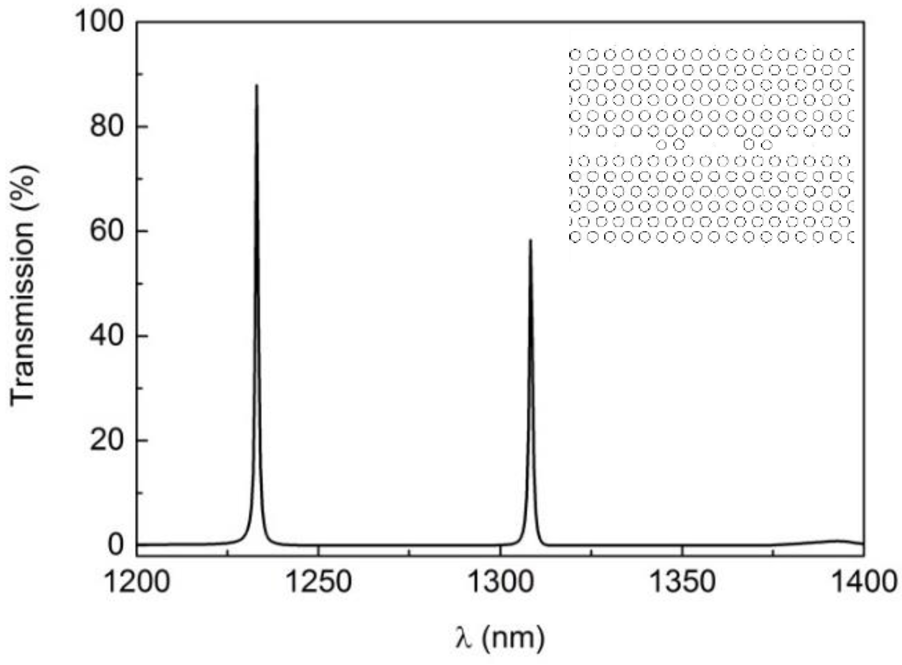
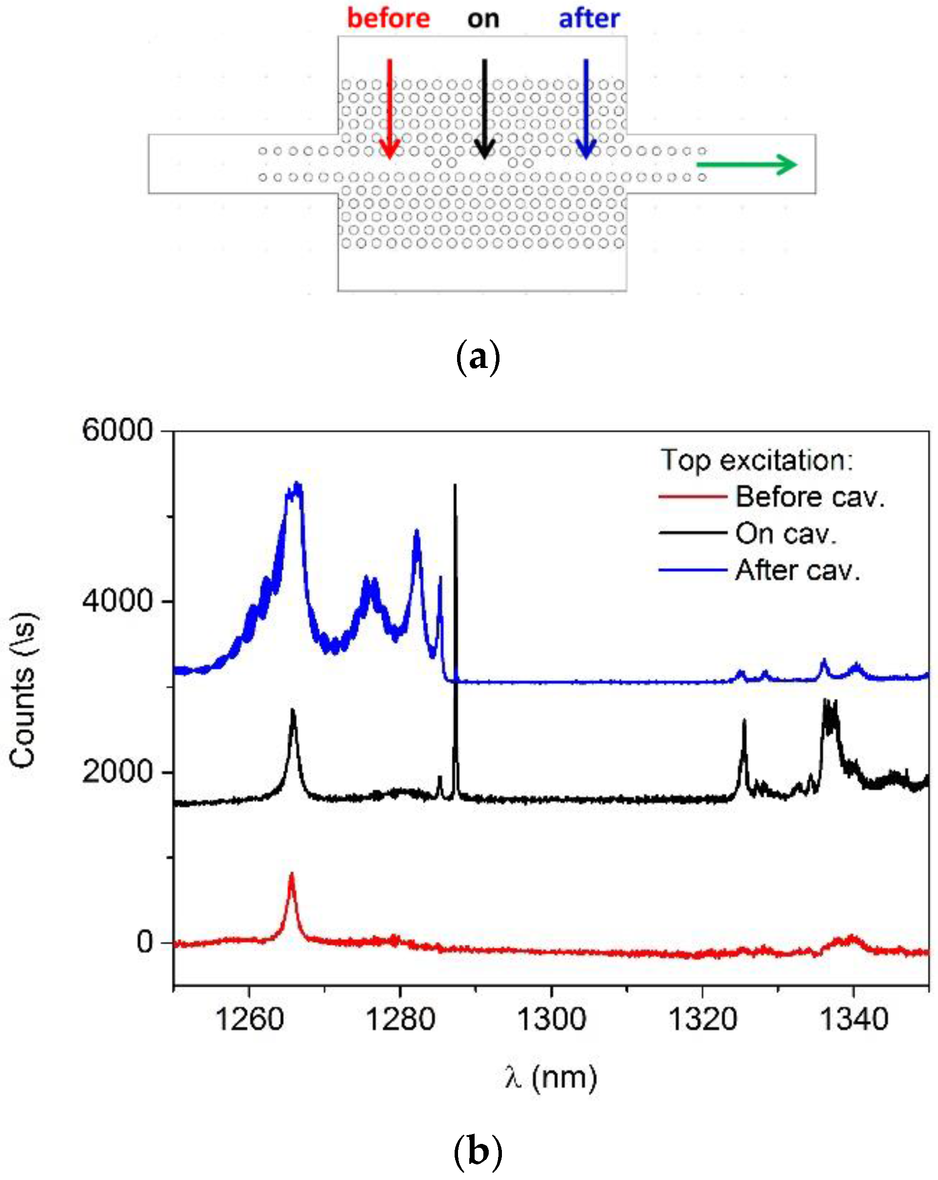
3.3. Filters
3.3.1. Design
3.3.2. Performance
3.3.3. Filtering of Single QD Lines
4. Discussion
Acknowledgments
Author Contributions
Conflicts of Interest
References
- O’Brien, J.L. Optical quantum computing. Science 2007, 318, 1567–1570. [Google Scholar] [CrossRef] [PubMed]
- O’Brien, J.L.; Fusawa, A.; Vuckovic, J. Photonic quantum technologies. Nat. Phys. 2009, 3, 687–695. [Google Scholar] [CrossRef]
- Dietrich, C.P.; Fiore, A.; Thompson, M.G.; Kamp, M.; Hofling, S. GaAs integrated quantum photonics: Towards compact and multi-functional quantum photonic integrated circuits. 2016. [Google Scholar]
- Shields, A.J. Semiconductor quantum light sources. Nat. Photonics 2007, 1, 215–223. [Google Scholar] [CrossRef]
- Englund, D.; Faraon, A.; Zhang, B.; Yamamoto, Y.; Vucković, J. Generation and transfer of single photons on a photonic crystal chip. Opt. Express 2007, 15, 5550–5558. [Google Scholar] [CrossRef] [PubMed]
- Schwagmann, A.; Kalliakos, S.; Farrer, I.; Griffiths, J.P.; Jones, G.A.C.; Ritchie, D.A.; Shields, A.J. On-chip single photon emission from an integrated semiconductor quantum dot into a photonic crystal waveguide. Appl. Phys. Lett. 2011, 99, 261108. [Google Scholar] [CrossRef]
- Laucht, A.; Pütz, S.; Günthner, T.; Hauke, N.; Saive, R.; Frédérick, S.; Bichler, M.; Amann, M.-C.; Holleitner, A.W.; Kaniber, M.; et al. A waveguide-coupled on-chip single-photon source. Phys. Rev. X 2012, 2, 011014. [Google Scholar] [CrossRef]
- Hoang, T.B.; Midolo, L.; Dietrich, C.P.; Li, L.H.; Linfield, E.H.; Schouwenberg, J.F.P.; Xia, T.; Pagliano, F.M.; van Otten, F.W.M.; Fiore, A. Efficient coupling of single photons to ridge-waveguide photonic integrated circuits. Appl. Phys. Lett. 2013, 102, 131105. [Google Scholar]
- Tanzilli, S.; de Riedmatten, H.; Zbinden, H.; Baldi, P.; de Micheli, M.; Ostrowsky, D.; Gisin, N. Highly efficient photon-pair source using periodically poled lithium niobate waveguide. Electron. Lett. 2001, 37, 26–28. [Google Scholar] [CrossRef] [Green Version]
- Sharping, J.E.; Lee, K.F.; Foster, M.A.; Turner, A.C.; Schmidt, B.S.; Lipson, M.; Gaeta, A.L.; Kumar, P. Generation of correlated photons in nanoscale silicon waveguides. Opt. Express 2006, 14, 12388–12393. [Google Scholar] [CrossRef] [PubMed]
- Patel, R.B.; Bennett, A.J.; Farrer, I.; Nicoll, C.A.; Shields, A.J. Two-photon interference of the emission from electrically tunable remote quantum dots. Nat. Photonics 2010, 4, 632–635. [Google Scholar] [CrossRef]
- Hoang, T.B.; Beetz, J.; Lermer, M.; Midolo, L.; Kamp, M.; Höfling, S.; Fiore, A. Widely tunable, efficient on-chip single photon sources at telecommunication wavelengths. Opt. Express 2012, 20, 21758–21765. [Google Scholar] [CrossRef] [PubMed]
- Midolo, L.; Pagliano, F.; Hoang, T.B.; Xia, T.; van Otten, F.W.M.; Li, L.H.; Linfield, E.H.; Lermer, M.; Hofling, S.; Fiore, A. Spontaneous emission control of single quantum dots by electromechanical tuning of a photonic crystal cavity. Appl. Phys. Lett. 2012, 101, 091106. [Google Scholar] [CrossRef]
- Petruzzella, M.; Xia, T.; Pagliano, F.; Birindelli, S.; Midolo, L.; Zobenica, Z.; Li, L.H.; Linfield, E.H.; Fiore, A. Fully tuneable, Purcell-enhanced solid-state quantum emitters. Appl. Phys. Lett. 2015, 107, 141109. [Google Scholar] [CrossRef]
- Gol’tsman, G.N.; Okunev, O.; Chulkova, G.; Lipatov, A.; Semenov, A.; Smirnov, K.; Voronov, B.; Dzardanov, A.; Williams, C.; Sobolewski, R. Picosecond superconducting single-photon optical detector. Appl. Phys. Lett. 2001, 79, 705–707. [Google Scholar] [CrossRef]
- Natarajan, C.M.; Tanner, M.G.; Hadfield, R.H. Superconducting nanowire single-photon detectors: Physic and application. Supercond. Sci. Technol. 2012, 25, 063001. [Google Scholar] [CrossRef]
- Sprengers, J.; Gaggero, A.; Sahin, D.; Jahanmirinejad, S.; Frucci, G.; Mattioli, F.; Leoni, R.; Beetz, J.; Lermer, M.; Kamp, M.; et al. Waveguide superconducting single-photon detectors for integrated quantum photonic circuits. Appl. Phys. Lett. 2011, 99, 181110. [Google Scholar] [CrossRef]
- Kaniber, M.; Flassig, F.; Reithmaier, G.; Gross, R.; Finley, J.J. Integrated superconducting detectors on semiconductors for quantum optics application. Appl. Phys. B 2016, 22, 1–10. [Google Scholar] [CrossRef]
- Pernice, W.H.P.; Schuck, C.; Minaeva, O.; Li, M.; Goltsman, G.N.; Sergienko, A.V.; Than, H.X. High-speed and high-efficiency travelling wave single-photon detectors embedded in nanophotonic circuits. Nat. Commun. 2012, 3, 1325. [Google Scholar] [CrossRef] [PubMed]
- Akhlaghi, M.K.; Schelew, E.; Young, J.F. Waveguide integrated superconducting single photon detectors implemented as coherent perfect absorbers. 2014. [Google Scholar]
- Sahin, D.; Gaggero, A.; Weber, J.W.; Agafonov, I.; Verheijen, M.A.; Mattioli, F.; Beetz, J.; Kamp, M.; Höfling, S.; van de Sanden, M.C.M.; et al. Waveguide nanowire superconducting single-photon detectors fabricated on GaAs and the study of their optical properties. IEEE J. Sel. Top. Quant. Electron. 2015, 21, 1–10. [Google Scholar] [CrossRef]
- Gaudio, R.; Op’t Hoog, K.P.M.; Zhou, Z.; Sahin, D.; Fiore, A. Inhomogeneous critical current in nanowire superconducting single-photon detectors. Appl. Phys. Lett. 2014, 105, 222602. [Google Scholar] [CrossRef]
- Sahin, D.; Gaggero, A.; Hoang, T.B.; Frucci, G.; Mattioli, F.; Leoni, R.; Beetz, J.; Lermer, M.; Kamp, M.; Höfling, S.; Fiore, A. Integrated autocorrelator based on superconducting nanowires. Opt. Express 2013, 21, 11162–11170. [Google Scholar] [CrossRef] [PubMed]
- Brown, R.H.; Twiss, R. A test of a new type of stellar interferometer on Sirius. Nature 1956, 178, 1046–1048. [Google Scholar] [CrossRef]
- Gaggero, A.; Nejad, S.J.; Marsili, F.; Mattioli, F.; Leoni, R.; Bitauld, D.; Sahin, D.; Hamhuis, G.J.; Nötzel, R.; Sanjines, R.; et al. Nanowire superconducting single-photon detectors on GaAs for integrated quantum photonic applications. Appl. Phys. Lett. 2010, 97, 151108. [Google Scholar] [CrossRef]
- Li, L.H.; Chauvin, N.; Patriarche, G.; Alloing, B.; Fiore, A. Growth-interruption-induced low-density InAs quantum dots on GaAs. J. Appl. Phys. 2008, 104, 083508. [Google Scholar] [CrossRef]
- Clem, J.R.; Berggren, K.K. Geometry-dependent critical currents in superconducting nanocircuits. Phys. Rev. B 2011, 17, 174510. [Google Scholar] [CrossRef]
- Marsili, F.; Bitauld, D.; Gaggero, A.; Jahanmirinejad, S.; Leoni, R.; Mattioli, F.; Fiore, A. Physics and application of photon number resolving detectors based on superconducting parallel nanowires. New J. Phys. 2009, 11, 045022. [Google Scholar] [CrossRef]
- Dauler, E.A.; Robinson, B.S.; Kerman, A.J.; Yang, J.K.; Rosfjord, E.; Anant, V.; Voronov, B.; Gol’tsman, G.; Berggren, K.K. Multi-element superconducting nanowire single-photon detector. IEEE Trans. Appl. Supercond. 2007, 17, 279–284. [Google Scholar] [CrossRef]
- Zinoni, C.; Alloing, B.; Monat, C.; Zwiller, V.; Li, L.H.; Fiore, A.; Lunghi, L.; Gerardino, A.; de Riedmatten, H.; Zbinden, H.; Gisin, N. Time-resolved and antibunching experiment on single quantum dots at 1300 nm. Appl. Phys. Lett. 2006, 88, 131102. [Google Scholar] [CrossRef]
- Takano, H.; Akahane, Y.; Asano, T.; Noda, S. In plan-type channel drop filter in a two-dimensinal photonic crystal slab. Appl. Phys. Lett. 2004, 24, 2226. [Google Scholar] [CrossRef]
- Moosburger, J.; Kamp, M.; Forchel, A.; Oesterle, U.; Houdre, R. Trasmission spectroscopy of photonic crystal based waveguides with resonant cavities. J. Appl. Phys. 2002, 91, 4791–4794. [Google Scholar] [CrossRef]
- Joannopoulos, J.D.; Johnson, S.G.; Winn, J.N.; Meade, R.D. Photonic Crystal Molding the Flow of Light, 3rd ed.; Princeton University Press: Princeton, NJ, USA, 2008. [Google Scholar]


© 2016 by the authors; licensee MDPI, Basel, Switzerland. This article is an open access article distributed under the terms and conditions of the Creative Commons Attribution (CC-BY) license (http://creativecommons.org/licenses/by/4.0/).
Share and Cite
Digeronimo, G.E.; Petruzzella, M.; Birindelli, S.; Gaudio, R.; Fattah Poor, S.; Van Otten, F.W.M.; Fiore, A. Integration of Single-Photon Sources and Detectors on GaAs. Photonics 2016, 3, 55. https://doi.org/10.3390/photonics3040055
Digeronimo GE, Petruzzella M, Birindelli S, Gaudio R, Fattah Poor S, Van Otten FWM, Fiore A. Integration of Single-Photon Sources and Detectors on GaAs. Photonics. 2016; 3(4):55. https://doi.org/10.3390/photonics3040055
Chicago/Turabian StyleDigeronimo, Giulia Enrica, Maurangelo Petruzzella, Simone Birindelli, Rosalinda Gaudio, Sartoon Fattah Poor, Frank W.M. Van Otten, and Andrea Fiore. 2016. "Integration of Single-Photon Sources and Detectors on GaAs" Photonics 3, no. 4: 55. https://doi.org/10.3390/photonics3040055