Article

Single Microwave Photon Detection with a Trapped Electron

Department of Physics and Astronomy, University of Sussex, Falmer BN1 9QH, UK
*
Author to whom correspondence should be addressed.
Photonics 2016, 3(4), 59; https://doi.org/10.3390/photonics3040059
Submission received: 10 October 2016 / Revised: 10 November 2016 / Accepted: 15 November 2016 / Published: 19 November 2016

Abstract

:
We investigate theoretically the use of an electron in a Penning trap as a detector of single microwave photons. At the University of Sussex we are developing a chip Penning trap technology, designed to be integrated within quantum circuits. Microwave photons are guided into the trap and interact with the electron’s quantum cyclotron motion. This is an electric dipole transition, where the near field of the microwave radiation induces quantum jumps of the cyclotron harmonic oscillator. The quantum jumps can be monitored using the continuous Stern-Gerlach effect, providing the quantum non demolition signal of the microwave quanta. We calculate the quantum efficiency of photon detection and discuss the main features and technical challenges for the trapped electron as a quantum microwave sensor.

1. Introduction

An efficient detector of single microwave photons is a fundamental tool still missing in quantum technology [1]. Such detectors are essential for determining the quantum state of GHz radiation fields and thus vital for quantum communication and quantum information applications with microwaves. Besides the mentioned quantum applications, microwave (MW) spectroscopy is extensively used in many areas, such as the qualitative analysis of chemical species in gases, the investigation of the structure and bonding properties of molecules, the kinematics of chemical reactions, the monitoring of fabrication processes, the observation of the interstellar medium and others. MW spectroscopy is based upon the observation of the rotational spectra of molecules. It is therefore mostly applied to the analysis of gases, where the molecules are free to rotate. However, electronic hyperfine transitions in molecules might also enable MW spectroscopy of solids and liquids. Provided with a microwave sensor with single photon resolution, ultra-accurate microwave spectroscopy in any of the particular applications mentioned above will become possible.
While several alternatives based upon superconducting and semiconductor technologies have been proposed and are being developed (see for instance [2,3,4] and references therein), the first observation of individual microwave photons employed an electron captured in a Penning trap as a transducer [5]. Trapped electrons have been proposed for implementing a quantum processor [6,7], for improved precision measurements of fundamental constants using quantum metrology protocols [8] and for quantum simulation of spin-spin interaction Hamiltonians [9]. A single electron in a Penning trap is also known as a “geonium atom”, as coined by its inventor H. Dehmelt [10]. At the University of Sussex we have developed a planar Penning trap, which is derived from the projection of the 3D cylindric trap onto the flat surface of a chip [11,12]. Our technology aims at integrating the trap’s electrodes together with the magnetic field source into a single, scalable chip, which we have denominated the geonium chip. The potential applications of the geonium chip range from quantum information with trapped electrons or laser-cooled ions [13] to Fourier-Transform Ion Cyclotron Resonance mass spectrometry [14]. In this article we focus on the implementation of a single microwave photon detector with a trapped electron as a transducer.

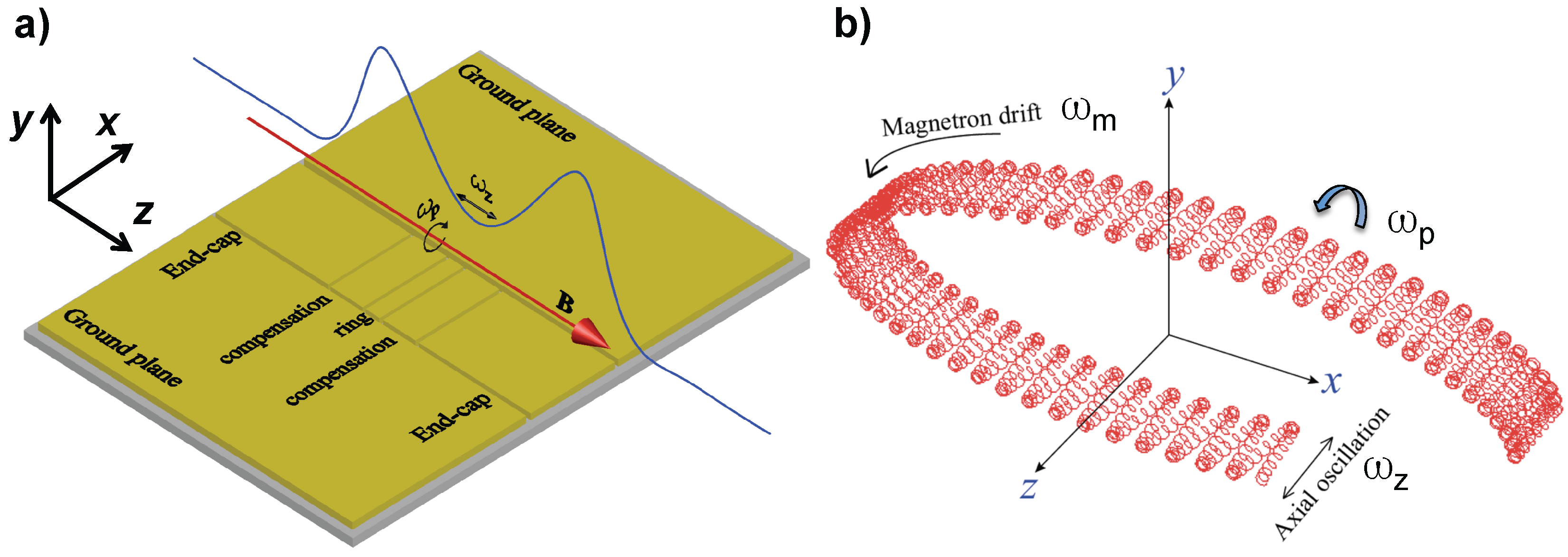
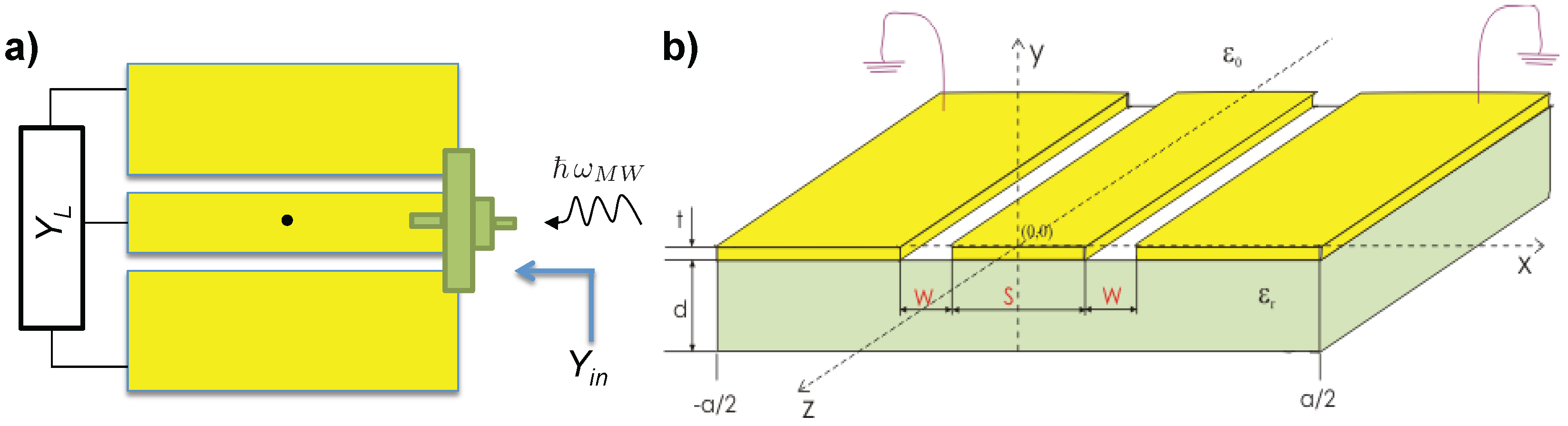
2. Basics of the Geonium Chip Planar Penning Trap

Figure 1a shows a sketch of the geonium chip. The ion trap is formed by five flat rectangular electrodes placed in the centre of of the chip and separated by very small (a few microns) insulating gaps [11]. The magnetic field source (not shown) is placed underneath the electrodes and is formed by a set of several planar, closed rectangular loops of superconducting currents [15,16]. The trap’s working principle is straightforward. The static magnetic field, B = B 0 · u ^ z , forces the electron (or in general ion) to follow a closed (cyclotron) orbit around u ^ z , hence trapping it “radially”, along the u ^ x and u ^ y axes. Static voltages applied to the electrodes generate a harmonic potential well, confining the particle “axially”, that is: along the u ^ z axis. The electron is captured at a height y 0 above the chip’s surface. The value of y 0 can be controlled by the ratio of the voltages applied to the end-caps V e to the voltage at the ring electrode V r . Typically y 0 can be varied within a few hundred micron up to a few mm [12].
The motion of the trapped electron is shown in Figure 1b. It is the superposition of three harmonic oscillators: the cyclotron and axial motions, with frequencies ω p and ω z , respectively, and the slow magnetron drift, with frequency ω m . These are given by [17]:
ω p = 1 2 ( ω c 2 ω z 2 ) + 1 2 ω c 2 ω 1 2 + ϵ 2 ω z 4 ; ω m = 1 2 ( ω c 2 ω z 2 ) 1 2 ω c 2 ω 1 2 + ϵ 2 ω z 4 .
ω z = 2 c 002 V r q m ; with ω c = q m B 0 ; ω 1 = ω c 2 2 ω z 2 .
In Equations (1) and (2) the symbols q , m represent the charge and mass of the trapped particle, respectively. The free cyclotron frequency is denoted by ω c , where B 0 is the strength of the magnetic field along u ^ z at y 0 . The symbols ϵ and c 002 represent the ellipticity and the curvature of the trapping potential, respectively [11]. In a magnetic field of B 0 = 1 T and with a ring voltage of V r = 1.0 V, the typical values of the motional frequencies of a trapped electron in the geonium chip are: ω p = 2 π · 28 GHz, ω z = 2 π · 30 MHz and ω m = 2 π · 30 kHz. The axial frequency ω z is determined by the value of the voltage applied to the trap electrodes alone and is fully independent of the strength of the magnetic field, ω z ω z ( B 0 ) .

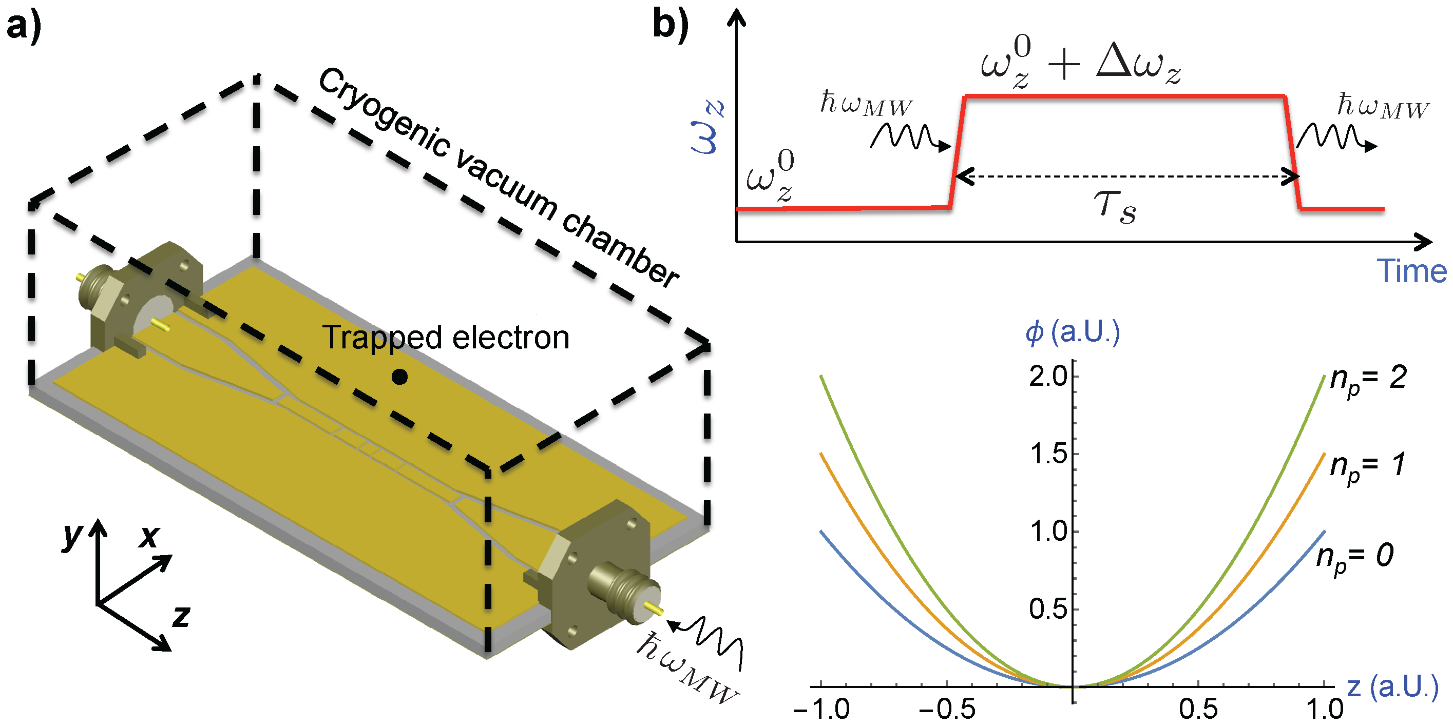
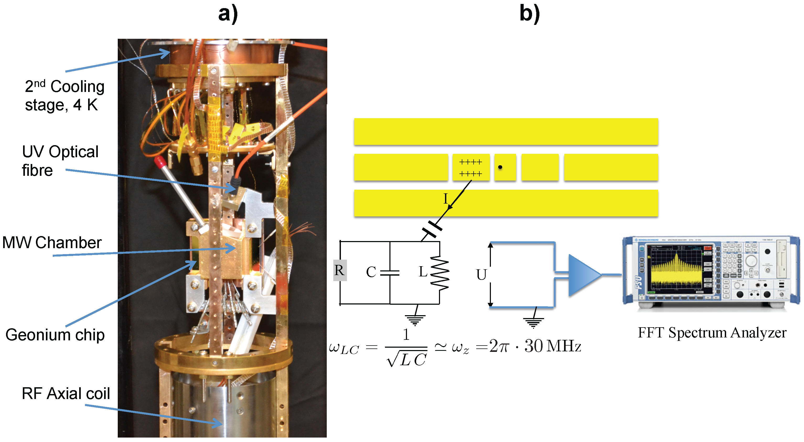
2.1. Overview of the Experimental Setup

Figure 2 shows an overview of the basic components which form the experimental setup. The cryostat consists of a pulse-tube cooler which brings the temperature down to around 4 K. As shown in the picture, the geonium chip is anchored to a copper structure which is in thermal equilibrium with the second cooling stage of the pulse-tube cooler. The trap can be loaded with electrons generated by the photoelectric effect with a pulse of UV light impacting onto the metallic surface of the chip. The UV light is guided towards the chip’s surface by a cryogenic optical fibre. The DC voltages generating the electrostatic potential are produced by high-precision voltage calibrators.
At 4 K the electron’s cyclotron oscillator is typically several quanta above the ground state [5]. In order to cool it further down to the ground state, the Sussex setup is planned to be enhanced with a miniature adiabatic demagnetisation refrigerator (ADR) developed at the Mullard Space Science Laboratory [18]. This device will bring the temperature down to around 80 mK, where the electron’s cyclotron oscillator effectively achieves the ground state [5]. This eliminates thermal MW noise and initialises the particle for the detection of signals made of single photons.

2.2. Detection of the Trapped Electron’s Axial Motion

The motion of the trapped particle can be detected through the current it induces upon the surface of the chip, as illustrated in Figure 2b. This detection technique was first proposed by Dehmelt [19] and has been profusely described in the literature (see for instance [20] and references therein). As explained in Section 3.3, the measurement of the axial motion critically determines the performance of the trapped electron as a single microwave photon detector.
As depicted in Figure 2b, the electron induces a positive charge density on the chip’s electrodes, which varies in time with the same periodicity as the trapped particle’s motion. The resulting induced AC-current I is forced to flow from the chip surface to ground along an LC circuit. The latter is tuned to resonate with ω z . Therefore, the induced current generates an AC-voltage U, which appears across the tuned resonator. The induced signal U is first amplified by a low-noise amplifier stage at 4 K [21,22]. The signal is then carried to the room temperature electronics, where it is further amplified and recorded in the frequency domain with a FFT spectrum analyser. Besides the cryogenic amplifier, the key element of the detection system is the LC resonator, typically a superconducting coil. Figure 2a shows the superconducting casing (Niobium) containing the resonator.
The main features of the electron’s axial motion detection, upon which the microwave photon detection relies, are listed below:
  • The detection is non destructive: the axial frequency can be monitored continuously, without losing the trapped particle [19].
  • The measurement of ω z occurs with the axial motion being in thermal equilibrium with the LC resonator, typically at 4 K or eventually even at higher temperatures [23].
  • The detection of the axial motion leaves the electron’s cyclotron quantum state unaffected [5]. Thus, while the axial motion is in thermal equilibrium with the LC resonator at 4 K, the cyclotron quantum state can be in thermal equilibrium with the 80 mK temperature provided by the ADR.
  • While ω z and the LC circuit must be resonantly coupled (see Figure 2b), the value of the trapping magnetic field, and therefore of ω p , can be freely chosen without affecting the detection of the axial motion.
  • The cyclotron and magnetron frequencies can be accurately obtained through the axial detection signal, by means of the mode-coupling technique [24]. This well established technique has been described in detail in [25].
  • The frequency ω z can be measured with an accuracy of 1 Hz in around 5 s. This is the lapse required to measure an FFT spectrum of 1 Hz resolution (∼1 s each) and average it for a good signal-to-noise ratio. As explained in Section 5, such long measurement time would not allow for high quantum efficiency in MW photon detection. However, frequency variations Δ ω z can be determined substantially faster, by recording the phase evolution of the axial motion but without waiting for a full 2 π oscillation [26]. This will permit very rapid MW photon detection, as detailed in Section 5.

3. Detection of Microwave Photons with a Trapped Electron

In general the cyclotron frequency has some dependence on the applied electrostatic voltages, however ω p is mainly determined by the strength of the magnetic field [27]. For fields above 0.1 T the electron’s motional frequency ω p can be approximated as the free cyclotron frequency ω c :
ω p ω c = q m B 0 ω p 2 π · [ 2.8 , 56 ] GHz , for B 0 [ 0.1 , 2 ] T .
As seen in Equation (3), the electron’s cyclotron frequency ω p falls within the microwave domain. This motional degree of freedom of the trapped particle can be used to detect microwave photons non destructively. In principle, the electron’s intrinsic magnetic dipole moment could also provide a measurable transition, potentially useful for the detection of microwave radiation [27]. However, the spin-microwave interaction is a magnetic dipole transition, thus several orders of magnitude weaker than the cyclotron-microwave interaction, which is an electric dipole transition. For this reason the former will no longer be considered here and we will focus on the interaction of microwave fields with the electron’s cyclotron motion.

3.1. Interaction of a Cyclotron Quantum Harmonic Oscillator with an Itinerant Microwave

Figure 3a presents a sketch of the basic MW photon detection scheme. The radiation is guided towards the trapped electron following a Coplanar-Waveguide transmission-line on the chip. The figure illustrates the photon travelling along a Coplanar-Waveguide (CPW) coincident with the transmission-line formed by the trap’s electrodes. Although this might be a possibility, it is not a requirement: a different CPW or another kind of transmission-line can be used to guide the microwave radiation to the electron. For simplicity, here we assume this topology, however, the results obtained can be generalised to other waveguides or transmission-lines.
One essential feature of the setup in Figure 3a is the sketched cryogenic vacuum chamber, which encloses the trapping volume. The chamber acts also as a rectangular microwave cavity. We assume that the frequency of the photons to be detected ω M W does not match any of the possible modes sustained by this cavity [28]. Thus, the microwave radiation within the trapping region can exist only as a propagation mode of the CPW. Moreover, the spontaneous emission of energy from the cyclotron oscillator into free space (i.e., into the cavity volume) will be strongly inhibited too. This has been observed experimentally with an electron trapped inside a detuned cylindric cavity [5], achieving lifetimes of the order of tens of seconds [29]. However, in our case the spontaneous emission of cyclotron radiation into any of the propagation modes of the CPW transmission-line is not inhibited, since this is used for the MW detection. The details are discussed in Section 5.1.

3.2. Dynamics of Two Coupled Quantum Harmonic Oscillators

Both the cyclotron motion and the radiation field are quantum harmonic oscillators. The basic Hamiltonian of the cyclotron-MW interaction is thus [30]:
H = ω p a p a p + 1 2 + ω M W a M W a M W + 1 2 + Ω a M W a p + a M W a p .
In Equation (4) a p , a p represent the creation and annihilation operators of the cyclotron degree of freedom, respectively. Similarly, a M W , a M W denote the creation and annihilation operators of the propagating microwave mode, respectively. The symbol is the reduced Planck’s constant and Ω represents the coupling strength (with the dimensions of a frequency). The dynamics of the Hamiltonian in Equation (4) has been solved in [30], where incoherent losses of the microwave radiation and spontaneous emission are ignored. The electron’s cyclotron degree of freedom is a multi-level system and the dynamics in Equation (4) can be very complex when including interactions with waves carrying more than one quantum of energy. In contrast to most other quantum microwave sensors proposed and/or being developed, based upon “lambda” three-level systems, (see [4] and references therein) the electron’s cyclotron quantum harmonic oscillator can detect several microwave photons simultaneously [5]. While that can be very advantageous in many situations, here we restrict the discussion to the simplest case where the radiation contains only one photon per detection event.

3.3. Principle of Microwave Photon Detection: The Continuous Stern-Gerlach Effect

When hit by one MW photon of frequency close to ω p , the trapped electron’s cyclotron oscillator increases its energy in one quantum. This fundamental process can be measured accurately [5]. The cyclotron quantum jumps are observed by means of the so-called continuous Stern-Gerlach effect [31]. This is illustrated in the upper diagram of Figure 3b. Once a photon is absorbed by the cyclotron motion, the unperturbed axial frequency ω z 0 changes slightly by Δ ω z , such that the resulting axial frequency is ω z = ω z 0 + Δ ω z . Here ω z 0 denotes the axial frequency when the cyclotron oscillator is in the quantum ground state, n p = 0 . The continuous Stern-Gerlach effect relies upon the introduction of some curvature in the magnetic field, B 2 0 , a configuration known as a “magnetic bottle” [27]. This curvature causes the effective axial potential experienced by the electron to depend upon the quantum state of the cyclotron motion n p [31], as sketched in Figure 3b. The cyclotron quantum jump caused by the absorption of one photon is observable through Δ ω z . This amounts to [31]:
Δ ω z = q B 2 m 2 ω z 0 .
In general, when the electron absorbs Δ n p { 0 , 1 , 2 , 3 , } microwave quanta, the variation of the axial frequency is Δ ω z ( Δ n p ) = Δ ω z · Δ n p , and is directly proportional to the number of photons detected. Therefore, the detection of the microwave radiation is provided by the measurement of the axial frequency, described in Section 2.2. Hence, that measurement determines the ability of the trapped electron as a microwave photon transducer.

3.4. Generation of a Magnetic Bottle in the Geonium Chip

A typical magnetic field curvature of B 2 = 1.5 mT/mm 2 as used in [5], and with ω z 0 = 2 π · 30 MHz, will result in Δ ω z = 2 π · 30 Hz for a cyclotron quantum jump, Δ n p = 1 . This Δ ω z delivers the observable signal of one MW photon and it can be measured unambiguously [5]. Moreover, B 2 broadens the particle’s cyclotron resonance to Δ ω p / ω p 10 7 [32], thus, in principle, making photons with frequencies ω p ± Δ ω p detectable. For ω p = 2 π · 28 GHz, Δ ω p = 2 π · 2.8 kHz. This is a sharp and highly filtered detection window. As discussed in Equation (3), by varying B 0 , the cyclotron frequency ω p can be varied, making the electron become resonant -and therefore sensitive- to MW in a very broad range of frequencies. Photons at around 150 GHz have been detected in the cylindric trap used in [5].
Conventional Penning trap quantum-jump spectrometers usually employ one of the trap’s electrodes to implement the required magnetic bottle [27]. Typically the ring electrode is made of a ferromagnetic material, such as nickel, iron, cobalt, samarium or alloys of these [32]. The ferromagnetic electrode locally distorts the magnetic field created by the superconducting solenoid, providing the non-vanishing B 2 term of Equation (5). In our case, the magnetic curvature is created by adjusting the chip’s superconducting currents [15,16], such that B 2 0 . Numerical examples can be found in the given references. In general, due to the close proximity of the electron in the geonium chip to the magnetic field source, magnetic bottles substantially stronger than B 2 = 1.5 mT/mm 2 of [5] might be achieved. A high curvature B 2 provides a big cyclotron quantum jump Δ ω z , making it easier and faster to detect. This will be critical for MW detection, as discussed in Section 5.2.

3.5. Quantum Non Demolition Photon Detection

The continuous Stern-Gerlach effect allows for observing the variation of the electron’s cyclotron quantum state by monitoring another degree of freedom of the electron, namely its axial frequency ω z . When a cyclotron quantum jump is observed through Δ ω z of Equation (5), the actual detection process, i.e., the measurement of the axial frequency, does not destroy irreversibly the cyclotron energy: this remains stored in the electron [5]. This is a quantum non demolition detection (QND) and, in principle, the microwave photon can be recovered and further used within a microwave quantum circuit. The microwave quantum will be available only for a time span equal to the radiative lifetime of the cyclotron state, τ s , as shown in Figure 3b.

4. Quantum Efficiency of MW Photon Detection by a Single Trapped Electron

We now calculate the quantum efficiency of microwave photon detection by a single electron transducer in a geonium chip. As mentioned in Section 3.2 we restrict the discussion to the simplest case where only one photon is present per detection event. Furthermore, we also assume that the MW photon and the electron are perfectly, or very nearly, resonant ω M W ω p . The discussion is semi-classical, where we first estimate the amplitude of the electric field of a classical EM-wave carrying the energy of one photon. We then compute the absorption probability by the quantised cyclotron oscillator. Moreover, we ignore photon losses due to the MW propagation along the CPW of Figure 3a. These will be relevant for the implementation of an efficient geonium chip MW detector, however their minimisation is an engineering problem beyond the scope of this article.

4.1. Electric Field Strength of a Single Itinerant Photon Propagating along a CPW Transmission-Line

The power transported by a microwave travelling along the CPW transmission-line (Figure 3a) is given by P M W = 1 2 V I * , where V and I represent the voltage and current associated with the propagating wave, respectively. Denoting by Y i n the input admittance of the electron + loaded CPW-line “seen” by the incoming photon (see Figure 4a), the power can be written as P M W = 1 2 | V | 2 Y i n [28]. This power is provided by the energy of a photon, ω M W , multiplied by the rate at which photons enter the geonium chip: 1 / τ M W . As discussed before, we assume that the period τ M W is sufficiently long for having only one photon per detection event. Thus, the voltage associated with this train of microwave photons is:
P M W = 1 2 | V γ | 2 Y i n = ω M W τ M W V γ = 2 ω M W τ M W Y i n .
The voltage V γ gives the potential difference between the central conducting strip and the ground-planes in the CPW produced by a wave composed of one photon arriving every τ M W seconds. In general, CPW transmission-lines support two possible quasi-TEM propagation modes: the even and the odd modes [33]. The electric field component of these two modes has been calculated in [34]. For a voltage of 1 V, their expressions at the position of the trapped electron, y 0 , are:
E C P W odd = 4 π W n = 1 sin n π W a sin n π W + S a n 2 + a 2 λ M W 2 a 2 ν M W 2 c 2 exp 2 π y 0 a n 2 + a 2 λ M W 2 a 2 ν M W 2 c 2 .
E C P W even = 4 π W n = 0 sin 2 n + 1 2 π W a cos 2 n + 1 2 π W + S a 2 n + 1 2 exp 2 π y 0 a 2 n + 1 2 2 + a 2 λ M W 2 a 2 ν M W 2 c 2 .
In Equations (7) and (8) c is the speed of light in vacuum. The transverse dimensions of the CPW are defined in Figure 4b. S is the width of the central conducting strip, W is the gap between the latter and the “ground-planes” and a is the total chip’s width. The wavelength λ M W , corresponding to the photon’s frequency ( ν M W = ω M W / 2 π ), depends on the trap’s substrate electric permittivity ϵ r , its thickness d, the thickness of the conducting layer t and the dimensions S , W [35]. Both electric fields in Equations (7) and (8) have a strong dependence on the position y 0 . Moreover E C P W even is oriented along the u ^ x axes, while E C P W odd points along u ^ y , in the coordinate system of Figure 1, Figure 3 and Figure 4 [34]. The electric field of the 1-photon wave introduced in Equation (6) is obtained by multiplying ( E C P W even , E C P W odd ) times the voltage V γ .

4.2. Probability of MW Photon Absorption by the Quantum Cyclotron Oscillator

The probability that the microwave signal propagating along the CPW-line induces a transition in the electron’s cyclotron quantum state n p = 0 n p = 1 is proportional to the matrix element | 0 | ( E · P ) | 1 | 2 , where E = V γ ( E C P W even , E C P W odd , 0 ) and P = q ( X , Y , Z ) is the electric dipole moment operator of the trapped quantum cyclotron oscillator. The absorption probability rate can be computed using Fermi’s golden rule [36]:
Γ | 0 | 1 = 2 π | 0 | E · p | 1 | 2 g p ( E ) = 2 π q 2 V γ 2 | 0 | ( E C P W even X + E C P W odd Y ) | 1 | 2 g p ( E ) .
In Equation (9), the function g p ( E ) = 1 2 π 1 ω p is the density of final available energy states for the cyclotron motion. The factor 1 / ( 2 π ) is a normalisation constant which accounts for all possible values of the phase impinged by the photon on the cyclotron harmonic oscillator, which is one single degree of freedom but it evolves in the xy plane. Furthermore, the CPW is usually wired such that only one mode but not the other can propagate. Thus, we separate the contribution of each of them, getting the even and odd absorption probability rates:
Γ | 0 | 1 even = 1 2 ω p q 2 V γ 2 | E C P W even | 2 | 0 | X | 1 | 2 ; Γ | 0 | 1 odd = 1 2 ω p q 2 V γ 2 | E C P W odd | 2 | 0 | Y | 1 | 2 .
The matrix elements | 0 | X | 1 | 2 and | 0 | Y | 1 | 2 can be computed using the creation and annihilation operators, a p , a p , defined in Equation (4). The result is | 0 | X | 1 | 2 = | 0 | Y | 1 | 2 = 2 m ω 1 2 m ω p [37]. Now, substituting V γ of Equation (6) and taking into account that ω p ω M W , we get:
Γ | 0 | 1 even = q 2 m ω p Y i n | E C P W even | 2 1 τ M W ; Γ | 0 | 1 odd = q 2 m ω p Y i n | E C P W odd | 2 1 τ M W .
From Equation (11) we can compute the “internal” quantum efficiency, η internal , defined as the photon absorption probability rate divided by the number of incident photons per unit time ( = 1 / τ M W ):
η internal even ( y 0 ) = 1 ω p q 2 | E C P W even | 2 m 1 Y i n ; η internal odd ( y 0 ) = 1 ω p q 2 | E C P W odd | 2 m 1 Y i n .
In Equation (12) we have made explicit the dependence of the internal quantum efficiency upon the trapping height, caused by the strong variation of | E C P W ( odd , even ) | 2 (and also of Y i n ) with y 0 .

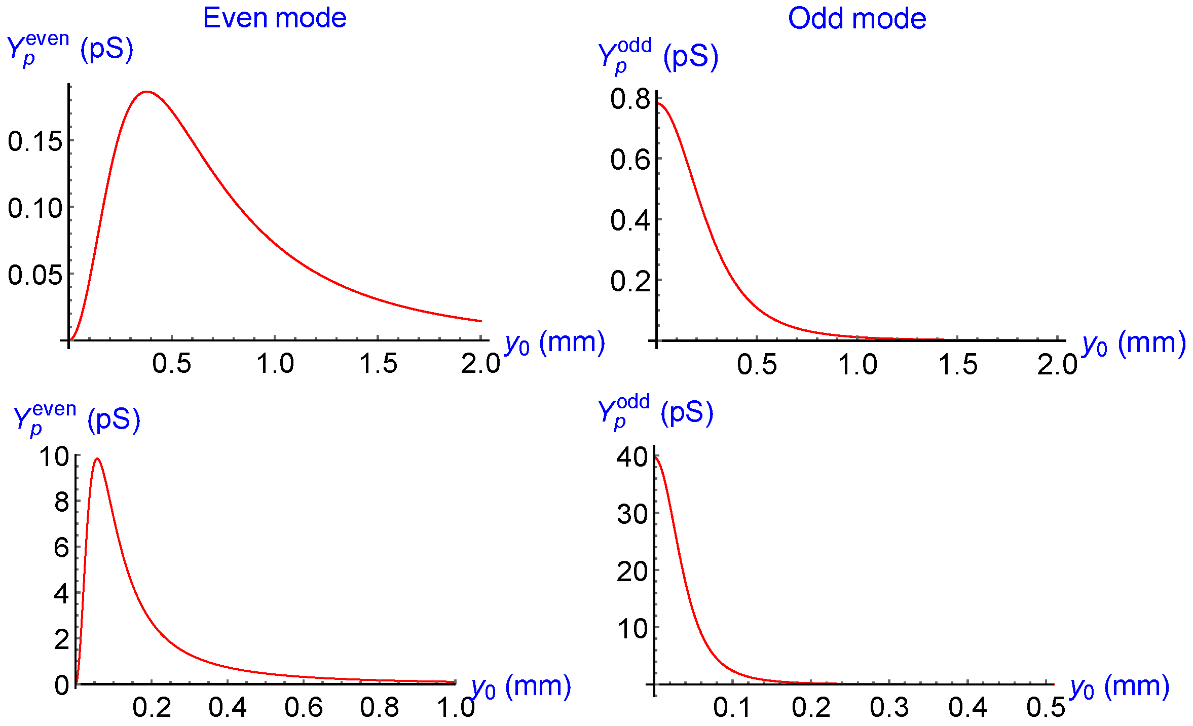
Characteristic Admittance of the Trapped Electron

Dehmelt demonstrated that each motional degree of freedom of a trapped ion behaves as an electric LC-circuit [19], with equivalent inductance L i o n and capacitance C i o n , such that ω i o n = 1 / C i o n L i o n . For the electron’s cyclotron motion, the equivalent inductance is given by [20]: L p even = m q 2 | E C P W even | 2 and L p odd = m q 2 | E C P W odd | 2 . Thus, the equivalent inductance (and capacitance) is not an intrinsic property of the particle, but depends on its electric coupling to the trap or transmission-line (through the induced charges, as in Figure 2). Moreover, a simple calculation shows that 1 / ( ω p L p ( even , odd ) ) = C p ( even , odd ) / L p ( even , odd ) , which has the dimensions of an admittance, similar to the characteristic admittance of a transmission-line [28]. Thus, for each of the propagations modes of the CPW, we define the characteristic admittance of the trapped cyclotron oscillator as:
Y p even = 1 ω p L p even = C p even L p even ; Y p odd = 1 ω p L p odd = C p odd L p odd .
Hence, the electron + CPW equivalent circuit behaves as two admittances coupled in parallel. The overall input admittance “seen” by the incoming microwave photon Y i n (Figure 4a) is therefore:
Y i n even = Y L C P W + Y p even ; Y i n odd = Y L C P W + Y p odd .
In Equation (14), Y L C P W is the transformed value of the load admittance, Y L , taken at the electron’s location along the CPW path. Y L C P W will depend on the the load, Y L , the CPW’s characteristic admittance, Y 0 C P W , and the electrical distance to the electron’s position in the circuit from Y L [28].

4.3. Internal Quantum Efficiency of Microwave Photon Detection

Using Equations (12)–(14), we can finally write the internal quantum efficiencies as:
η internal even ( y 0 ) = Y p even ( y 0 ) Y L C P W + Y p even ( y 0 ) ; η internal odd ( y 0 ) = Y p odd ( y 0 ) Y L C P W + Y p odd ( y 0 ) .
Since all admittances are real positive numbers, Equation (15) shows that, for both CPW modes, η internal ( y 0 ) 1 , as is expected for a well defined quantum efficiency function. It also shows that the electron and the CPW operate as a “current divider” (= “beam-splitter” ), where the photon either continues propagating along the transmission-line towards the load or it is absorbed by the quantum cyclotron. The reflection coefficient at the input port of the geonium chip (see Figure 3a) can be easily computed with the input admittance of Equation (14) [28]. This allows for a reflection-free design (admittance matching) of the transmission-line that guides the MW signal towards the chip (not shown in Figure 3). Notice, however, that a perfect admittance matching only avoids reflections at the chip input, but it does not guarantee perfect detection efficiency, η internal = 1 .
From Equation (15), for both modes we have: η internal 1 Y p ( y 0 ) Y L C P W . The electron’s cyclotron admittance Y p ( y 0 ) will increase when its capacitance grows, C p , i.e., when the particle’s ability to store electric energy becomes larger. This implies necessarily that the electric field of the CPW at the electron’s position, | E C P W ( y 0 ) | , must be maximised.
An example of the electron cyclotron characteristic admittance for the two CPW modes has been computed in Figure 5. The example shows that Y p is, in general, a very small number, of the order of a few pS. Thus, a significant internal quantum efficiency can only be achieved if the admittance of the load at the electron’s position vanishes: Y L C P W 0 . That is, the load Y L must become an open-circuit at the location of the quantum cyclotron oscillator. In this case the MW current has no other option but to “propagate” along the electron. It remains to be seen how ideal the open-circuit can be created, since any imperfections or leaks leading to Y L C P W > 0 will reduce substantially the quantum efficiency of photon detection, eventually making it vanish. In a superconducting chip, those leaks will be caused by the dielectric losses of the substrate. These are very low for materials such as sapphire, with a loss tangent of ∼ 4 × 10 8 at 4 K [38]. With this, an estimation of Y L C P W can be obtained by modelling it as a short-circuit terminated single-stub (see for instance [28]) with a length of ∼1–2 mm from the electron’s position. A value of Y L C P W 900 pS (at 4 K) can be estimated with that simple model when a characteristic admittance of 20 mS of the single stub is assumed. Such estimation would anticipate modest internal quantum efficiencies around 1%–2% for the particular example of Figure 5 (bottom graphs). However, further optimisation of the transmission-line geometry, the single-stub and a potential further reduction of dielectric losses at 80 mK (i.e., well below the 4 K used in [38]), might significantly increase these values. In Section 6 further improvements in the internal quantum efficiency will be introduced, by scaling up from one to several trapped electrons as MW absorbers.

5. Speed of Quantum Jump Detection versus Cyclotron Radiative Lifetime

The efficiencies η internal even and η internal odd derived in Equation (15) provide only the probability that an incident photon will cause a cyclotron quantum jump in the trapped electron. For this transition to be detected—and therefore the photon to be “counted—the measurement of Δ ω z (see Figure 3a) must occur faster than the radiative lifetime, τ s , of the electron’s excited state | 1 . Otherwise, the absorption event will go unnoticed. If we denote by τ m the time required to measure Δ ω z , then the overall quantum efficiency of the geonium chip MW photon detector can be written as:
η overall even = η internal even θ ( τ s τ m ) ; η overall odd = η internal odd θ ( τ s τ m ) .
In Equation (16) θ ( τ s τ m ) represents the Heaviside theta function. Hence, incident photons might induce cyclotron quantum jumps, however, these will only be detected if the resulting change of the electron’s axial frequency is measured rapidly enough: τ m < τ s . In order to evaluate Equation (16) we first need to compute the radiative lifetime τ s and then the measurement time τ m .

5.1. Quantum Cyclotron Radiative Lifetime in a CPW Transmission-Line

As explained in Section 3.1 and Section 3.5, the cyclotron spontaneous emission in the trapping volume is negligible, hence we need to determine the spontaneous decay rate of the quantum cyclotron oscillator into any of the propagating modes of the CPW transmission-line. The calculation is very similar to the one performed in Section 4.2. Using again Fermi’s golden rule [36], we have:
1 τ s = 2 π 2 | 0 | E v a c · p | 1 | 2 g C P W ( ω p ) .
In Equation (17), E v a c represents the electric field of the vacuum in the coplanar-waveguide and g C P W ( ω p ) the density of available propagation modes in that transmission-line, at the frequency ω p . While in the absorption event we had a propagating microwave, now the situation is different. There is no travelling photon and the vacuum field must be found in another way as in Section 4.1. Thus, in order to compute E v a c and g C P W ( ω p ) we model the CPW as an uni-dimensional microwave cavity of (very long) length L . In this cavity, the energy stored is given by [28]: L × 1 2 C V 0 2 , where C here represents the capacitance per unit length of the CPW and V 0 is the voltage. Equating the stored energy to the zero-point energy of the EM field at ω p , we obtain the voltage V v a c corresponding to the vacuum field in the CPW:
L × 1 2 C V v a c 2 = 1 2 ω p V v a c = ω p L C E v a c = V v a c ( E C P W even , E C P W odd , 0 ) .
An analytic expression for C can be found in [35]. The density of states within the uni-dimensional CPW transmission-line can be easily computed to: g C P W ( ω ) = 2 L c . The factor 2 comes from the availability of two possible senses of propagation of the MW. With this and Equation (18), we obtain the radiative lifetimes:
τ s even ( y 0 ) = m c C 2 π q 2 1 | E C P W even | 2 = c C L p even 2 π ; τ s odd ( y 0 ) = m c C 2 π q 2 1 | E C P W odd | 2 = c C L p odd 2 π .
In Equation (19) we have assumed, as in Section 4.2, that the CPW is wired such that only one mode -the even or the odd- is accessible, while the other is totally suppressed and hence inhibited. If that is not the case, then the overall radiative lifetime is 1 τ s overall = 1 τ s even + 1 τ s odd . Furthermore, as expected from general quantum optics theory, each τ s in Equation (19) is proportional to the corresponding electron’s inductance, opposing the inverse dependence of the particle’s characteristic admittance with L p (see Equation (13)). Therefore, the design of the transmission-line feeding in the microwave photons will necessarily demand a compromise between τ s and Y p . However, the internal quantum efficiency can be maximised through Y L C P W as well, without influencing the radiative lifetime. Hence, two degrees of freedom are available which might be independently optimised for providing both, high internal quantum efficiency, η internal , and sufficient radiative lifetime, τ s τ m .
Figure 6 shows an example calculated with the expressions obtained in Equation (19), using the same dimensions for the CPW as in Figure 5. For values y 0 > 1 mm the cyclotron lifetime becomes of the order of a few to hundred seconds. For y 0 1 mm τ s falls within the range of a few hundred ms for both CPW modes. Only at very low trapping heights does the lifetime start diverging again for the even mode, due to the vanishing | E C P W even | for y 0 0 [20]. The regions of lowest τ s coincide with those of maximal internal quantum efficiency, as plotted in Figure 5. Hence, for this example, the measurement time τ m required for observing the cyclotron quantum jump should become lower than the obtained several hundred ms.

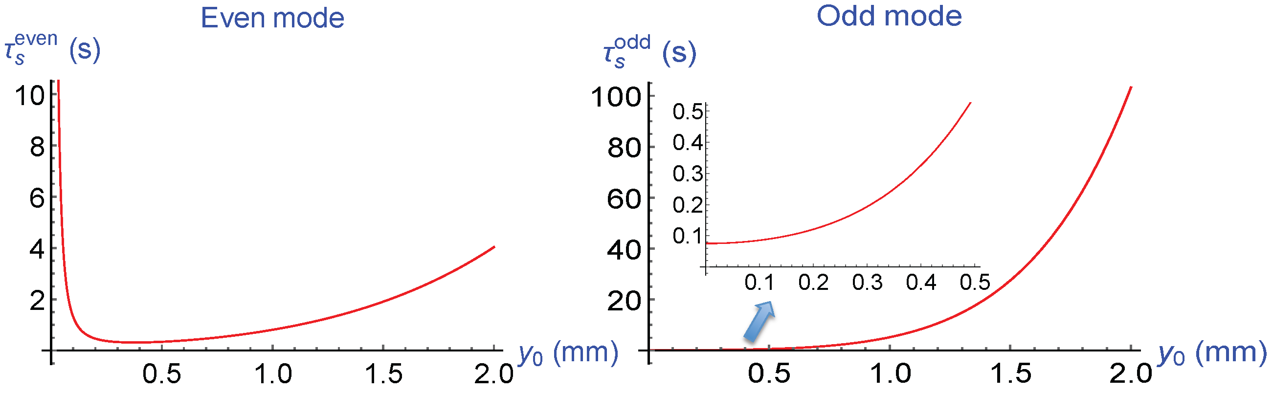
5.2. Measurement Time of Δ ω z

As discussed in Section 2.2 the measurement of ω z is very slow for achieving high quantum efficiency. Still, the detection of the cyclotron quantum jumps requires only the determination of the frequency shift Δ ω z . The measurement of the ion’s motional phase, first developed in [26], allows for resolving Δ ω z rapidly, much faster than the full measurement of ω z . That technique uses the same detection scheme as described in Section 2.2, however, instead of measuring the amplitude of the induced voltage (Figure 2b), it measures its phase, which is directly linked to the phase of the particle’s axial oscillation. As explained in [26], the measurement time is given by the following simple expression:
τ m = σ ( Δ ϕ ) Δ ω z
In Equation (20) σ ( Δ ϕ ) represents the minimum axial phase-difference required to distinguish between the particle at n p = 0 (i.e., with ω z = ω z 0 ) from the state n p = 1 (i.e., with ω z = ω z 0 + Δ ω z ) [26]. The value of σ ( Δ ϕ ) is an empirical quantity governed by the specifics of the experimental setup, particularly by the stability of the electrostatic voltages. Given σ ( Δ ϕ ) , from Equation (20) it is clear that the stronger the magnetic bottle the smaller the measurement time τ m will be. In the early experiments of [26] quantum jumps of 100 mHz were determined in 800 ms, with σ ( Δ ϕ ) = 45 . Thus, a quantum jump of 10 Hz would require τ m = 8 ms. In the geonium chip, due to the proximity of the electron to the magnetic source, magnetic bottles might be created with Δ ω z well above 10 Hz, eventually achieving a 1 kHz or more, thus further reducing the measurement time to τ m = 80 μ s or less, hence well below the values of τ s obtained in Section 5.1.

6. Comparison with Other Single Microwave Photon Detectors

In this section we present a basic comparison between the trapped electron and other possible single MW photon detectors. We limit the discussion to artificial atoms made with superconductors in a chip as described in [2,3].
For the absorption of one photon, the electric dipole moment (EDM) associated to that quantum transition in the cyclotron oscillator is given by d cyclotron = q | 0 | X | 1 | = q | 0 | Y | 1 | = q 2 / ( 2 m ω p ) , as derived in Section 4.2. The value of this matrix element can be compared to the equivalent transition dipole moment of any other quantum system proposed for single MW photon detection. In particular, a Cooper Pair Box (CPB) has a typical transition EDM of d CPB = 20,000 atomic units (≃36,000 D) [39,40]. Hence, at the operation frequency in those circuit-QED experiments of ∼7 GHz, the ratio between both EDMs is d CPB d cyclotron 30 . This implies that the interaction of a photon with a CPB is about 30 times stronger than with a trapped electron. Since a microwave cavity with a quality factor of Q = 10 4 suffices for the CPB to achieve the strong-coupling regime in circuit-QED [39], a cavity of Q 3 × 10 5 would also allow for a trapped electron to interact coherently with the MW radiation. The comparison of the quantum efficiencies of MW photon detection of the artificial atom and electron is, however, not as straightforward as comparing the dipole moments. In contrast to the quantum cyclotron, the devices investigated in [2,3] are not QND sensors, hence the MW energy is irreversibly lost after the detection event. Moreover, they operate as a “lambda” three-level system, which implies that they can achieve a maximum of only η = 0.5 [2] (with only one MW absorber). The electron is not subject to this limitation predicted for any other systems with that level structure [2]. The cyclotron quantum state is monitored through another degree of freedom (the axial motion), hence a “lambda” three-level structure is unnecessary for the electron to operate as a MW transducer. This essential difference overcomes the limitation of the systems discussed in [2,3] and would allow, in principle, for 100 % quantum efficiency. Furthermore, a solution proposed for superconducting artificial atoms to break the η = 0.5 barrier is the use of several MW absorbers in a chip [2,3]. In our case, loading N electrons in the trap would increase the collective characteristic admittance to N · Y p . Moreover, in the “superradiant” absorption regime -where all N trapped electrons interact simultaneously with the incoming MW radiation- absorbing one photon implies a “collective” cyclotron quantum jump of Δ n p = N · 1 . Thus, the collective signal Δ ω z × Δ n p (Equation (5)) remains unchanged with respect to the single electron case, and so does the photon detection time τ m of Equation (20). Although the radiation time τ s would be reduced by a factor N (see Section 5.2), this would still be above τ m for N 1000 . In summary, while one single electron could theoretically suffice, the use of N trapped electrons might make the geonium chip a more efficient MW photon detector technology, helping increase the detector’s admittance discussed in Section 4.3. The potential use of N trapped electrons will be further investigated in detail in future publications.

7. Conclusions

In this article we have studied the basic features of an electron trapped in a geonium chip as a detector of single microwave photons. We have shown that the trapped electron is a QND, tuneable microwave sensor, whose frequency band is very broad, potentially up to well above 100 GHz. The detection frequency can be adjusted by varying the trapping magnetic field of the geonium chip. While the electron is potentially capable of detecting several quanta of MW radiation simultaneously, we have limited the discussion to the case of single photon events. We have calculated the internal quantum efficiency and the quantum cyclotron radiative lifetime. Both these quantities determine the overall quantum efficiency for microwave photon detection with a trapped particle. The calculations have been performed assuming that the interaction between the electron and the photon is mediated by a CPW transmission-line. However, the formulas obtained for the internal quantum efficiency and the cyclotron radiative lifetime have general validity. They can be used with other types of transmission-lines or waveguides, such as microstrips, strip-lines, slot-lines, dielectric waveguides, etc. We have derived the characteristic admittance of the quantum cyclotron oscillator, which critically determines the internal quantum efficiency. Furthermore, we have identified the main technical challenges in the fabrication of the future generation geonium chip for reaching high quantum efficiency microwave photon detection. These are the implementation of a -close to ideal- open-circuit at the location of the electron along the coupling transmission-line, and the reduction of the time necessary to track a cyclotron quantum jump, requiring the creation of a strong magnetic bottle. At Sussex we are currently developing this device and we have provided an overview of the experimental setup.

Acknowledgments

J.V. acknowledges strong support from EPSRC, through the Quantum Technology Fellowship EP/N003675/1. The work is also supported by the University of Sussex through the RDF award, HEIF funds and by the Sussex Innovation Centre.

Author Contributions

J.V. conceived the main idea; A.C., J.H.L. and J.P. have designed and built the experimental setup and contributed to the further conceptual development of the geonium chip quantum technology; J.V. wrote the paper.

Conflicts of Interest

The authors declare no conflict of interest.

Abbreviations

The following abbreviations are used in this manuscript:
MDPIMultidisciplinary Digital Publishing Institute
ADRAdiabatic Demagnetisation Refrigerator
QNDQuantum Non Demolition
MWMicrowave
EMElectromagnetic
CPWCoplanar-Waveguide
FFTFast Fourier Transform
EDMElectric Dipole Moment
CPBCooper Pair Box

References

  1. Manninen, A.J.; Kemppinen, A.; Lehtinen, J.; Mykkänen, E.; Amato, G.; Enrico, E.; Lacquaniti, V.; Kataoka, M.; Lindström, T.; Dolata, R.; et al. Towards measurement and control of single-photon microwave radiation on chip. In Proceedings of the 2015 1st URSI Atlantic Radio Science Conference (URSI AT-RASC), Gran Canaria, Spain, 16–24 May 2015; p. 1.
  2. Romero, G.; García-Ripoll, J.J.; Solano, E. Microwave Photon Detector in Circuit QED. Phys. Rev. Lett. 2009, 102, 173602. [Google Scholar] [CrossRef] [PubMed]
  3. Peropadre, B.; Romero, G.; Johansson, G.; Wilson, C.M.; Solano, E.; García-Ripoll, J.J. Approaching perfect microwave photodetection in circuit QED. Phys. Rev. A 2011, 84, 063834. [Google Scholar] [CrossRef]
  4. Sathyamoorthy, S.R.; Stace, T.M.; Johansson, G. Detecting itinerant single microwave photons. Comptes Rendus Physique 2016, 17, 756–765. [Google Scholar] [CrossRef]
  5. Peil, S.; Gabrielse, G. Observing the Quantum Limit of an Electron Cyclotron: QND Measurements of Quantum Jumps between Fock States. Phys. Rev. Lett. 1999, 83, 1287–1290. [Google Scholar] [CrossRef]
  6. Ciaramicoli, G.; Marzoli, I.; Tombesi, P. Scalable quantum processor with trapped electrons. Phys. Rev. Lett. 2003, 91, 017901. [Google Scholar] [CrossRef] [PubMed]
  7. Ciaramicoli, G.; Marzoli, I.; Tombesi, P. Trapped electrons in vacuum for a scalable quantum processor. Phys. Rev. A 2004, 70, 032301. [Google Scholar] [CrossRef]
  8. Lamata, L.; Porras, D.; Cirac, J.I.; Goldman, J.; Gabrielse, G. Towards electron-electron entanglement in Penning traps. Phys. Rev. A 2010, 81, 022301. [Google Scholar] [CrossRef]
  9. Ciaramicoli, G.; Marzoli, I.; Tombesi, P. Quantum spin models with electrons in Penning traps. Phys. Rev. A 2008, 78, 012338. [Google Scholar] [CrossRef]
  10. Dehmelt, H.G. Experiments with an isolated subatomic particle at rest. Rev. Mod. Phys. 1990, 62, 525. [Google Scholar] [CrossRef]
  11. Verdú, J. Theory of the coplanar waveguide Penning trap. New J. Phys. 2011, 13, 113029. [Google Scholar] [CrossRef]
  12. Pinder, J.; Verdú, J. A planar Penning trap with tunable dimensionality of the trapping potential. Int. J. Mass Spectrom. 2013, 356, 49–59. [Google Scholar] [CrossRef]
  13. Thompson, R.C.; Donnellan, S.; Crick, D.R.; Segal, D.M. Applications of laser cooled ions in a Penning trap. J. Phys. B At. Mol. Opt. Phys. 2009, 42, 154003. [Google Scholar] [CrossRef]
  14. Xian, F.; Hendrickson, C.; Marshall, A. High resolution mass spectrometry. Anal. Chem. 2012, 84, 708–719. [Google Scholar] [CrossRef] [PubMed]
  15. Verdú, J. Ion Trap. U.S. Patent US 8,362,423 B1, 29 January 2013. [Google Scholar]
  16. Verdú, J. Ion Trap. WO Patent WO 2,013,041,615 A3, 10 May 2013. [Google Scholar]
  17. Kretzschmar, M. Theory of the elliptical Penning trap. Int. J. Mass Spectrom. 2008, 275, 21–33. [Google Scholar] [CrossRef]
  18. Bartlett, J.; Hardy, G.; Hepburn, I. Performance of a fast response miniature Adiabatic Demagnetisation Refrigerator using a single crystal tungsten magnetoresistive heat switch. Cryogenics 2015, 72, 111–121. [Google Scholar] [CrossRef]
  19. Dehmelt, H.G.; Walls, F.L. Bolometric technique for the rf spectroscopy of stored ions. Phys. Rev. Lett. 1968, 21, 127–131. [Google Scholar] [CrossRef]
  20. Al-Rjoub, A.; Verdú, J. Electronic detection of a single particle in a coplanar-waveguide Penning trap. Appl. Phys. B 2012, 107, 955–964. [Google Scholar] [CrossRef]
  21. Jefferts, S.R.; Heavner, T.; Hayes, P.; Dunn, G.H. Superconducting resonator and a cryogenic GaAs field-effect transistor amplifier as a single-ion detection system. Rev. Sci. Instrum. 1993, 64, 737–740. [Google Scholar] [CrossRef]
  22. Ulmer, S.; Blaum, K.; Kracke, H.; Mooser, A.; Quint, W.; Rodegheri, C.; Walz, J. A cryogenic detection system at 28.9 MHz for the non-destructive observation of a single proton at low particle energy. Nucl. Instrum. Methods Phys. Res. Sect. A 2013, 705, 55–60. [Google Scholar] [CrossRef]
  23. Djekic, S.; Alonso, J.; Kluge, H.J.; Quint, W.; Stahl, S.; Valenzuela, T.; Verdú, J.; Vogel, M.; Werth, G. Temperature measurement of a single ion in a Penning trap. Eur. Phys. J. D 2004, 31, 451–457. [Google Scholar] [CrossRef]
  24. Verdú, J.; Alonso, J.; Djekic, S.; Kluge, H.J.; Quint, W.; Stahl, S.; Valenzuela, T.; Vogel, M.; Werth, G. Determination of the g-factor of single hydrogen-like ions by mode coupling in a Penning trap. Physica Scripta 2004, T112, 68. [Google Scholar] [CrossRef]
  25. Cornell, E.A.; Weisskoff, R.M.; Boyce, K.R.; Pritchard, D.E. Mode coupling in a Penning trap: π pulses and a classical avoided crossing. Phys. Rev. A 1990, 41, 312–315. [Google Scholar] [CrossRef] [PubMed]
  26. Stahl, S.; Alonso, J.; Djekić, S.; Kluge, H.J.; Quint, W.; Verdú, J.; Vogel, M. Phase-sensitive measurement of trapped particle motions. J. Phys. B At. Mol. Opt. Phys. 2005, 38, 297–304. [Google Scholar] [CrossRef]
  27. Brown, L.S.; Gabrielse, G. Geonium theory: Physics of a single electron or ion in a Penning trap. Rev. Mod. Phys. 1986, 58, 233–311. [Google Scholar] [CrossRef]
  28. Pozar, D.M. Microwave Engineering; Wiley and Sons: Hoboken, NJ, USA, 2004. [Google Scholar]
  29. Peil, E. Quantum Jumps between Fock States of an Ultracold Electron Cyclotron Oscillator. Ph.D. Thesis, Harvard University, Cambridge, MA, USA, 1999. [Google Scholar]
  30. Estes, L.E.; Keil, T.H.; Narducci, L.M. Quantum-Mechanical Description of Two Coupled Harmonic Oscillators. Phys. Rev. 1968, 175, 286–299. [Google Scholar] [CrossRef]
  31. Dehmelt, H.G. Continuous Stern-Gerlach effect: Principle and idealized apparatus. Proc. Natl. Acad. Sci. USA 1986, 83, 2291–2294. [Google Scholar] [CrossRef] [PubMed]
  32. Hermanspahn, N.; Häffner, H.; Kluge, H.J.; Quint, W.; Stahl, S.; Verdú, J.; Werth, G. Observation of the continuous Stern-Gerlach effect on an electron bound in an atomic Ion. Phys. Rev. Lett. 2000, 84, 427–430. [Google Scholar] [CrossRef] [PubMed]
  33. Lindell, I.V. On the “quasi”-TEM modes in inhomogeneous multiconductor transmission lines. IEEE Trans. Microwave Theory Techn. 1981, MTT-29, 812. [Google Scholar] [CrossRef]
  34. Simons, R.N.; Arora, R. Coupled Slot Line field components. IEEE Trans. Microw. Theory Techn. 1982, MTT-30, 1094. [Google Scholar] [CrossRef]
  35. Wadell, B.C. Transmission Line Design Handbook; Artech House: Norwood, MA, USA, 1991. [Google Scholar]
  36. Sakurai, J.J. Modern Quantum Mechanics; Addison-Wesley Publishing Company: Reading, MA, USA, 1985. [Google Scholar]
  37. Crimin, F.; Sussex University, Brighton, UK. Private Communication, 2016.
  38. Krupka, J.; Derzakowski, K.; Tobar, M.; Hartnett, J.; Geyer, R.G. Complex permittivity of some ultralow loss dielectric crystals at cryogenic temperatures. Meas. Sci. Technol. 1999, 10, 387–392. [Google Scholar] [CrossRef]
  39. Blais, A.; Huang, R.S.; Wallraff, A.; Girvin, S.M.; Schoelkopf, R.J. Cavity quantum electrodynamics for superconducting electrical circuits: An architecture for quantum computation. Phys. Rev. A 2004, 69, 062320. [Google Scholar] [CrossRef]
  40. Wallraff, A.; Schuster, D.I.; Blais, A.; Frunzio, L.; Huang, R.S.; Majer, J.; Kumar, S.; Girvin, S.M.; Schoelkopf, R.J. Strong coupling of a single photon to a superconducting qubit using circuit quantum electrodynamics. Nature 2004, 431, 162–167. [Google Scholar] [CrossRef] [PubMed]
Figure 1. (a) Sketch of the geonium chip. The electrons are captured at some height y 0 above the central electrode, the so-called ring [11]. DC-voltages applied to the electrodes generate the electrostatic potential well around which the particles are captured and oscillate; (b) Motion of a trapped electron.
Photonics 03 00059 g001
Figure 2. (a) Basic cryogenic setup with the 4 K pulse-tube cryocooler hosting one geonium chip and an RF superconducting coil for the detection of the electron’s axial motion; (b) Detection of the axial motion. The particle induces some charge upon the chip’s surface which generates the detection signal. The latter is amplified and measured with a FFT spectrum analyser.
Photonics 03 00059 g002
Figure 3. (a) Possible introduction of the microwave signal to be measured into the geonium chip with the trapped electron. The picture shows a sketch of the cryogenic vacuum chamber which encloses the electron and builds also a 3D microwave cavity. This cavity is used to inhibit cyclotron spontaneous emission into free space (see text); (b) The continuous Stern-Gerlach effect. The upper diagram shows the variation of the axial frequency caused by the absorption of one MW photon and the subsequent spontaneous emission after a cyclotron radiative lifetime of τ s . The lower graph shows the variation of the axial trapping potential experienced by the electron as a function of the cyclotron quantum number (a negative magnetic curvature B 2 < 0 is assumed).
Photonics 03 00059 g003
Figure 4. (a) Input port for the MW signal and input admittance Y i n of the combined system, electron + CPW transmission-line terminated by a load admittance Y L ; (b) Dimensions of the CPW- line which guides the microwave signal towards the trapped electron.
Photonics 03 00059 g004
Figure 5. Characteristic admittance of the quantum cyclotron oscillator. Computed with Equations (7) and (8), truncating the series at n = 60,000 . Both upper graphs assume S = 0.7 mm, while the lower ones S = 0.1 mm. All assume a 40 mm chip width on a quartz substrate of 0.675 mm thickness, 200 nm gold layer and with 0.02 S characteristic admittance of the CPW.
Photonics 03 00059 g005
Figure 6. Radiative lifetime of the quantum cyclotron oscillator coupled to a CPW. Calculated with the same CPW dimensions assumed in Figure 5, with S = 0.7 mm in both graphs.
Photonics 03 00059 g006

