1. Introduction
The use of optically dense materials to increase the collection efficiency associated with a quantum emitter (QE) is popular [
1,
2,
3,
4,
5,
6,
7,
8]. The inclusion of diamond superstrates [
4] with its low absorption [
9], for example, allows the emission from a Nitrogen Vacancy center (NV-) in a nano-diamond to be readily collectable from the superstrate. Most designs, however, are based on the epi-illumination techniques where the incident pump power and the luminescent radiation share the same half-space. See for example the study undertaken by Aouani et al. [
10,
11] on the fluorescence of an ensemble of molecules with randomly oriented dipole moments, trapped inside a plasmonic aperture, when illuminated and collected through the glass substrate. A more deterministic study showed the dependence of the radiation pattern of plasmonic antennas with respect to the distance and the dipolar orientation of a nearby nano-diamond with NV- [
7,
12].
Devices based on reflection geometry rely on point-illumination and point-collection using the same objective lens which is an intrinsic feature of the confocal microscopy. Maintaining an optimal distance between the objective lens and the emitter, therefore, is a crucial factor in maximizing the incident power over a single photon emitter. Moving the objective lens away from the emitter into the far-field zone for collection purposes, (hence moving the emitter away from the focal point), reduces the incident pump power over the dipole drastically. Consequently, the excitation of a dipole in reflection mode must either be carried out by side-illumination techniques via a separate objective lens, or by a confocal lens in conjunction with a Bertrand lens allowing for collection from the back focal plane. Such configurations besides being more complex require extra elements on the optical path. For all miniaturization purposes, therefore, it is beneficial for a device to operate in transmission mode where the incident pump utilized the substrate and luminescence is collected from the superstrate. In the context of detecting a quantum emitter, however, this implies that a device must possess multiple qualities, such as enhancement and collimation of the emission.
Recent developments in nano-diamond fabrications have led to designs such as a diamond film on a glass substrate with bullseye (BE) grating etched on the diamond surface surrounding a nitrogen vacancy to collimate its emission [
13]. The use of a homogenous diamond film with NV- near the surface aimed to minimize complications (such as total internal reflection) associated with alternative designs where nano-diamonds are integrated with external structures. Although such a multilayer structure may operate in either the reflection or the transmission mode, numerical analysis showed a higher field intensity being trapped inside the diamond film in comparison to those scattered into the air or into the glass substrate [
13]. This may be attributed to the complex interaction of the NV- emission with the air/diamond and/or diamond/glass boundaries, which includes total internal reflections and the quenching of the dipole’s emission by nearby
dielectric interfaces. In this report, it will be shown that by introducing a nearby
metallic surface, it is possible to prevent the NV-’s emission from being trapped or scattered inside the diamond membrane.
Understanding the interaction between a dipole and nearby metallic surfaces has led to the Surface Plasmon-Coupled Emission (SPCE) [
14]. Theoretical and experimental studies have shown that fluorophores within ~10 nm of metallic surfaces are quenched [
1]. The quenching effect, however, is understood based on analytical solutions and experimentally reported data being focused on the reflected power or the decayed power through the flat metallic thin films [
14,
15,
16,
17,
18,
19]. The quenching region of less than ~10 nm away from metallic surfaces is in fact related to the total energy transfer between the dipole that acts as a donor and the metallic surface acting as an acceptor [
20]. The quenching of quantum emitters by a nearby
metallic surface results in surface waves that propagate at the supercritical angle along the metal/dielectric interface [
21], not being detectible in the far-field. This mechanism is advantageous if utilized properly. It can be shown that such evanescent surface waves are plasmonic in nature and may be utilized favorably. In other words, by positioning a dipole at distances of ~10 nm (or less) from metals, it is possible to consume most of the power emanating from the dipole to induce Surface Plasmon Polaritons (SPP) that propagate over the bulk metallic surfaces and/or excite Localized Surface Plasmons (LSP) in subwavelength metallic features such as a groove or an aperture. A preliminary study of a resonant aperture in a silver film on a diamond substrate with NV- 10 nm away from the aperture, [
22], showed the emission from the aperture occurred preferentially towards the air, meaning that evanescent surface waves and freely propagating EM waves were much stronger in the air half-space in comparison to those inside the diamond. This is partially due to the SPPs having longer decay length of ~67 μm at the silver/air interface in comparison to ~3.2 μm at the silver/diamond interface. Such a behavior provided an opportunity for a new design.
The platform propose here consists of a single crystal diamond membrane with a NV- near its surface [
9,
23,
24,
25] that acts as a donor, integrated with a planar plasmonic antenna acting as an acceptor, to achieve a highly unidirectional transmitted luminescence with enhanced Radiative Decay Rate (RDR) and high collection efficiency in the air, hence, eliminating the need for optically dense superstrates and epi-illumination. In the case of a diamond substrate, being a material of choice in this report, it is equally important to identify optimum crystallographic planes of diamond over which the proposed planar structure to be fabricated. With NV-’s symmetry axis being one of the <111> crystallography directions [
26,
27], it is possible to identify such planes in which the energy transfer efficiency from NV- to the antenna is maximized. Such a platform may also be realized by other substrates with near surface emitters such as a SiC with defects [
28] or a silicon with embedded quantum dots [
29]. A review on quantum dots and ways to enhance its emission is given by Xu et al. [
30].
2. Resonance Energy Transfer
A rigorous theoretical study on dipolar emission near a flat metallic surface was previously carried out by Novotny [
21,
31]. Here a numerical study of a diamond membrane with a NV- positioned at
zd is undertaken, where
z = 0 plane marks the diamond/air interface. The model is developed in 2D due to the limited computational resource available to the author. The analysis is then extended to a multilayer diamond/silver/air structure. Finite Element Method (FEM) simulations are carried out at the target wavelength of
λ0 = 700 nm that coincides with the spectral peak of the phonon sideband associated with the emission from nitrogen vacancies in nano-diamonds at room temperature [
32,
33]. The refractive index of the diamond substrate is set to
nsub = 2.4 and the refractive index data for silver was taken from Palik [
34].
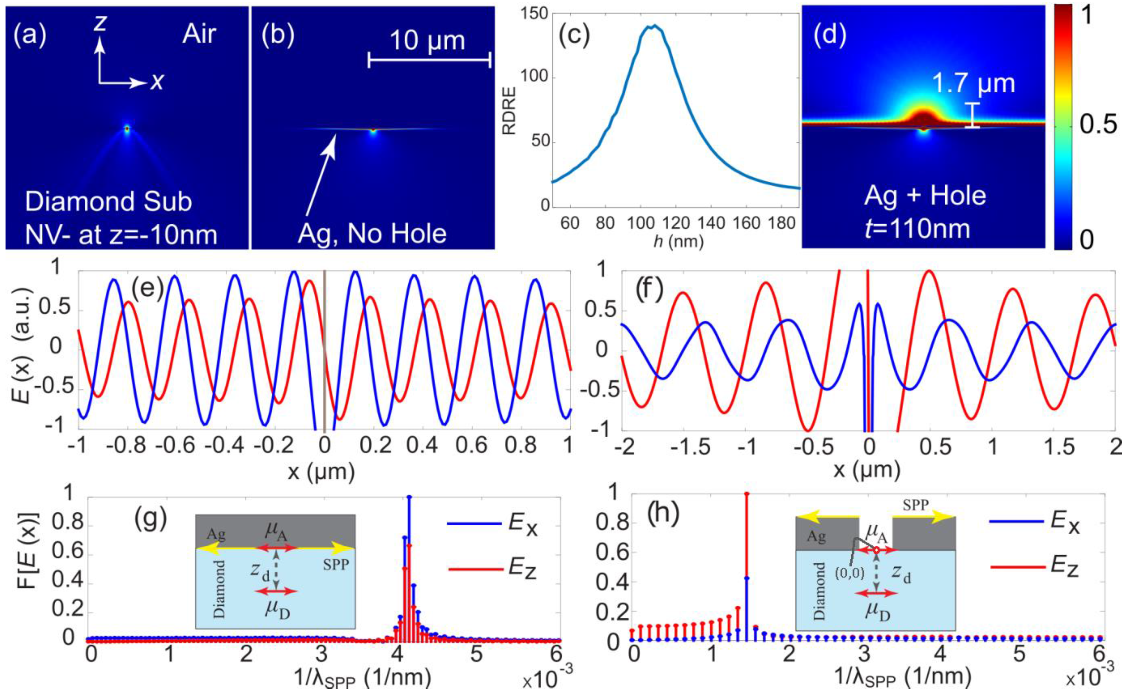
Figure 1a depicts the scattered electric field intensity, |
E|
2, calculated for a diamond membrane with a NV- positioned at (
xd,
zd) = (0, −10) nm with its dipole moment aligned with the
x-axis (i.e., horizontally oriented). The power ratio of
Pair/
Psub ≈ 0.5 is a clear indication that in the absence of any plasmonic structure most of the emitted power is scattered into the diamond. The power ratio
is calculated over a closed arc
s where <
S>
air,sub are the time averaged Poynting vectors calculated in the air and inside the diamond substrate respectively. Introducing an optically thick silver film on top of the diamond substrate reduced the scattered power into the air to ~0, see
Figure 1b. Electric field components, (
Ex,
Ez), calculated over the diamond/silver interface,
Figure 1e, with their corresponding Fast Fourier Transforms (FFT),
Figure 1g, revealed the presence of surface waves, having a wavelength
λSPPd = 230 nm. This agrees with the Surface Plasmon Polaritons (SPP) wavelength
λSPPd = 246 nm obtained analytically using
at
λ0 = 700 nm, where
k0 is the free space wavenumber,
εm and
εd are relative permittivities of the metal and dielectric respectively. It is apparent that some of the emanating power from the dipole is consumed in launching SPPs. Presence of a dipole-like activity associated with a metallic slit has been reported previously [
35]. Therefore, by introducing a resonant aperture perforating the film just above the NV-, it is possible establish the dipole-dipole
resonance energy transfer between the NV- and the aperture.
Figure 1c shows the enhancement to the Radiative Decay Rate (
RDREair) in the air half-space vs. the film thickness,
t, when an aperture having a width
wa = 30 nm, perforates the silver film just above the emitter. The
RDREair was calculated for the air half-space using
, where
P0 is the total power emitted by a nano-diamond in vacuum. The diameter of the isolated nano-diamond was also set to 30 nm in all calculations. This is a typical size for a nano-diamond with luminescence properties [
36,
37,
38]. The factor of 0.5 in the denominator is due to
P0 being calculated along the arc length of a full circle, whereas
Pair was calculated over a semicircle in the air half-space. With
zd = 221,210 nm, a maximum
RDREair ≈ 140 was achieved for
t = 110 nm that corresponds to the first Fabry-Pérot resonance of the aperture [
39].
Figure 1d depicts the electric field intensity, |
E|
2, calculated for the diamond/silver/air multilayer with a 30 nm wide aperture perforating the 110 nm silver film just above the NV-. The power ratio
Pair-Ag110nm+hole/
Psub-Ag110nm+hole = 10 is a clear indication that scattered power is preferential towards the air. Calculated energy transfer efficiency between the donor and the acceptor [
21],
ET =
PD→A/(
PD +
PD→A) =
Pair-Ag110nm+hole/(
Pair-noFilm +
Pair-Ag110nm+hole) ≈ 1 was obtained for
zd ≤ −10 nm. Power ratios
Psub-Ag110nm+hole/
Psub-noFilm = 1.5 and
Pair-Ag110nm+hole/
Pair-noFilm = 33, however, suggest that the presence of the silver film with a resonant aperture enhances the reflected power inside the diamond as well as the transmitted power into the air, hinting at a change in the density of states. It is therefore intuitive to infer that
RDREair ∝
PD→A. Radiation pattern of transmitted field, however, is dispersive with 1/
e of its maximum intensity not reaching beyond
z ≈ 1.7 μm along the optical axis, i.e.,
z-axis.
Figure 1d also shows the presence of high intensity evanescent field along the silver/air interface. Electric field components,
Figure 1f, and their corresponding FFTs,
Figure 1h, calculated over the silver/air interface, confirmed the presence of surface waves with
λSPPa = 667 nm which is in agreement with
λSPPa = 682 nm obtained analytically. Although evanescent waves do not contribute to the far-field [
21], it is possible to intercept and scatter them into freely propagating EM waves by introducing periodic surface gratings surrounding the aperture [
40]. Note however, that for a horizontally oriented dipole moment, induced
Ex is an even function of
x whereas
Ez is an odd function. Consequently, any contribution made by
Ez to the scattered fields leads to a destructive interference along the optical axis. Therefore, considering a 2D model,
Ex (with even parity) is the only contributing factor to the far-field intensity along the optical axis.
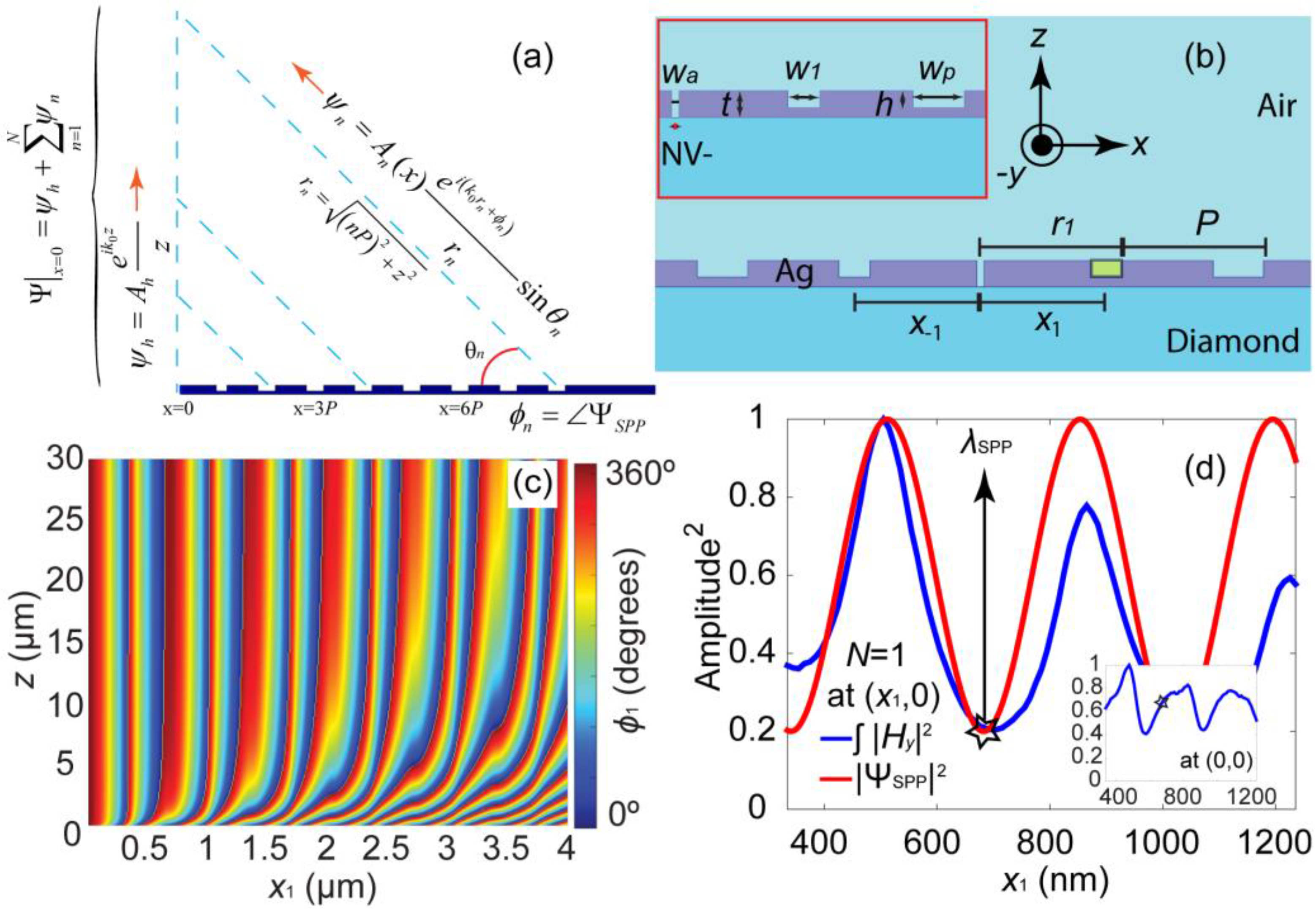
3. Design of Surface Gratings
Detecting the transmitted luminescence of a QE through the aperture, requires reshaping its dispersed radiation pattern into a highly directional light with a maximum possible intensity along the optical axis of a BE structure. Tailoring the exit surface surrounding the aperture with properly designed corrugations is crucial since poor choices may lead not only to the suppression of an already enhanced RDR, but also the formation of side-lobes in the radiation pattern, hence a reduction of transmitted power along the optical axis. Analytical models based on forward propagating SPPs has led to discrepancies between the model and the experimentally observed shortened propagation length attributed to excess losses that required experimentally obtained fitting parameter to correct the theory [
41]. It can be shown, however, the shortening of the propagation length is due to the superposition of surface waves. Relation governing the EM waves along the optical axis of a BE structure consisting of a hole surrounded by
N periodic corrugations with periodicity
P, may be described by:
where
is the wave with an amplitude
Ah emanating from the hole in the
z-direction,
is the scattered wave by the
nth groove having an amplitude
An,
is the distance between
nth groove and an arbitrary point along the
z-axis,
is the phase of the superposed (not just forward propagating) SPP waves at the
nth groove, see
Figure 2a. The role of a corrugation (or a groove) positioned at
xn =
nP, is to utilize some of the power carried by the SPPs to excite LSPs inside the groove,
Figure 2b, whose far-field radiation pattern is similar to that of a dipole antenna. The strength of the LSP inside the
nth groove is denoted by
An. To simplify the argument consider Equation (1) with
N = 1 in a symmetric configuration consisting of an aperture at
x = 0 and a pair of grooves at
x1 and
x−1 with
x−1 = −
x1, where the superposition of SPPs at
x =
x1 may be defined as:
Here, the first term on the right-hand side is the forward wave launched by the aperture arriving at
x1, the second term is the wave launched by the aperture towards
x−1 being reflected back towards
x1, and the third term is the reflected wave from
x1 towards the aperture, being reflected back towards itself. The phase difference between the wave emanating from the aperture and the wave scattered by the groove calculated along the
z-axis,
vs.
x1, showed that for
x1 =
mλSPP/2, Φ → 0 asymptotically only for
z → ∞,
Figure 2c, but
z = ∞ is not a quantitative measure for the far-field. Although matching the period of the corrugations to the SPP wavelength leads to a collimated beam at
z = ∞, simulations confirmed that it did not produce the highest possible intensity along the
z-axis (results not shown here). Therefore, matching the period of the corrugations to
λSPPa is an oversight.
An alternative criterion for maximizing the field intensity along the optical axis is proposed here.
Figure 2d depicts the square of the amplitude of the superposed SPP wave,
, vs.
x1 obtained at the silver/air interface using Equation (2). Note that the square of the amplitude is proportional to the total power available to excite LSPs inside the groove, hence
. This simple configuration was also modelled in 2D using FEM. The numerically obtained magnetic field intensity,
, calculated inside the groove vs.
x1 agrees with the analytical solution. Total power available to the groove follows a Fabry-Pérot like resonance that depends on the groove’s distances from the aperture. The strongest LSP excitation was observed when the groove was positioned at
x1 = 505 nm. The situation becomes further complicated when considering the impact of Fabry-Pérot oscillations on the total power inside aperture, hence the enhancement/suppression of the
RDRair.
Figure 2d (inset) shows that
calculated inside the aperture has its maximum when
x1 = 475 nm and well away from
x1 =
λSPPa, marked by a star.
Given that the aperture and the grooves form an antenna array, as long as their equidistance is less than
λ0, high intensity radiation along the optical axis is guaranteed [
42] (p. 399). But one must also maximize the radiating power available to both the aperture and the grooves. It is intuitive, therefore, to set
x1 to the average of the two peaks mentioned above, i.e.,
x1 = 0.5 × (475 + 505). It is obvious that Equation (2) becomes convoluted for
N > 1. Considering such complex interactions, the only viable approach in designing a BE structure in the presence of a quantum emitter, is to solve the Maxwell equations numerically. With
t = 110 nm and
wa = 30 nm being the optimum values for the film thickness and the aperture width,
r1 was set to
x1 +
w1/2 = 555 nm and a series of parametric sweeps were carried out over each of the remaining parameters
w1,
wp,
h and
P for
zd = −10 nm. In each case, the spectrum for the scattered power into the air vs. the parameter was calculated to identify the peak position that corresponds to the optimum dimension. Note that this is the same approach used in determining the optimum film thickness,
t, see
Figure 1c. One possible configuration, C1, capable of collimating the emission as well as improving the
RDRair was found to be
wa = 30 nm,
w1 = 130 nm,
wp = 210 nm,
h = 70 nm,
r1 =
x1 +
w1/2 = 555 nm,
P = 590 nm and
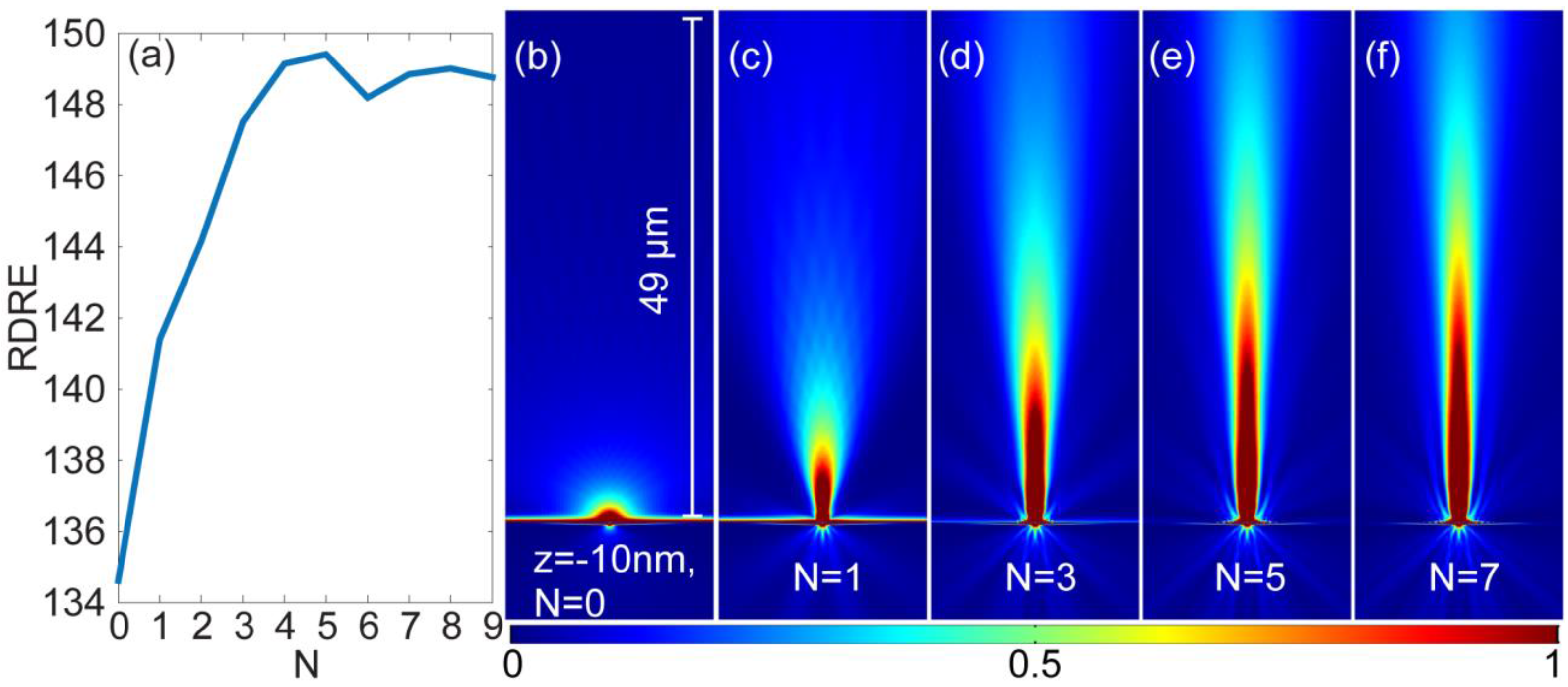
t = 110 nm. Enhancement to the transmitted
RDRair peaks for
N = 5 with no significant changes to the radiation pattern for
N > 5, see
Figure 3. This implies that most (if not all) of the power carried by the SPPs are intercepted and scattered by the first five grooves. Therefore, for the rest of the calculations only 5 grooves are considered. Note that in this report, all 2D field plots are normalized to the same scale and comparable to one another.
With the smallest spot size achievable by an Electron Beam Lithography (EBL) or a Focused Ion Beam (FIB) being as low as ~5 nm [
43,
44], fabrication of the aperture and the surrounding surface features poses no challenge. The resonance energy transfer between the donor and the acceptor, on the other hand, is sensitive to the changes in dipole’s position and orientation. The rest of the report, therefore, is dedicated to study such variations.
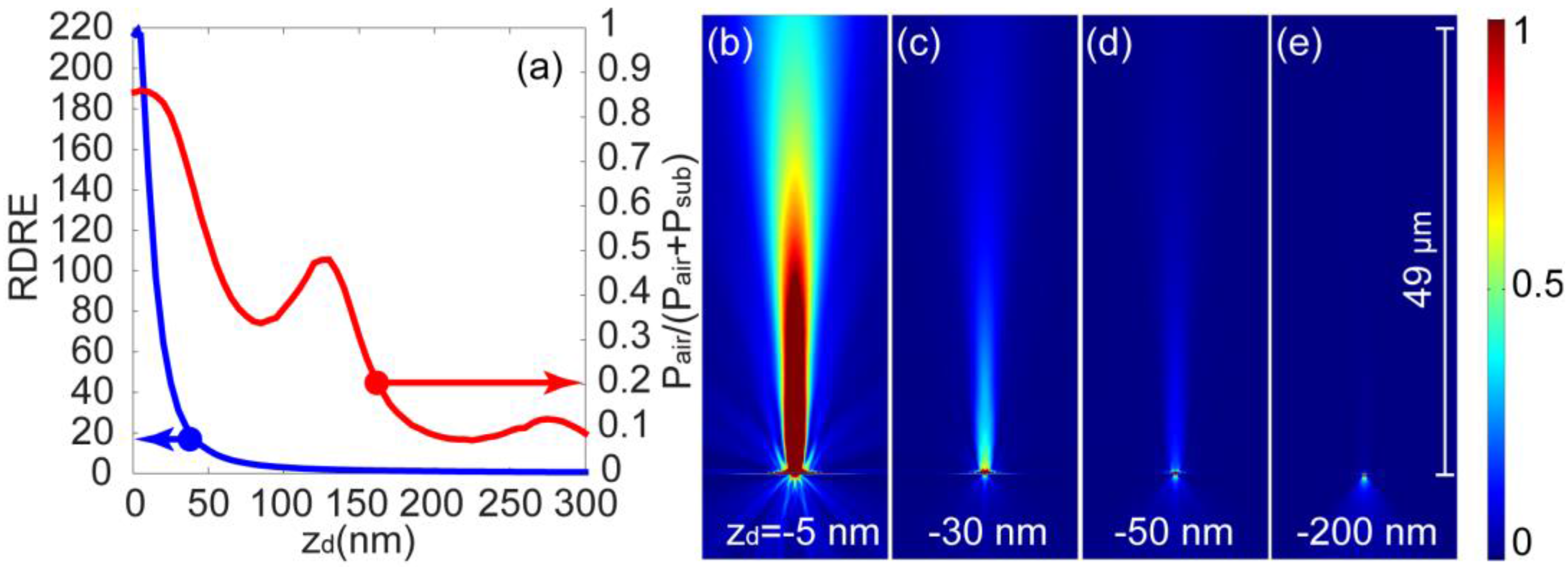
4. Dipole’s Position and Orientation
The transmitted collection efficiency
CE =
Pair-C1/(
Pair-C1 +
Psub-C1) and
RDREair vs.
zd is depicted in
Figure 4a. Note that preliminary investigations with 1 nm steps, revealed the presence of a single peak in
RDREair at
zd = −3 nm. Therefor the resolution for the final parametric sweep over
zd was set to 1 nm in the range of −5 nm ≤
zd ≤ 0 and 5nm for
zd < −5 nm. An enhancement of
RDREair ≥ 216 was achieved for
zd ≤ −5 nm with a maximum of 219 at
zd = −3 nm and a drop to 1/
e at
zd = 17 nm. Rate of change in CE vs.
zd was found to be much slower in comparison to that of
RDREair. A minimum of 80% efficiency in the range of
zd ≤ 25 nm with a maximum of 86% at
zd = −5 nm was obtained. For of a horizontally oriented dipole, transmitted
RDREair showed a reciprocal relation to those corresponding to dipole emissions near flat metallic surfaces. Compare
RDREair spectrum in
Figure 4a in this report to (
P/
P0)
-1 spectrum in Figure 10.5(a) in “Principles of nano-optics” [
21], for example. The slow drop of ~1/
zd0.8 in
RDREair is attributed to the energy transfer between the NV- and the resonant aperture that involves a mutli-channel mechanism. While the direct excitation of LSPs inside the resonant aperture, with its finite cross section, is dominated by short range interactions, the surface surrounding the aperture is able to capture NV-’s emission for longer distances, producing SPPs which consequently couple to the aperture’s LSPs. This slow rate of change with respect to the dipole’s distance from the surface is extremely beneficial. Beaming profiles for few arbitrary
zd values are depicted in
Figure 4b–e.
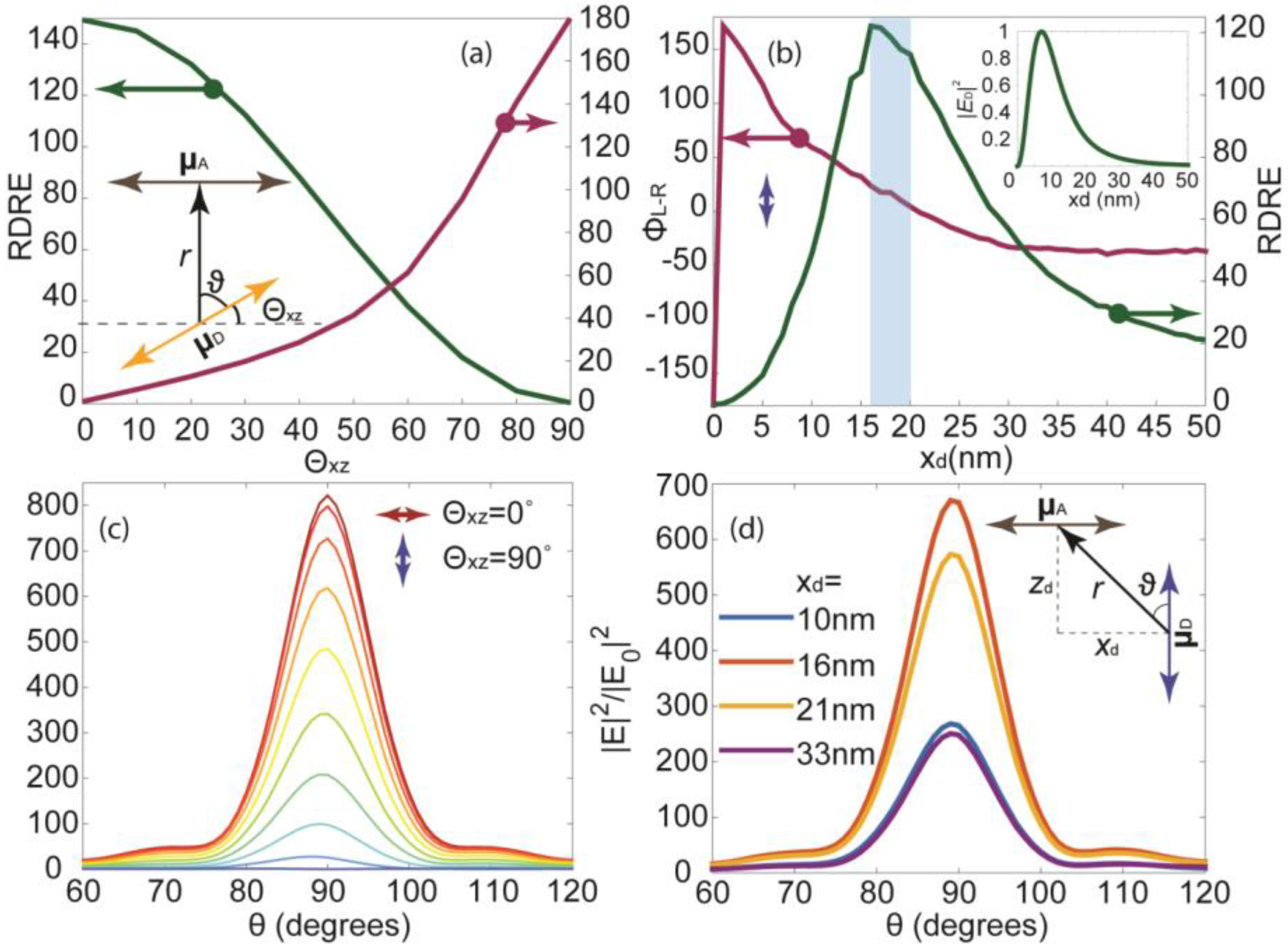
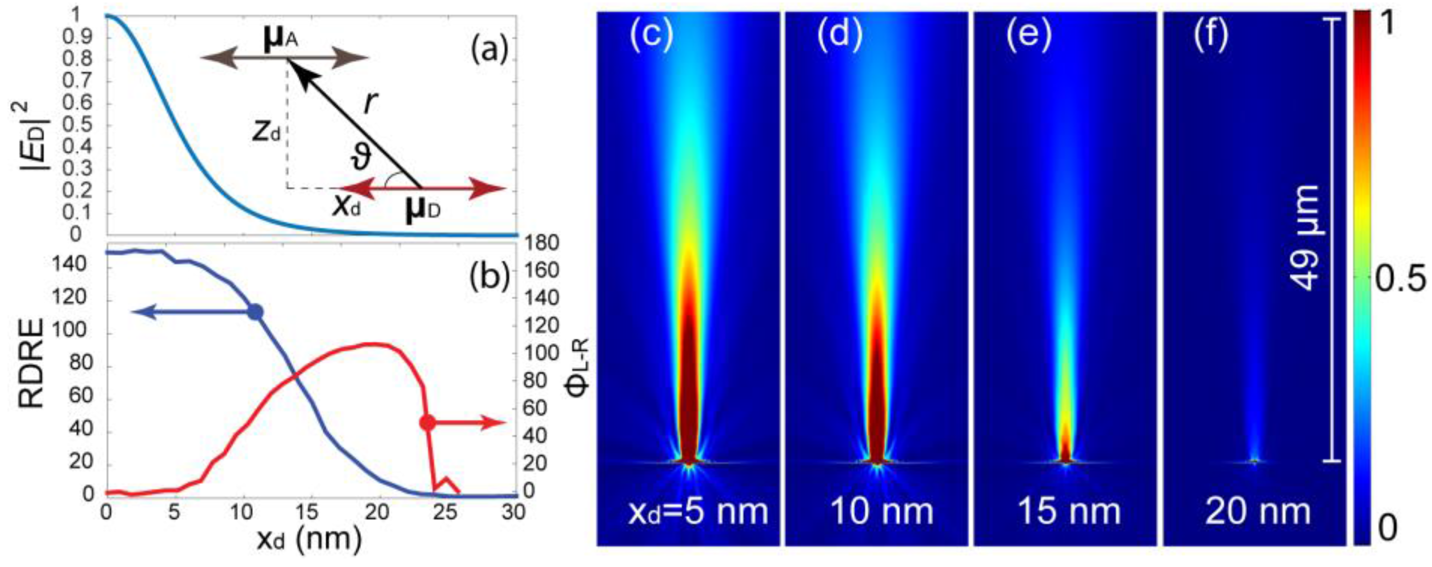
For dipole distances
zd ≤ −10 nm where the near total energy transfer occurs, the donor-acceptor relation between the NV- and the aperture implies that the performance of such a device is sensitive to the donor’s dipolar orientation with respect to that of the acceptor. Retaining only the near-field term, radiation pattern of the donor (i.e., NV-) may be written as [
21]:
where
with
ϑ being the angle between
r and the donor’s dipole moment, µ
D, see inset of
Figure 5a. C1’s response vs. the direction of µ
D in the
x-
z plane was calculated in the range of 0° ≤ Θ
xz ≤ 90°.
Figure 5a shows that the power transfer between the donor (NV-) and the acceptor (aperture) does in fact comply with
PD→A ∝ |µ
A·
ED|
2 [
21], where µ
A is the dipole moment of the acceptor. Consequently, for a vertically oriented µ
D,
PD→A and
RDREair drop to zero. Unlike the simple donor-acceptor interaction observed in florescent molecules, the interaction between the NV- and C1 is influenced by plasmonic effects, therefore surface wave launched by the aperture must also be examined. Numerically obtained phase difference between
Ex oscillations on the corners of the aperture at the silver/diamond interface,
, revealed that Φ
L-R is a function of Θ
xz, and may be defined as
,
Figure 5a. This implies that one can define the parity state of
Ex as
, where
and
are the states of pure even and pure odd parities with probabilities of cos
2(
f(Θ
xz)) and sin
2(
f(Θ
xz)) respectively. For pure
state of
Ex, however, one must not assume that NV’s emission is quenched. It can be demonstrated that for a vertically oriented µ
D a small displacement in its horizontal position with respect to the center of the aperture, not only overcomes the suppressed
PD→A, but also causes the transition from the odd to even state,
, hence satisfying the two mandatory conditions for a high intensity constructive interference along the
z-axis. Numerical results depicted in
Figure 5b confirm that for 16 ≤
xd ≤ 20 nm both conditions are satisfied. The trend observed in the
RDREair spectrum is due to the donor’s projected field intensity over the aperture, |
ED|
2(x=0,z=0), varying with
xd. Analytical values for |
ED|
2(x=0,z=0) vs.
xd were calculated using Equation (3), with sin
ϑ = |
xd|/
r, see
Figure 5b (inset). Although, Equation (3) does not take into account the aperture’s dimension, reflection terms and interactions with surface waves, the trend in |
ED|
2 spectrum agrees with that obtained numerically for
RDREair. Directional gain of the BE antenna, |
E(
θ)|
2/|
E0(
θ)|
2, vs. Θ
xz is depicted in
Figure 5c. The field intensity along the optical axis can be 800 times that of a free standing nano-diamond when Θ
xz = 0°. Here |
E(
θ)|
2 and |
E0(
θ)|
2 are the electric field intensities as a function of angle,
θ, from the
x-axis calculated for C1 and a nano-diamond particle in vacuum respectively. FWHM of the beam remains approximately 14° for all Θ
xz values. Corresponding directional gains vs.
xd = {10, 16, 21, 33 nm when Θ
xz = 90° are shown in
Figure 5d. The angle
θ, may be expressed in terms of Θ
xz,
xd and
zd as:
, valid in the range of 0° ≤ Θ
xz ≤ 90° and
xd ≥ 0.
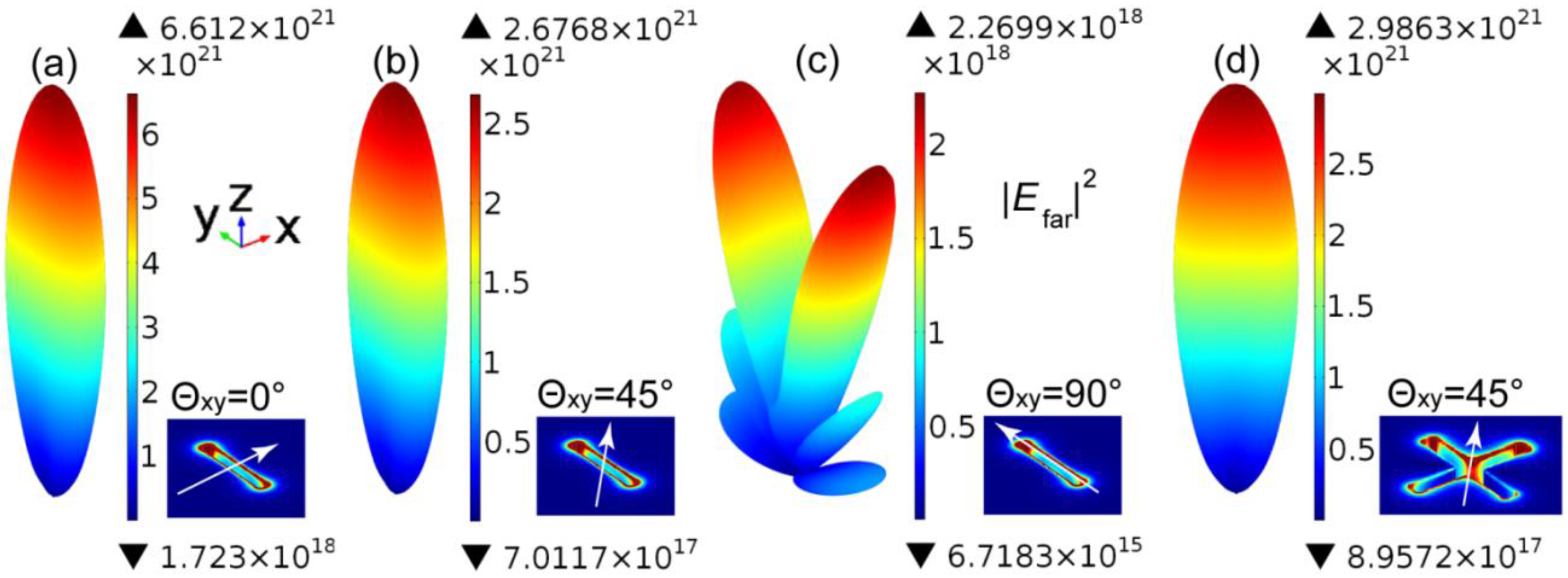
Previously, it was shown that the
xz (or
yz) plane of experimentally obtained volumetric radiation patterns of a bullseye structure, corresponds to the radiation pattern of a simulated 2D grating [
22] (see Chapters 8, 9 and Appendix A). To evaluate C1’s response vs. the change in
µD in the
xy plane, C1 was first modelled in 3D as a BE structure with a 250 nm long slit and later with a symmetric cross-shaped aperture having the same arm-lengths. The spherical simulation domain was divided by the planar structure into two hemispheres, with the bottom being the diamond substrate and the upper being the air. The first Fabry-Pérot resonance of the aperture in both cases occurs at
t = 130 nm. To reduce the required computational resources, number of corrugations were limited to
N = 3. All other dimensions were kept in accordance to the 2D model. A parametric sweep over the orientation of
µD in the
xy plane, Θ
xy, showed that
RDREair ∝ |
µA·
ED|
2 for the slit, as anticipated.
RDREair in 3D was calculated using
with integrations being carried over the surface
s enclosing the hemisphere. The maximum
RDREair obtained from the 3D model was calculated to be ~100 (results not shown here). Far-field intensities, |
Efar|
2 vs. Θ
xy also followed a similar trend with collimated beams being achieved for Θ
xy < 90°,
Figure 6a–c. Far-field intensity emanating from the symmetric cross-shaped aperture, on the other hand, was impervious to the change in Θ
xy but the maximum far-field intensity in this case was almost half of that achieved by the slit, i.e., |
Efar-cross|
2/|
Efar-slit|
2 = 0.45 at their respective maxima. Presence of an additional arm in the cross-shape aperture reduces the nearby metallic surface area over which |
ED|
2 is projected on to, hence the reduction in absorption cross section of the acceptor.
For a horizontally oriented
µD, field amplitude of the donor projected over the aperture vs.
xd was calculated analytically using Equation (3) with sin
ϑ = |
zd|/
r, see
Figure 7a. The trend observed in |
ED|
2(x=0,z=0) spectrum agrees with that of the
RDREair obtained numerically,
Figure 7b. Numerical results revealed that the device tolerates a lateral displacement of Δ
xd ≈ ±15 nm beyond which the
RDREair drops below 1/
e of its maximum. The phase difference ΔΦ
L−R in this case rises at
xd ≥ 7 nm, reaching a maximum of ~105° at
xd = 23 nm but never attaining a 180° difference to qualify
Ex as a pure odd function.
RDREair, on the other hand, drops to 1/
e of it maximum at
xd ≈ 15 nm where ΔΦ
L−R is 70°. Defining the state of even function-ness as cos
2(ΔΦ
L−R/2), a 70° phase difference must drop the
RDREair only to 0.67 (not 1/
e) of its maximum. The 55% excess reduction, therefore, is partially due to the
Ex not being a pure even function and partially due the reduction in |
ED|
2(x=0,z=0) with increase in
xd.
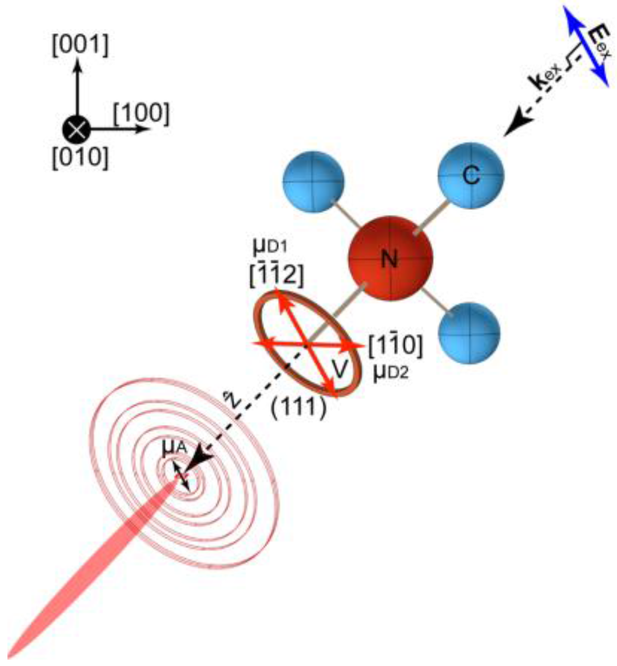
5. Crystallographic Directions
From all possible dipole orientations considered in this report, it can be inferred that a horizontally oriented
µD with a plasmonic slit offers the best outcome with the highest
RDREair and tolerance. Descriptions on triplet notations and Miler indices used in crystallography, may be found in undergraduate solid state texts [
45,
46]. With NV- symmetry axis being one of the <111> crystallography directions [
26,
27], one may narrow the search for a horizontally oriented
µD. Assuming that the planar design lies on an arbitrary plane, z, defined by its normal vector
, possible scenarios are (a)
z plane parallel to diamond’s
plane which implies that
µD is parallel to the
direction, hence the slit must be fabricated such that
µA ‖
µD. To maximize the emission from the NV- in this case, the excitation field,
Eex, must also be polarized in the
direction; (b)
z plane ‖
with
Eex ‖
µA ‖
µD ‖
; (c)
z plane ‖ 111) (or
being aligned with the symmetry axis of the NV-) with no preferential direction for neither
Eex nor
µD since
µD =
α2µD1 +
β2µD2, where
α2 +
β2 = 1, see
Figure 8. Depending on the application, one can identify other diamond planes over which the planar structure to be set. For examples: if the emphasis is on the extraction of single photons, then the diamond plane must be chosen such that (
µA ‖
µD1 AND
µA ⊥
µD2) OR (
µA ‖
µD2 AND
µA ⊥
µD1). On the other hand, if one is to investigate the two-entangled photon arising from the mutual excitations of
µD1 and
µD2, then it is best to implement the planar structure using a symmetric cross aperture on the (111) plane with the arms of the cross being aligned with
and
.

