Integrated Microwave Photonics for Wideband Signal Processing


1
School of Electrical and Information Engineering, The University of Sydney, Sydney, NSW 2006, Australia
2
Australian Institute for Nanoscale Science and Technology, The University of Sydney, Sydney, NSW 2006, Australia
*
Author to whom correspondence should be addressed.
Photonics 2017, 4(4), 46; https://doi.org/10.3390/photonics4040046
Submission received: 1 November 2017
/
Revised: 24 November 2017
/
Accepted: 24 November 2017
/
Published: 30 November 2017
(This article belongs to the Special Issue Microwave Photonics 2017)
Abstract
:We describe recent progress in integrated microwave photonics in wideband signal processing applications with a focus on the key signal processing building blocks, the realization of monolithic integration, and cascaded photonic signal processing for analog radio frequency (RF) photonic links. New developments in integration-based microwave photonic techniques, that have high potentialities to be used in a variety of sensing applications for enhanced resolution and speed are also presented.
1. Introduction
The quest for greater speed, bandwidth, and reconfigurability has led to an active pursuit in the field of microwave photonics (MWP) for the generation, transmission, and processing of radio frequency (RF) signals in the optical domain. While initially, defense and radar applications were the main beneficiaries of this technology, the scope has since expanded to encompass many new areas of developments. Bringing together the worlds of radiofrequency (RF) engineering and optoelectronics, the field of MWP has recently attracted great interest from both the research and the commercial communities where its importance has been identified in emerging applications including medical imaging, future 5G networks, and subterahertz systems. It offers the unique abilities to enable key functionalities in microwave systems such as filtering, arbitrary waveform generation, frequency up/down conversion and instantaneous measurement that are either complex or even not directly possible in the radiofrequency domain [1,2,3,4,5,6,7,8,9]. As the role of MWP develops from niche to widespread applications, it becomes important to replace systems that rely exclusively on discrete optoelectronic devices and fiber-based components. These systems are bulky, expensive, and power-hungry, making them economically unfeasible to be mass produced for a widespread use. The challenge has thus intensified to implement reproducible, compact, lightweight, low power consumption and low-cost MWP systems that are physically and economically competitive against their electronic counterparts. This calls for an evolution of MWP components in the form of integrated circuits which aims to incorporate many devices and optical functionalities on a single photonic chip to achieve high speed and wideband signal processing functions [4,5,6,7,8,9].
The area of integrated MWP signal processors has been a tremendously active area of current research and development, and is the technology best positioned to realize compact versions of existing MWP systems with similar or even better performance. Work in this field has attracted a great deal of attention in recent years and has been reported by several groups spanning various platforms such as silicon photonics [5,6,7], III–V semiconductors [8], and Si4N3 (TripleX) technologies [9].
In this paper, we present recent new developments in integrated microwave photonic signal processing with a focus on the key signal processing building blocks for RF systems and photonic links, which include an integrated microwave photonic phase shifter, time delay line, and frequency tunable microwave filter for amplitude control. Finally, we will give a broad view on the realization of these full functionalities from a system link perspective of a general-purpose MWP system. Specifically, the future of inline photonic signal processing systems with cascaded functionalities and the potential approaches for realizing full platform integration of MWP systems will be discussed. The attractive use of MWP techniques such as optoelectronic oscillators (OEO) for sensing applications is also explored. We present the prospects of transferring these OEO technologies onto an integrated platform with a demonstration of an on-chip sensing probe for enhanced resolution and interrogation speed. Because of the vast scope of research in this area and the high volume of publications, we would like to point out that this paper, although covering a wide range of integrated MWP, will not provide an exhaustive list of published papers in the field.
2. Integrated MWP Phase Shifter
Microwave phase shifting plays a central role as one of the key components making up the backbone of a wide range of signal conditioning functionalities such as programmable filters [10] and phased-array beamforming networks for radar, defense, and satellite communication systems [11,12]. In contrast with traditional microwave phase shifters which are typically limited by their electrical bandwidth, tuning speed, and phase shifting range, the use of photonic techniques to perform RF phase manipulation has been a popular area of research where the appeal of employing MWP phase shifters lies in the expansion of the bandwidth potential and high speed configurability which is often difficult to achieve using purely RF components.
The exacting requirements of microwave phase shifters demand not only the ability to provide a full, tunable range of 0–360° phase shifts but also to have the ability to operate over a wide bandwidth while introducing minimal RF power variations. Phase shifters based on the use of various discrete photonic components such as 2D liquid crystal on silicon [12], stimulated Brillouin scattering (SBS) effect in optical fibers [13], vector sum [14], optical filters [15], semiconductor optical amplifiers [16], fiber Bragg gratings (FBGs) [17], and electro-optic modulators [18,19,20], have been demonstrated.
Exploring the direction of nanophotonics, several platforms have already been identified as promising solutions for implementing integrated MWP phase shifters. Silicon photonics has been widely investigated due to its complementary metal-oxide-semiconductor (CMOS) compatible nature which allows silicon based MWP phase shifters to be seamlessly integrated together with electronic circuits [21,22]. The development of phase shifter structures also enables the achievement of high performance MWP phase shifting functions. On-chip integrated MWP phase shifters based on silicon-on-insulator (SOI), where the high index contrast allows for an extremely compact footprint for key components such as ring resonators, have been demonstrated by using a single ring resonator [22]. The phase shifter operation shows a continuous RF phase tuning from 0 to 270°, as depicted in Figure 1a. The corresponding RF amplitude response of the MWP phase shifter is shown in Figure 1b. The inset of Figure 1b illustrates the optical response of the phase shifter which was measured by using an optical analyzer (Finisar Wave Analyzer), showing a notch depth of approximately 7 dB at the resonance location. As the MWP phase shifter is implemented based on a single microring configuration, the RF power variation due to the high extinction ratio of the microring filter can be minimized by reducing the loss of the microring and optimizing the coupling coefficient between the straight waveguide and racetrack waveguide [23]. Moreover, the use of cascaded microring resonators to implement phase shifting can also be adopted to enlarge the phase shifting range and present a more controllable RF power variation [24].
Other platforms with integration potential involve silicon nitride [9] and charcolgenide waveguides [25]. The further investigation of new platforms has also aided in the discovery of graphene based waveguides [26] which provides tunability with relatively low electrical energy and PbS colloidal quantum dot based waveguide [27], which displays fast tunability. Recently, aluminum nitride [28] which exhibits second order optical nonlinearity has also been explored to implement ring resonator based phase shifters with increased phase tuning speed. Moreover, it has been demonstrated that different platforms can be integrated through heterogeneous integrated technology [29], which provides additional flexibilities.
3. Integrated MWP Delay Line
Optical delay lines, which delay an optical signal by a selected increment of time, play a key role in the implementation of a variety of microwave photonic signal processing functionalities [30,31]. For example, one important application is optically controlled beamforming for phased array antennas, where the delay element is an essential component for compensating the frequency dependency of beam direction, or beam squint effect.
Non-resonant delay lines are of great interest due to their ability to form a large time delay as well as a wide operating bandwidth. Thanks to the CMOS-compatible fabrication technology which promises a more cost effective, robust and compact solution, delay elements based on various chip-scale platforms have been intensively investigated. In particular, low propagation loss has been demonstrated in optical waveguides of wedge geometry, high-aspect-ratio Si3N4, and high-quality silicon oxynitride films [32,33,34,35,36]. In [32], an optical delay line fabricated on a silicon chip has been presented, exhibiting an average measured waveguide loss of 0.08 ± 0.01 dB/m in long spirals.
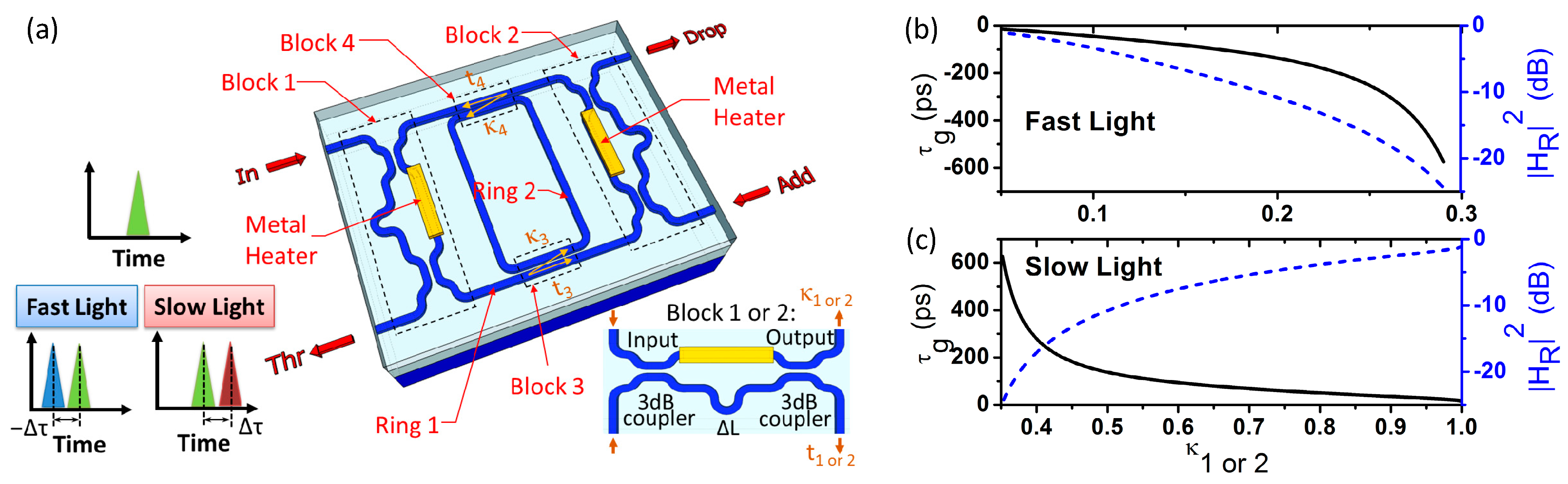
Employing resonance behavior of the whispering-gallery-mode [37,38] and microring cavities [39,40,41,42,43] forms another class to realize time delay functions. To extend the operating bandwidth of the delay lines, multiple microring resonators cascaded in versatile topologies such as coupled resonators optical waveguide (CROWs) [39,40,41,42], and side-coupled integrated spaced sequence of resonators (SCISSORS) [40] have been proposed. In [43], an optical delay with high bandwidth and continuous tunability was achieved by employing microring resonators in a balanced SCISSORS configuration. A 10 GHz operating bandwidth using thermally tuned silicon microring resonators was experimentally demonstrated. Microring resonators in an eye-like configuration as a continuously tunable delay line has also been reported [44]. The eye-like delay line unit consists of the outer (Ring 1) and inner (Ring 2) racetrack resonators as shown in Figure 2a, where the group delay exists at the through port of the unit. The optical power in Ring 1 is partly coupled between the bus waveguides by the temperature-controlled Mach Zehnder Interferometer (MZI) power splitters in Block 1 and 2, and also Ring 2 by the static directional couplers in Block 3 and 4. The temperature-controlled MZI power splitters are regarded as the tunable coupling devices such that the tunable coupling ratios κ1 and κ2 are obtained in Block 1 and 2, respectively. The dependences of group delays on coupling ratios are plotted in Figure 2b,c. The analysis is conducted on the eye-like resonator with the outer ring circumference of 397 µm which occupies the space smaller than 0.019 mm2. With the temperature-controlled MZI power splitter between the resonator and the bus waveguides, the eye-like resonator based delay line can be operated in over-coupling and under-coupling regimes. It should be noted that a considerable delay of 627 ps can be achieved in the over-coupling condition while maintaining the optical loss less than 25 dB. Optical delay lines can also be realized via adopting a series of Mach Zehnder Interferometer (MZI) or microring resonator-based optical switches, thus generating a tunable time delay controlled by the optical path change [45,46,47,48]. In [48], for example, a delay element based on microring resonators in combination with graphene-based Mach–Zehnder interferometer switches is reported on a silicon nitride platform, demonstrating an optical delay up to 920 ps with optical loss less than 27 dB.
4. Integrated MWP Filter
Filtering of microwave signals in the optical domain provides the means to achieve fast re-configurability with direct ease, which also enables flexibility to operate at high frequencies while achieving a wide tuning range [51]. Such dynamic filtering performance is essential in applications such as radar and surveillance where RF disturbances are very likely to occur at random frequencies [2,52,53]. The ability to provide continuous tuning for arbitrary frequencies allows the system to adapt to the constant changes in the front-end operational requirements, where achieving such performance in the electronic domain still remains a challenge.
There are three main approaches categorizing MWP filters. One method of implementation builds upon the configuration of finite-impulse response (FIR) filters, which makes use of the summation of a number of time-delayed and weight tailored multi-wavelength optical taps to generate the RF output at the photodetector end [54]. The high programmability of such filters which permits agile controllability and reshaping capabilities have spurred an invigorated drive to replace fiber and bulky optics devices with integrated based components. Immense effort has since been put into investigating on-chip programmable filters based on this approach. These have been successfully demonstrated on various integrated platforms such as InP-InGaAs, SOI and hybrid silicon [55,56,57]. The FIR based scheme being discrete in nature, however, exhibits a periodic transfer function, which gives rise to the presence of multiple harmonic passbands within the spectral range of interest [4]. Recognizing the limitation this poses on the rejection range of unwanted frequencies, a single passband can be achieved by combining optical and RF filtering techniques to eliminate all the unwanted periodic passbands arising from structures based on a discrete multi-wavelength optical source [58].
The second category is based on the direct filtering method, where phase modulation to intensity conversion is used to directly map the response of an optical filter to reflect a single RF passband MWP filter in the electrical domain [59,60,61,62]. The simplicity of this method allows for the direct manipulation of the RF amplitude response and permits the execution of continuous tuning of the RF passband with a high resolution. A broader operational bandwidth without spectral overlapping is achieved, where the undesired multiple harmonic passbands caused by the discrete time nature in FIR filters is eliminated. High extinction ratios for rejection of unwanted RF signals can be achieved with optical filters exhibiting very narrowband optical response such as phase-shifted FBG [59], a pair of FBGs [60], optical bandpass filters [61], and Brillouin selective sideband amplification [62,63].
Finally, infinite impulse response (IIR) integrated optical filters based on SOI microring resonators have been used to demonstrate their feasibility in implementing single passband MWP filters [64,65]. The resulting RF filters show 3-dB bandwidths of several GHz, and sideband suppression of less than 10 dB in [64] and 12 dB in [65], respectively. In [50], a tunable and reconfigurable MWP filter based on a highly dispersive, low-loss 1.55 mm-long PhC waveguide delay line, which is characterized by an anti-symmetric shift of the first row of holes, has been presented. A tuning capability over the 0–50-GHz spectral band and a broadband operation bandwidth up to 50 GHz have been demonstrated for both notch and band-pass microwave filters. Whilst photonic integrated circuit technology has made it possible to realize compact and lightweight photonic devices, the miniaturization of photonic components also render them susceptible to fabrication mismatch, thus making it challenging to cascade devices for very high Q integrated optical filters. Moreover, the resulting MWP filter typically suffers from degradation in the extinction ratio of the filter passband due to the additional phase variations introduced by the optical filter onto the carrier and sidebands. As a result, the amount of cancellation in the phase-to-intensity modulation conversion process is far from ideal.
To overcome the RF distortion induced by the unwanted phase variation, a phase compensated SOI microring resonator topology was proposed [66]. The proposed structure was able to reduce the phase variation over the bandpass region of the notch filter thus achieving a RF filter response with an improved sideband suppression of over 20 dB while exhibiting a wideband frequency tuning range between 5 GHz and 40 GHz and high selectivity with a 3-dB bandwidth of just above 1 GHz. However, as the proposed technique requires the use of a discrete phase compensator, this prevents the system from being fully integrated. In order to overcome this limitation, a new technique has been proposed which is based on an integrated double microring resonator configuration to enhance the selectivity of the RF passband filter as shown in Figure 3 [67]. This novel concept allows the realization of an RF filter whose bandwidth is directly related to the difference in bandwidths of the two unequal optical notch filters. This fully integrated approach simply uses a cascaded pair of microring resonators with slightly different bandwidths to enhance the selectivity of the single passband microwave photonic filter (SPMPF). As the 3 dB-bandwidth of the resulting SPMPF is not governed by the absolute bandwidth of a single optical filter, precise tuning of the device to achieve high Q resonator-based filters in critical coupling condition can be avoided. Experimental results have demonstrated a SPMPF with an improved out-of-band suppression ratio of around 20 dB, as well as a wide and shape invariant tuning of the SPMPF showing continuous tuning capabilities from 6 GHz to 17 GHz by using a fixed wavelength laser. The filter bandwidth was kept to less than 1.9 GHz while maintaining the shape factor under 1.78 with a maximum variation of only ±0.05 throughout the entire tuning range.
One strategy to maintain the fidelity of the processed radiofrequency (RF) signal is by implementing rectangular MWP filters which are characterized by their flat-top passbands. A few schemes have been reported to obtain microwave photonic filters with flattened passband such as directly synthesized complex impulse response technique [68], spectrally shaping the optical pump source in SBS-based filters [69] or elaborate programming of FIR filters to construct a flat-top passband [70]. To aid the implementation of MWP filters with flat passband characteristics on an integrated platform, new synthesis methods to design integrated optical filters with flat top characteristics based on multiple stages of stagger-tuned microring resonator filters have also been proposed [71]. Integrated optical filters with a flat-top can also be utilized to achieve the desired rectangular MWP filter response via direct filtering method [72].
The concept of using integration based RF filtering for amplitude control can also be extended to other applications such as the fifth generation (5G) mobile communication network to lower the cost of deployment of radio-over-fiber (RoF) based networks. For example, in [73], an analog 60 GHz RoF fronthaul link employing integrated MWP filters was presented to provide a compact and low-cost optical filtering solution. In the proposed fronthaul link, a SOI ring-based dual-passband optical filter was presented to enable the transmission of millimeter wave radio signals.
5. Integrated MWP for Optical Sensing Applications
In traditional optical sensing systems, where a change in the sensor measurand is converted into a shift in the optical sensing resonant wavelength, an optical interrogator such as an optical spectrum analyzer is required to convert the wavelength shift into an electrical signal. This, however, raises the issues of sensitivity and speed limitations. In contrast, sensors based on microwave photonic signal processing techniques can conveniently convert the change in the optical domain to a corresponding variation in the microwave domain. The ability to perform measurements in the RF domain, which provides higher frequency resolution, enables a superior method for high resolution monitoring of miniscule changes in the measurand, thus enabling high performance sensing [74]. A much higher interrogation speed can also be obtained since the microwave frequency can readily be measured by a digital signal processor (DSP) with high speed and high resolution. One technique to implement the interrogation of optical sensors is via an optoelectronic oscillator (OEO) system, which is an important system for microwave photonics that enables the generation of high-frequency and stable microwave signals by combining the unique advantages of electronic and photonic components [75,76].
The conventional optoelectronic oscillator structure requires an electrical bandpass filter in an optoelectronic feedback path to select the desired oscillation frequency. However, the low-frequency operating range and limited tunability of typical electronic filters impose restrictions on the bandwidth, noise and stability of generated oscillations, making these optoelectronic oscillators unsuitable for high-frequency applications. To overcome this fundamental limitation, MWP filters based on the direct filtering method can be employed to replace electronic filters. Using these optical filtering devices as the sensing probe, the microwave oscillation frequency can be determined by the resonant wavelength of the optical device. However, the practicality of current OEO-based sensor schemes, which are typically comprised of bulk components of large physical size, is limited. The challenge is now to transfer the OEO-based topologies onto an integrated platform in order to develop compact and portable solutions for sensing environment variables.
The first steps to developing an integrated OEO-based system was first initiated in [77] where we presented an integrated photonic sensor based on an optoelectronic oscillator with an on-chip sensing probe that is capable of realizing high sensitivity and high resolution. This work engaged the use of a SOI microring resonator to continuously select different RF oscillation modes. As an application example, the targeted measurand was chosen to be temperature. Figure 4a shows the working principle of the proposed OEO based optical sensor that employs an integrated microring resonator as the sensing probe element. The chip was placed under a heat sink with temperature controllability provided by a thermoelectric cooler (Newport) to emulate the effects of disturbance in the ambient temperature. The frequency response of the generated electrical signal at 24.78 °C is shown in Figure 4b, which depicts an electrical signal at 14.3 GHz. The inset of Figure 4b shows the zoomed in response which illustrates a narrowband signal with a linewidth of 0.1 MHz. The next most dominant mode is located at 4.9 MHz away from the peak oscillation mode and shows a mode suppression of 30.6 dB. To investigate the temperature sensing performance, the temperature of the nanochip sensor was varied from 24.27 °C to 25.29 °C. Figure 4c shows the superimposed spectra of the generated microwave frequencies at different temperature points. As the temperature increases, the signal is shifted to a higher frequency where a linear relationship is formed between the temperature change and RF frequency shift, as shown in the linear fit in Figure 4d. The linear dependence of the frequency shift on temperature is estimated to be around 7.7 GHz/°C, thus demonstrating its high sensitivity.
6. Integrated MWP for Inline Photonic Signal Processing and Full Platform Integration
The proliferating interest in low-cost, compact MWP subsystems has continued to push the boundaries of scalability to develop multi-functional MWP subsystems. A majority of the existing MWP systems were designed to be implemented as stand-alone systems which are segregated according to different key signal processing functionalities such as RF amplitude manipulation, delay line, and phase control capabilities. The challenges arises when the same system is expected to incorporate an additional signal processing function. For example, in radar applications where the system may not only need to perform RF phase shifts to steer the signal in a specified direction but it may also need to concurrently reject unwanted out-of-band interference via RF filtering.
To achieve a multi-functional MWP signal processor, the direct cascade of multiple MWP subsystems is a possible option. The MWP link should be efficiently utilized to its fullest potential and have the ability to handle a variety of functionalities. In microwave fiber-optic systems where the signal is already in the optical domain, it is thus attractive to continuously process the signal directly in the optical domain itself, thus eliminating the unnecessary rounds of conversions between the electrical and optical domain of the individual functions. For photonic chips to be on a competitive edge over their electronic counterparts from an economic and practical standpoint, a radically different approach needs to be considered to establish the means to realize a distributed variety of functionalities within a single MWP link.
A practical MWP signal processing system that combines the cascaded usage of different optical signal processing subsystems into one compound MWP system was proposed [22]. The novel photonic link with distributed functionalities is capable of performing separately controlled, cascaded microwave bandpass filter and on-chip phase shifter functions. This demonstration is relevant to radar applications, for example in RF phased array antennas [15]. Meanwhile, highly selective frequency filtering in multioctave radar systems with tuning capabilities is also needed to suppress and adapt to the constant change in the unwanted out-of-band interferences.
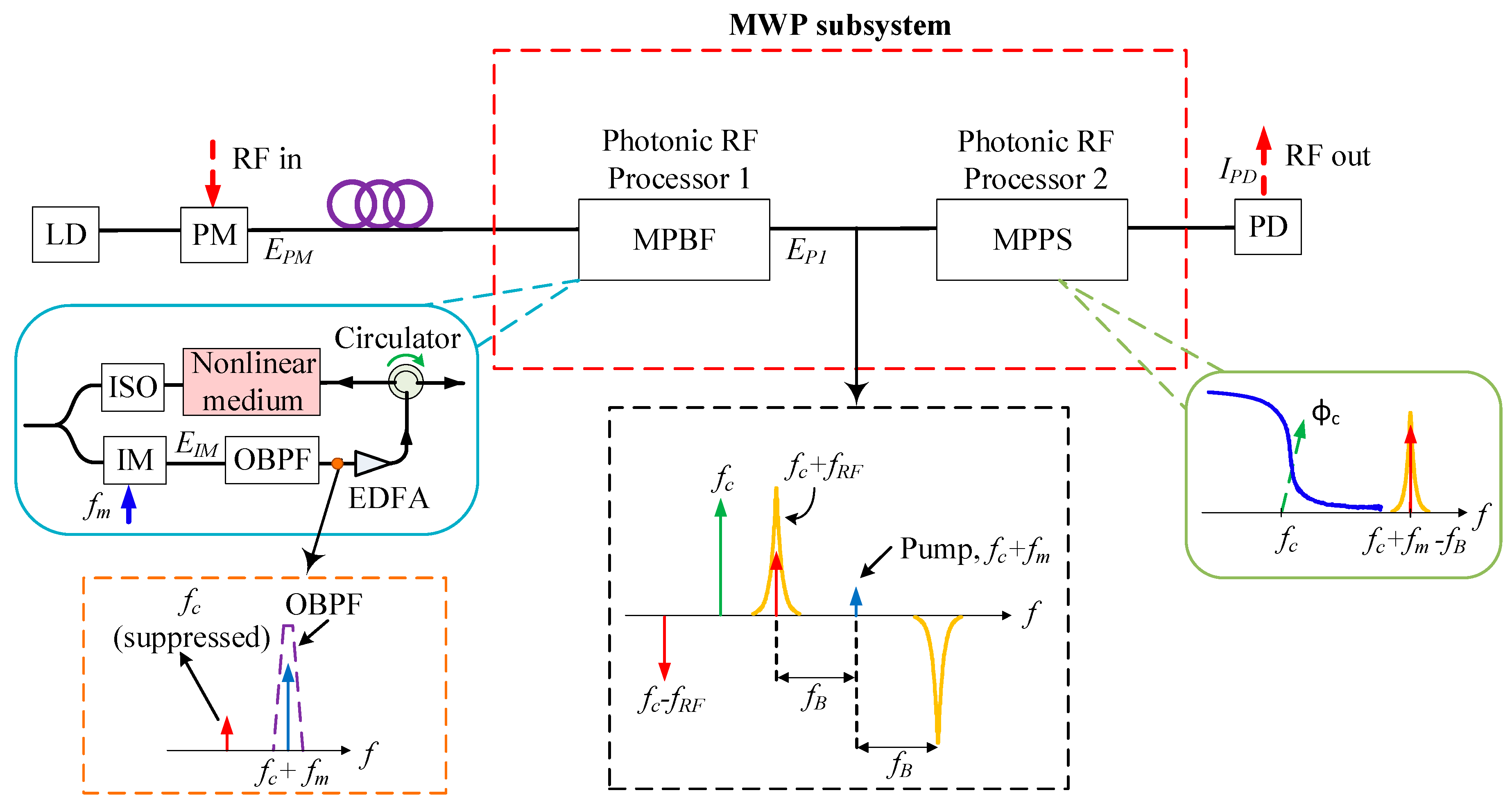
As shown in Figure 5, the proposed system configuration in [22] cascades a SBS based MWP bandpass filter and an on-chip phase shifter based on a single all-pass microring resonator. In order to preserve the independent functionality of each subsystem, a new SBS configuration was utilized to support the cascaded signal processing functions which is otherwise not achievable using conventional structures. In contrast with previous implementations of the SBS-based filtering function where a pure optical carrier derived directly from the source laser was used as the pump signal, the new system adopts the concept of re-modulating the transmitted phase modulated light in the lower arm of the first signal processor via an intensity modulator (IM). The reused modulated optical carrier can then be continuously frequency shifted and filtered to act as a tunable pump signal. The tunability of the MWP filter passband is realized by tuning the optical pump driven by an external RF source generator. The RF signals within the SBS amplification profile is then transmitted together with the optical carrier along the MWP subsystem to the next stage of signal processing, which comprises the MWP phase shifter. Due to the selective amplification of the RF signals from the previous stage, the optical signals at this stage can be viewed as a narrow array of single sideband RF frequencies. Therefore, a phase shifter based on an optical single sideband modulation format can conveniently provide a one-to-one mapping of optical to RF phase shifts. The carrier wavelength is aligned with the resonance of the phase change induced by the MWP phase shifter so that an optical phase change is induced at the optical carrier. The tunability of the MWP phase shifter is performed by tuning the wavelength of the optical carrier. Alternatively, the tunability of the phase shifter can also be accomplished by using a microheater to individually tune the ring resonator. The wideband operation of the phase shifter allows the same phase shifts to be achieved for different RF frequencies selected by the tunable MWP bandpass filter. Combining the two operations into one MWP subsystem as depicted in Figure 5, we demonstrate that the two functions can be cascaded and controlled independently and the capability of the proposed system in executing the two individual functions simultaneously is demonstrated. Experimental results show that the system can achieve the cascaded multiple functions of a tunable single passband filter over a span of up to 20 GHz and a phase shifter with continuous phase tunability of 0–215°. This system demonstrates the feasibility of cascading on-chip based functionalities within the same photonic link, thus paving the way towards realizing a fully multi-functional MWP signal processor.
In order to realize a fully integrated platform for MWP systems, it is certainly necessary to not only be able to implement the individual functions by means of integration based approaches, but also demonstrate the practicality of integration of all the required optoelectronic components in a single chip. This demands the miniaturization of the optical source, optical isolator, optical circulator, optical modulator, optical detector, as well as optical amplifier so that they can all be embedded onto a single photonic chip. The advances in silicon photonics have successfully demonstrated several high performance passive reconfigurable devices [5,6]. Silicon photonic integration could significantly benefit a monolithically integrated MWP signal processor, owing to its CMOS-compatible fabrication technology that offers cost effectiveness, advantages of reduced footprint and power consumption, and wide functionality. Regarded as a promising platform, researchers in this field have ventured into the development of silicon photonic-based devices for high performance modulators, lasers and photodetectors. Besides the high-bandwidth photodiodes that have been demonstrated on silicon [78,79], heterogeneous integration of III–V on silicon provides an attractive way to achieve tunable lasers, broadband light sources [80], as well as optical amplifiers [81] to overcome system loss. The cross section of such directly bonded heterogenous integration incorporating a silicon waveguide with a III–V gain medium is used to demonstrate a hybrid silicon evanescent amplifier. The optical mode of the hybrid silicon amplifier is mostly confined to the silicon waveguide and evanescently coupled to the multiple quantum-well (MQW) region where optical gain is provided by electrical current injection. The realization of optical isolators and optical circulators have also been demonstrated in [82] fabricated by bonding cerium-substituted yttrium iron garnet (Ce:YIG) on silicon microring resonators, which shows promising solution for large-scale integration of nonreciprocal components. Several other platforms such as InP and group III–V materials have demonstrated the capability to support light generation, amplification, modulation, and detection, which are inherent properties that can be exploited to fill in the missing gap in silicon based integrated photonic circuits [83]. For example, reconfigurable photonic integrated signal processors based on the InP–InGaAsP material system have been reported in [8,84]. In [8], an example of a MWP filter with a reconfigurable RF response is demonstrated. It includes a laser, an optical single-sideband (SSB) modulator, a tunable optical filter, and a photodiode, where the tunable optical filter is implemented based on a ring-assisted Mach Zehnder interferometer.
7. Conclusions
Photonic signal processing offers the advantages of high bandwidth capabilities to overcome inherent electronic limitations and finds uses not only for radar and defense applications, but also recently in communications and sensing systems. The field of integrated microwave photonics, which is a booming technology driven by the rapid demand for compact, lightweight, and low power consumption devices, has now become one of the most active areas of research. Thanks to the significant research interest in this area, we have witnessed an impressive leap in knowledge and technology developed in the last decade alone, evidenced by the overwhelming volume of papers being published in this area. Recent developments in integrated MWP for wideband signal processing have been presented at both the device and subsystem level, which include phase shifters, true time delay lines, and frequency tunable microwave filters as MWP building blocks, monolithic integration for broadband wireless, and cascaded MWP functions for photonic links. The many varieties of integration platforms and the ongoing investigation of new materials provides an optimistic outlook for the future of microwave photonics to eventually find an optimal solution in integrated photonics, be it a hybrid or a single monolithic approach.
Acknowledgments
The authors would like to thank the funding support from Australian Department of Defence and Australian Research Council.
Author Contributions
This review article was jointly written by and proof-read by all authors, where Suen Xin Chew and Xiaoke Yi contributed the premier part of the paper. All authors contributed in various degrees to the research concept, theory and the experimental study. Xiaoke Yi was the chief investigator for this project. Suen Xin Chew and Shijie Song performed a great part of the analysis and experimental study. Xiaoke Yi, Suen Xin Chew, Shijie Song and Linh Nguyen worked on the design and structures. Xiaoke Yi, Linh Nguyen and Robert Minasian contributed to the research concept. All authors participated in revising the article critically for important intellectual content.
Conflicts of Interest
The authors declare no conflict of interest.
References
- Minasian, R.A.; Chan, E.H.; Yi, X. Microwave photonic signal processing. Opt. Express 2013, 21, 22918–22936. [Google Scholar] [CrossRef]
- Ridgway, R.W.; Dohrman, C.L.; Conway, J.A. Microwave Photonics Programs at DARPA. J. Lightwave Technol. 2014, 32, 3428–3439. [Google Scholar] [CrossRef]
- Capmany, J.; Novak, D. Microwave photonics combines two worlds. Nat. Photonics 2007, 1, 319–330. [Google Scholar] [CrossRef]
- Minasian, R.A. Ultra-Wideband and Adaptive Photonic Signal Processing of Microwave Signals. IEEE J. Quantum Electron. 2016, 52, 1–13. [Google Scholar] [CrossRef]
- Chen, L.R. Silicon Photonics for Microwave Photonics Applications. J. Lightwave Technol. 2017, 35, 824–835. [Google Scholar] [CrossRef]
- Zhang, W.; Yao, J.P. Silicon-based integrated microwave photonics. IEEE J. Quantum Electron. 2016, 52, 0600412. [Google Scholar] [CrossRef]
- Marpaung, D.; Roeloffzen, C.; Heideman, R.; Leinse, A.; Sales, S.; Capmany, J. Integrated microwave photonics. Laser Photonics Rev. 2013, 7, 506–538. [Google Scholar] [CrossRef]
- Fandiño, J.S.; Muñoz, P.; Doménech, D.; Capmany, J. A Monolithic Integrated Microwave Photonics Filter. Nat. Photonics 2017, 11, 124–129. [Google Scholar] [CrossRef]
- Roeloffzen, C.G.H.; Zhuang, L.; Taddei, C.; Leinse, A.; Heideman, R.G.; van Dijk, P.W.L.; Oldenbeuving, R.M.; Marpaung, D.; Burla, M.; Boller, K.J. Silicon nitride microwave photonic circuits. Opt. Express 2013, 21, 22937–22961. [Google Scholar] [CrossRef] [PubMed]
- Yi, X.; Huang, T.X.H.; Minasian, R.A. Tunable and Reconfigurable Photonic Signal Processor with Programmable All-Optical Complex Coefficients. IEEE Trans. Microw. Theory Tech. 2010, 58, 3088–3093. [Google Scholar] [CrossRef]
- Meijerink, A.; Roeloffzen, C.G.H.; Meijerink, R.; Zhuang, L.; Marpaung, D.A.I.; Bentum, M.J.; Burla, M.; Verpoorte, J.; Jorna, P.; Hulzinga, A.; et al. Novel Ring Resonator-Based Integrated Photonic Beamformer for Broadband Phased Array Receive Antennas—Part I: Design and Performance Analysis. J. Lightwave Technol. 2010, 28, 3–18. [Google Scholar] [CrossRef]
- Yi, X.; Huang, T.X.H.; Minasian, R.A. Photonic beamforming based on programmable phase shifters with amplitude and phase control. IEEE Photonics Technol. Lett. 2011, 23, 1286–1288. [Google Scholar] [CrossRef]
- Loayssa, A.; Lahoz, F.J. Broad-band RF photonic phase shifter based on stimulated Brillouin scattering and single-sideband modulation. IEEE Photonics Technol. Lett. 2006, 18, 208–210. [Google Scholar] [CrossRef]
- Lee, K.H.; Jhon, Y.M.; Choi, W.Y. Photonic phase shifters based on a vector-sum technique with polarization-maintaining fibers. Opt. Lett. 2005, 30, 702–704. [Google Scholar] [CrossRef] [PubMed]
- Adams, D.B.; Madsen, C.K. A Novel Broadband Photonic RF Phase Shifter. J. Lightwave Technol. 2008, 26, 2712–2717. [Google Scholar] [CrossRef]
- Sancho, J.; Lloret, J.; Gasulla, I.; Sales, S.; Capmany, J. Fully tunable 360° microwave photonic phase shifter based on a single semiconductor optical amplifier. Opt. Express 2011, 19, 17421–17426. [Google Scholar] [CrossRef] [PubMed]
- Shahoei, H.; Yao, J. Tunable microwave photonic phase shifter based on slow and fast light effects in a tilted fiber Bragg grating. Opt. Express 2012, 20, 14009–14014. [Google Scholar] [CrossRef] [PubMed]
- Wang, X.; Chan, E.H.W.; Minasian, R.A. All-Optical Photonic Microwave Phase Shifter Based on an Optical Filter with a Nonlinear Phase Response. J. Lightwave Technol. 2013, 31, 3323–3330. [Google Scholar] [CrossRef]
- Pan, S.; Zhang, Y. Tunable and wideband microwave photonic phase shifter based on a single-sideband polarization modulator and a polarizer. Opt. Lett. 2012, 37, 4483–4485. [Google Scholar] [CrossRef] [PubMed]
- Li, W.; Sun, W.H.; Wang, W.T.; Wang, L.X.; Liu, J.G.; Zhu, N.H. Photonic-assisted microwave phase shifter using a DMZM and an optical bandpass filter. Opt. Express 2014, 22, 5522–5527. [Google Scholar] [CrossRef] [PubMed]
- Burla, M.; Cortés, L.R.; Li, M.; Wang, X.; Chrostowski, L.; Azaña, J. On-chip programmable ultra-wideband microwave photonic phase shifter and true time delay unit. Opt. Lett. 2014, 39, 6181–6184. [Google Scholar] [CrossRef] [PubMed]
- Chew, S.X.; Nguyen, L.; Yi, X.; Song, S.; Li, L.; Bian, P.; Minasian, R. Distributed optical signal processing for microwave photonics subsystems. Opt. Express 2016, 24, 4730–4739. [Google Scholar] [CrossRef] [PubMed]
- Chang, Q.; Li, Q.; Zhang, Z.; Qiu, M.; Ye, T.; Su, Y. A tunable broadband photonic RF phase shifter based on a silicon microring resonator. IEEE Photonics Technol. Lett. 2009, 21, 60–62. [Google Scholar] [CrossRef]
- Pu, M.; Liu, L.; Xue, W.; Ding, Y.; Ou, H.; Yvind, K.; Hvam, J.M. Widely tunable microwave phase shifter based on silicon-on-insulator dual-microring resonator. Opt. Express 2010, 18, 6172–6182. [Google Scholar] [CrossRef] [PubMed]
- Pagani, M.; Marpaung, D.; Choi, D.Y.; Madden, S.J.; Luther-Davies, B.; Eggleton, B.J. Tunable wideband microwave photonic phase shifter using on-chip stimulated Brillouin scattering. Opt. Express 2014, 22, 28810–28818. [Google Scholar] [CrossRef] [PubMed]
- Capmany, J.; Domenech, D.; Muñoz, P. Silicon graphene waveguide tunable broadband microwave photonics phase shifter. Opt. Express 2014, 22, 8094–8100. [Google Scholar] [CrossRef] [PubMed]
- Hervás, J.; Suárez, I.; Pérez, J.; Cantó, P.J.R.; Abargues, R.; Martínez-Pastor, J.P.; Sales, S.; Capmany, J. MWP phase shifters integrated in PbS-SU8 waveguides. Opt. Express 2015, 23, 14351–14359. [Google Scholar] [CrossRef] [PubMed]
- Liu, X.; Sun, C.; Xiong, B.; Wang, J.; Wang, L.; Han, Y.; Hao, Z.; Li, H.; Luo, Y.; Yan, J.; et al. Broadband tunable microwave photonic phase shifter with low RF power variation in a high-Q AlN microring. Opt. Lett. 2016, 41, 3599–3602. [Google Scholar] [CrossRef] [PubMed]
- Lloret, J.; Morthier, G.; Ramos, F.; Sales, S.; van Thourhout, D.; Spuesens, T.; Olivier, N.; Fédéli, J.; Capmany, J. Broadband microwave photonic fully tunable filter using a single heterogeneously integrated III-V/SOI-microdisk-based phase shifter. Opt. Express 2012, 20, 10796–10806. [Google Scholar] [CrossRef] [PubMed]
- Zhang, J.; Yao, J.P. Photonic dispersive delay line for broadband microwave signal processing. IEEE Trans. Microw. Theory Tech. 2017, 65, 1891–1903. [Google Scholar] [CrossRef]
- Yi, X.; Li, L.; Huang, T.X.H.; Minasian, R.A. Programmable multiple true-time-delay elements based on a Fourier-domain optical processor. Opt. Lett. 2012, 37, 608–610. [Google Scholar] [CrossRef] [PubMed]
- Lee, H.; Chen, T.; Li, J.; Painter, O.; Vahala, K.J. Ultra-low-loss optical delay line on a silicon chip. Nat. Commun. 2012, 3, 1–7. [Google Scholar] [CrossRef] [PubMed]
- Bauters, J.F.; Heck, M.J.R.; John, D.D.; Barton, J.S.; Bruinink, C.M.; Leinse, A.; Heideman, R.G.; Blumenthal, D.J.; Bowers, J.E. Planar waveguides with less than 0.1 dB/m propagation loss fabricated with wafer bonding. Opt. Express 2011, 19, 24090–24101. [Google Scholar] [CrossRef] [PubMed]
- Bauters, J.F.; Heck, M.J.; John, D.; Dai, D.; Tien, M.C.; Barton, J.S.; Leinse, A.; Heideman, R.G.; Blumenthal, D.J.; Bowers, J.E. Ultra-low-loss high-aspect-ratio Si3N4 waveguides. Opt. Express 2011, 19, 3163–3174. [Google Scholar] [CrossRef] [PubMed]
- Rangarajan, B.; Kovalgin, A.Y.; Wörhoff, K.; Schmitz, J. Low-temperature deposition of high-quality silicon oxynitride films for CMOS-integrated optics. Opt. Lett. 2013, 38, 941–943. [Google Scholar] [CrossRef] [PubMed]
- Belt, M.; Davenport, M.L.; Bowers, J.E.; Blumenthal, D.J. Ultra-low-loss tantalum pentoxide(Ta2O5)-core/SiO2-clad planar waveguides on Si substrates. Optica 2017, 4, 532–536. [Google Scholar] [CrossRef]
- Ilchenko, V.S.; Matsko, A.B. Optical resonators with whispering-gallery modes-part II: Applications. IEEE J. Sel. Top. Quantum Electron. 2006, 12, 15–32. [Google Scholar] [CrossRef]
- Asano, M.; Özdemir, Ş.K.; Chen, W.; Ikuta, R.; Yang, L.; Imoto, N.; Yamamoto, T. Controlling slow and fast light and dynamic pulse-splitting with tunable optical gain in a whispering-gallery-mode microcavity. Appl. Phys. Lett. 2016, 108, 181105. [Google Scholar] [CrossRef]
- Xie, Y.; Zhuang, L.; Boller, K.; Lowery, A.J. Lossless microwave photonic delay line using a ring resonator with an integrated semiconductor optical amplifier. J. Opt. 2017, 19, 065802. [Google Scholar] [CrossRef]
- Bogaerts, W.; de Heyn, P.; van Vaerenbergh, T.; de Vos, K.; Selvaraja, S.K.; Claes, T.; Dumon, P.; Bienstman, P.; van Thourhout, D.; Baets, R. Silicon microring resonators. Laser Photonics Rev. 2012, 6, 47–73. [Google Scholar] [CrossRef]
- Morichetti, F.; Ferrari, C.; Canciamilla, A.; Melloni, A. The first decade of coupled resonator optical waveguide: Bringing slow light to applications. Laser Photonics Rev. 2012, 6, 74–76. [Google Scholar] [CrossRef]
- Cooper, M.L.; Gupta, G.; Schneider, M.A.; Green, W.M.J.; Assefa, S.; Xia, F.; Gifford, D.K.; Mookherjea, S. Waveguide dispersion effects in silicon-on-insulator coupled-resonator optical waveguides. Opt. Lett. 2010, 35, 3030–3032. [Google Scholar] [CrossRef] [PubMed]
- Cardenas, J.; Foster, M.A.; Sherwood-Droz, N.; Poitras, C.B.; Lira, H.L.R.; Zhang, B.; Gaeta, A.L.; Khurgin, J.B.; Morton, P.; Lipson, M. Wide-bandwidth continuously tunable optical delay line using silicon microring resonators. Opt. Express 2010, 18, 26525–26534. [Google Scholar] [CrossRef] [PubMed]
- Hui, A.T.L.; Yi, X.; Song, S.; Nguyen, L. Continuously Tunable Delay Line Based on Eye-Like Ring Resonator. In Proceedings of the 2016 International Conference on Electromagnetics in Advanced Applications (ICEAA), Cairns, Australia, 19–23 September 2016; pp. 655–658. [Google Scholar]
- Moreira, R.L.; Garcia, J.; Li, W.; Bauters, J.; Barton, J.S.; Heck, M.J.R.; Bowers, J.E.; Blumenthal, D. Integrated ultra-low-loss 4-bit tunable delay for broadband phased array antenna applications. IEEE Photonics Technol. Lett. 2013, 25, 1165–1168. [Google Scholar] [CrossRef]
- Melati, D.; Waqas, A.; Mushtaq, Z.; Melloni, A. Wideband Integrated Optical Delay Line Based on a Continuously Tunable Mach–Zehnder Interferometer. IEEE J. Sel. Top. Quantum Electron. 2018, 24, 4400108. [Google Scholar] [CrossRef]
- Wang, X.; Zhou, L.; Li, R.; Xie, J.; Lu, L.; Wu, K.; Chen, J. Continuously tunable ultra-thin silicon waveguide optical delay line. Optica 2017, 4, 507–515. [Google Scholar] [CrossRef]
- Tatoli, T.; Conteduca, D.; Dell’Olio, F.; Ciminelli, C.; Armenise, M.N. Graphene-based fine-tunable optical delay line for optical beamforming in phased-array antennas. Appl. Opt. 2016, 55, 4342–4349. [Google Scholar] [CrossRef] [PubMed]
- Chen, C.J.; Husko, C.A.; Meric, I.; Shepard, K.L.; Wong, C.W.; Green, W.M.J.; Vlasov, Y.A.; Assefa, S. Deterministic tuning of slow-light in photonic-crystal waveguides through the C and L bands by atomic layer deposition. Appl. Phys. Lett. 2010, 96, 081107. [Google Scholar] [CrossRef]
- Sancho, J.; Bourderionnet, J.; Lloret, J.; Combrié, S.; Gasulla, I.; Xavier, S.; Sales, S.; Colman, P.; Lehoucq, G.; Dolfi, D.; et al. Integrable microwave filter based on a photonic crystal delay line. Nat. Commun. 2012, 3, 1075. [Google Scholar] [CrossRef] [PubMed]
- Li, L.; Yi, X.; Huang, T.X.H.; Minasian, R.A. High-resolution single bandpass microwave photonic filter with shape-invariant tenability. IEEE Photonics Technol. Lett. 2014, 26, 82–85. [Google Scholar] [CrossRef]
- Capmany, J.; Munoz, P. Integrated Microwave Photonics for Radio Access Networks. J. Lightwave Technol. 2014, 32, 2849–2861. [Google Scholar] [CrossRef]
- Yu, H.; Li, P.; Chen, M.; Chen, H.; Yang, S.; Xie, S. Analog photonic link based on the Aulter-Townes splitting induced dual-band filter for OCS and the SOI signal processor. Opt. Lett. 2015, 40, 2225–2228. [Google Scholar] [CrossRef] [PubMed]
- Leitner, P.; Yi, X.; Li, L.; Huang, T.X.H. Fully programmable spectrum sliced chirped microwave photonic filter. Opt. Express 2015, 23, 4033–4045. [Google Scholar] [CrossRef] [PubMed]
- Norberg, E.J.; Guzzon, R.S.; Parker, J.S.; Johansson, L.A.; Coldren, L.A. Programmable photonic microwave filters monolithically integrated in InP/InGaAsP. J. Lightwave Technol. 2011, 29, 1611–1619. [Google Scholar] [CrossRef]
- Liao, S.; Ding, Y.; Peucheret, C.; Yang, T.; Dong, J.; Zhang, X. Integrated programmable photonic filter on the silicon-on-insulator platform. Opt. Express 2014, 22, 31993–31998. [Google Scholar] [CrossRef] [PubMed]
- Chen, H.W.; Fang, A.W.; Peters, J.D.; Wang, Z.; Bovington, J.; Di, L.; Bowers, J.E. Integrated Microwave Photonic Filter on a Hybrid Silicon Platform. IEEE Trans. Microw. Theory Tech. 2010, 58, 3213–3219. [Google Scholar] [CrossRef]
- Xue, X.; Xuan, Y.; Kim, H.; Wang, J.; Leaird, D.E.; Qi, M.; Weiner, A.M. Programmable Single-Bandpass Photonic RF Filter Based on Kerr Comb from a Microring. J. Lightwave Technol. 2014, 32, 3557–3565. [Google Scholar] [CrossRef]
- Li, W.; Li, M.; Yao, J. A Narrow-Passband and Frequency-Tunable RF Filter Based on Phase-Modulation to Intensity-Modulation Conversion Using a Phase-Shifted Fiber Bragg Grating. IEEE Trans. Microw. Theory Tech. 2012, 60, 1287–1296. [Google Scholar] [CrossRef]
- Yi, X.; Minasian, R.A. RF filter with single bandpass response. Electron. Lett. 2009, 45, 362–363. [Google Scholar] [CrossRef]
- Chen, T.; Yi, X.; Li, L.; Minasian, R. Single passband RF filter with wideband tunability and adjustable bandwidth. Opt. Lett. 2012, 37, 4699–4701. [Google Scholar] [CrossRef] [PubMed]
- Zhang, W.; Minasian, R.A. Widely tunable single-passband RF filter based on stimulated brillouin scattering. IEEE Photonics Technol. Lett. 2011, 23, 1775–1777. [Google Scholar] [CrossRef]
- Hu, S.; Li, L.; Yi, X.; Yu, C. Ultra-flat Widely Tuned Single Bandpass Filter Based on Stimulated Brillouin Scattering. IEEE Photonics Technol. Lett. 2014, 26, 1466–1469. [Google Scholar] [CrossRef]
- Palaci, J.; Villanueva, G.E.; Galan, J.V.; Marti, J.; Vidal, B. Single Bandpass Photonic Microwave Filter Based on a Notch Ring Resonator. IEEE Photonics Technol. Lett. 2010, 22, 1276–1278. [Google Scholar] [CrossRef]
- Ehteshami, N.; Zhang, W.; Yao, J. Optically Tunable Single Passband RF Tilter Based on Phase-Modulation to Intensity-Modulation Conversion in a Silicon-on-Insulator Microring Resonator. In Proceedings of the 2015 International Topical Meeting on RFs (MWP), Paphos, Cyprus, 26–29 October 2015; pp. 1–4. [Google Scholar]
- Yang, W.; Yi, X.; Song, S.; Chew, S.X.; Li, L.; Nguyen, L. Tunable Single Bandpass Microwave Photonic Filter Based on Phase Compensated Silicon-on-Insulator Microring Resonator. In Proceedings of the 2016 21st OptoElectronics and Communications Conference (OECC) Held Jointly with 2016 International Conference on Photonics in Switching (PS), Niigata, Japan, 3–7 July 2016; pp. 1–3. [Google Scholar]
- Song, S.; Chew, S.X.; Yi, X.; Nguyen, L.; Minasian, R. Tunable Single Passband Microwave Photonic Filter using a Cascaded Pair of Microring Resonators. In Proceedings of the 2017 International Topical Meeting on RFs (MWP), Beijing, China, 23–26 October 2017. [Google Scholar]
- Li, L.; Yi, X.; Huang, T.X.H.; Minasian, R.A. Directly Synthesized Complex Impulse Response Technique in Microwave Photonic Signal Processor and Its Experimental Characterization. IEEE Microw. Wirel. Compon. Lett. 2017, 27, 602–604. [Google Scholar] [CrossRef]
- Yi, L.; Wei, W.; Jaouën, Y.; Shi, M.; Han, B.; Morvan, M.; Hu, W. Polarization-Independent Rectangular Microwave Photonic Filter Based on Stimulated Brillouin Scattering. J. Lightwave Technol. 2016, 34, 669–675. [Google Scholar] [CrossRef]
- Xue, X.; Zheng, X.; Zhang, H.; Zhou, B. Highly reconfigurable microwave photonic single-bandpass filter with complex continuous-time impulse responses. Opt. Express 2012, 20, 26929–26934. [Google Scholar] [CrossRef] [PubMed]
- Song, S.; Yi, X.; Chew, S.X.; Li, L.; Nguyen, L.; Bian, P. Integrated SOI Stagger-Tuned Optical Filter with Flat-Top Response. J. Lightwave Technol. 2016, 34, 2318–2323. [Google Scholar] [CrossRef]
- Gao, L.; Chen, X.; Yao, J. Tunable Microwave Photonic Filter with a Narrow and Flat-Top Passband. IEEE Microw. Wirel. Compon. Lett. 2013, 23, 362–364. [Google Scholar] [CrossRef]
- Tian, Y.; Song, S.; Powell, K.; Lee, K.L.; Lim, C.; Nirmalathas, A.; Yi, X. A 60-GHz Radio-Over-Fiber Fronthaul Using Integrated Microwave Photonics Filters. IEEE Photonics Technol. Lett. 2017, 29, 1663–1666. [Google Scholar] [CrossRef]
- Hervás, J.; Ricchiuti, A.L.; Li, W.; Zhu, N.H.; Fernández-Pousa, C.R.; Sales, S.; Li, M.; Capmany, J. Microwave photonics for optical fiber sensors. IEEE J. Quantum Electron. 2017, 23, 327–339. [Google Scholar] [CrossRef]
- Yao, J. Optoelectronic Oscillator for High Speed and High Resolution Optical Sensing. J. Lightwave Technol. 2016, 35, 3489–3497. [Google Scholar] [CrossRef]
- Zou, X.; Liu, X.; Li, W.; Li, P.; Pan, W.; Yan, L.; Shao, L. Optoelectronic oscillators (OEOs) to sensing, measurement, and detection. IEEE J. Quantum Electron. 2016, 52, 0601116. [Google Scholar] [CrossRef]
- Chew, S.X.; Yi, X.; Yang, W.; Wu, C.; Li, L.; Nguyen, L.; Minasian, R. Optoelectronic Oscillator Based Sensor Using an On-Chip Sensing Probe. IEEE Photonics J. 2017, 9, 5500809. [Google Scholar] [CrossRef]
- Vivien, L.; Osmond, J.; Fédéli, J.; Marris-Morini, D.; Crozat, P.; Damlencourt, J.; Cassan, E.; Lecunff, Y.; Laval, S. 42 GHz p.i.n germanium photodetector integrated in a silicon-on-insulator waveguide. Opt. Express 2009, 17, 6252–6257. [Google Scholar] [CrossRef] [PubMed]
- Ramaswamy, A.; Piels, M.; Nunoya, N.; Yin, T.; Bowers, J.E. High power silicon-germanium photodiodes for microwave photonic applications. IEEE Trans. Microw. Theory Tech. 2010, 58, 3336–3343. [Google Scholar] [CrossRef]
- Komljenovic, T.; Davenport, M.; Hulme, J.; Liu, A.Y.; Santis, C.T.; Spott, A.; Srinivasan, S.; Stanton, E.J.; Zhang, C.; Bowers, J.E. Heterogeneous Silicon Photonic Integrated Circuits. J. Lightwave Technol. 2016, 34, 20–35. [Google Scholar] [CrossRef]
- Davenport, M.L.; Skendžić, S.; Volet, N.; Hulme, J.C.; Heck, M.J.R.; Bowers, J.E. Heterogeneous Silicon/III–V Semiconductor Optical Amplifiers. IEEE J. Sel. Top. Quantum Electron. 2016, 22, 3100111. [Google Scholar] [CrossRef]
- Pintus, P.; Huang, D.; Zhang, C.; Shoji, Y.; Mizumoto, T.; Bowers, J.E. Microring-Based Optical Isolator and Circulator with Integrated Electromagnet for Silicon Photonics. J. Lightwave Technol. 2017, 35, 1429–1437. [Google Scholar] [CrossRef]
- Iezekiel, S. Integrated Microwave Photonics: A Key Enabling Technology for Radio-over-Fiber. In Proceedings of the SPIE 10128, Broadband Access Communication Technologies XI, San Francisco, CA, USA, 28 January 2017. [Google Scholar]
- Liu, W.; Li, M.; Guzzon, R.S.; Norberg, E.J.; Parker, J.S.; Lu, M.; Coldren, L.A.; Yao, J. A fully reconfigurable photonic integrated signal processor. Nat. Photonics 2016, 10, 190–195. [Google Scholar] [CrossRef]
Figure 1.
Measured responses of the microwave photonics (MWP) phase shifter where the different colour lines show the phase shifter operation as the carrier is tuned from 1554.30 nm to 1554.55 nm (a) continuous radio frequency (RF) phase tuning (b) superimposed RF power variations at various RF phase shifts. Inset: Optical response of the phase shifter.
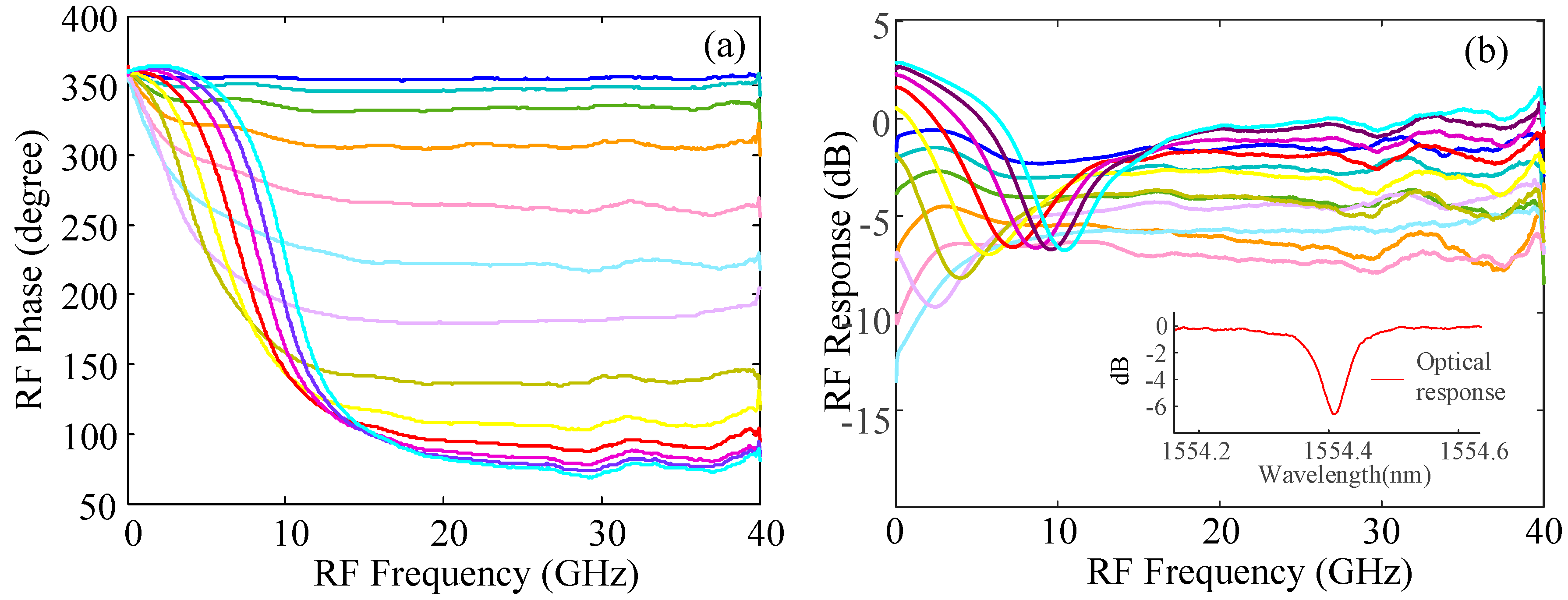
Figure 2.
(a) Schematic of eye-like ring resonator delay line with unbalanced temperature-controlled Mach Zehnder Interferometer (MZI) power splitter. (b) The dependence of the through port group delay τg and optical power transmission |HR|2 on field coupling ratio κ1 or 2 in (b) fast light and (c) slow light regimes.

Figure 3.
(a) Schematics and (b) illustration of the proposed single passband microwave photonic filter (SPMPF).
Figure 3.
(a) Schematics and (b) illustration of the proposed single passband microwave photonic filter (SPMPF).
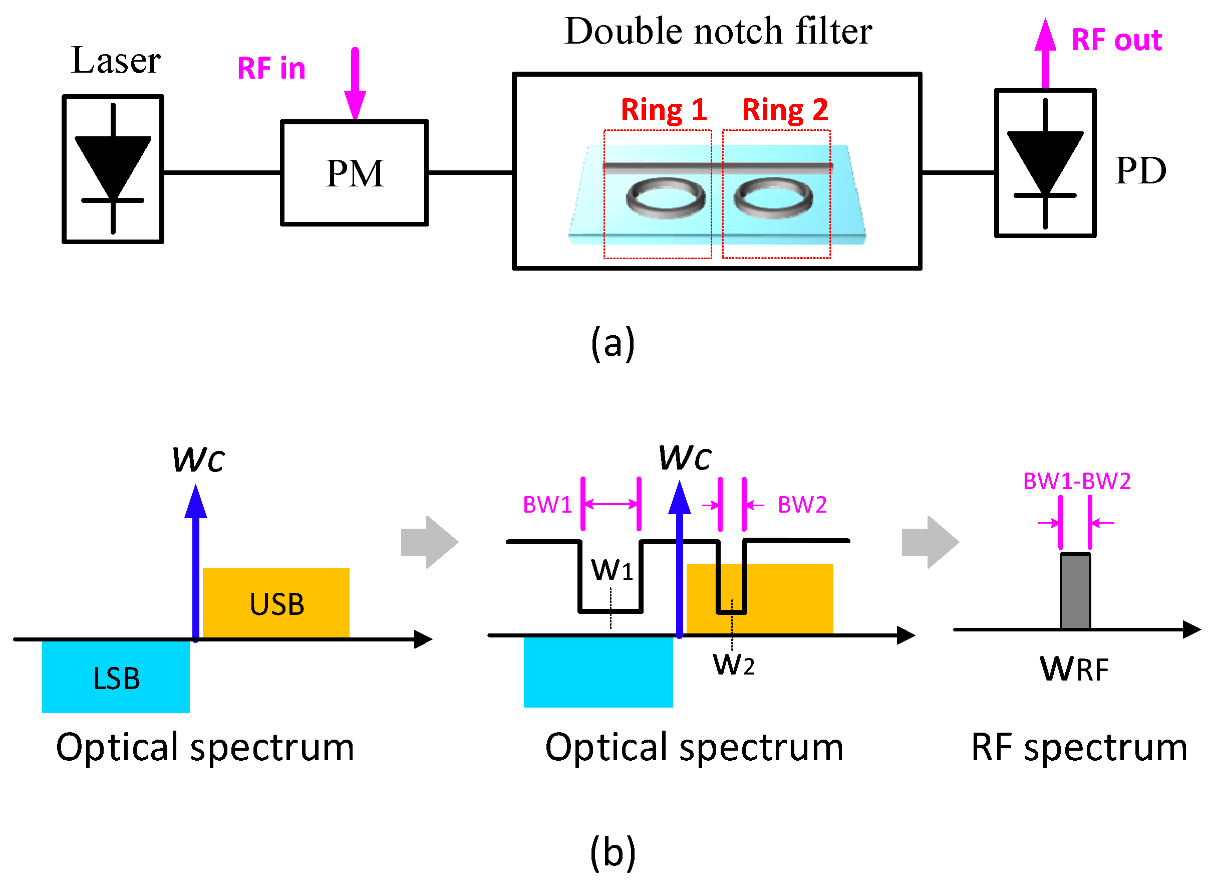
Figure 4.
(a) Schematic diagram of the integrated optoelectronic oscillators (OEO)-based temperature sensor. PM: phase modulator; EDFA: Erbium doped fiber amplifier; EA: electronic amplifier; PC: polarization controller; ESA: electrical spectrum analyser. Experimental results after closing the OEO loop (b) Measured RF response at 24.78 °C. Inset: Zoomed-in response of the RF oscillation mode. (c) Measured RF oscillation frequency shift with temperature variations (d) Measured oscillation frequency shift as a function of the temperature
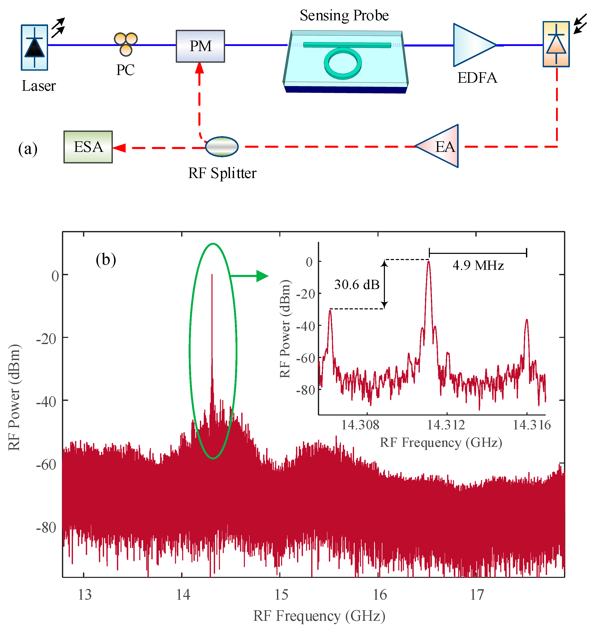
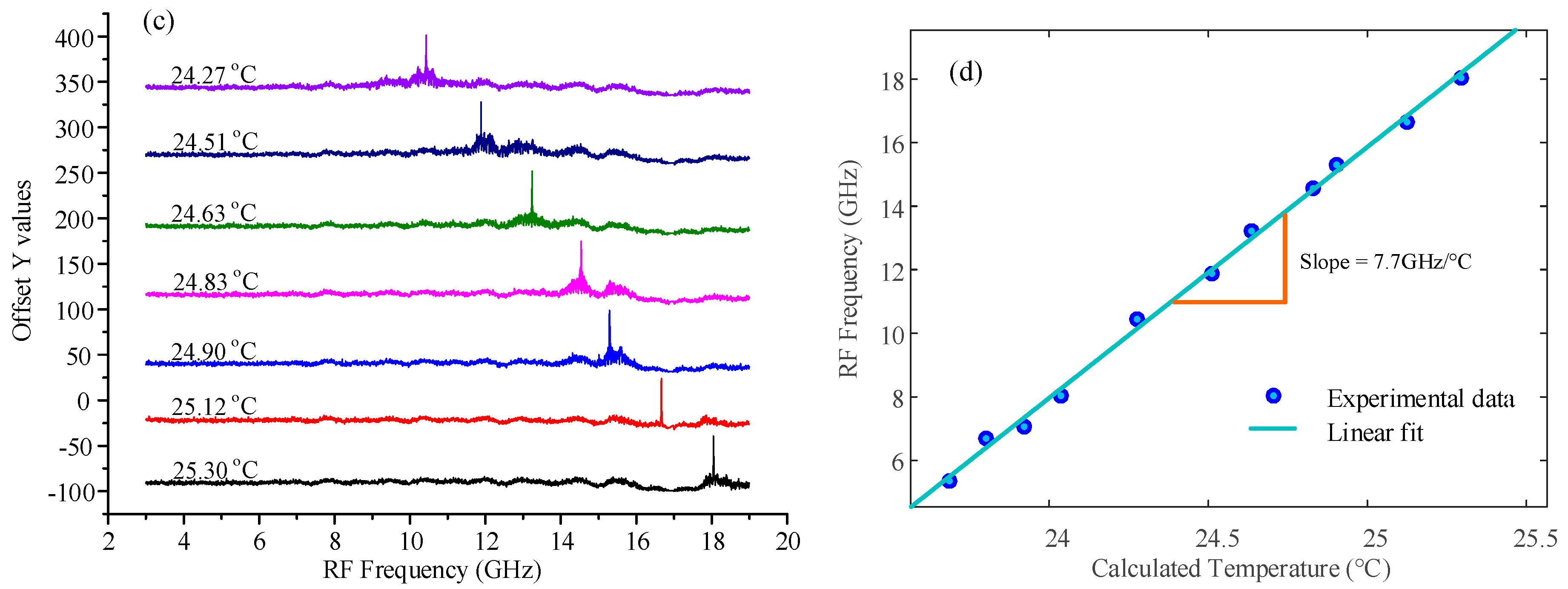
Figure 5.
Schematic diagram of the distributed optical signal processing MWP subsystem with cascaded functionalities.
Figure 5.
Schematic diagram of the distributed optical signal processing MWP subsystem with cascaded functionalities.

© 2017 by the authors. Licensee MDPI, Basel, Switzerland. This article is an open access article distributed under the terms and conditions of the Creative Commons Attribution (CC BY) license (http://creativecommons.org/licenses/by/4.0/).
Share and Cite
MDPI and ACS Style
Yi, X.; Chew, S.X.; Song, S.; Nguyen, L.; Minasian, R. Integrated Microwave Photonics for Wideband Signal Processing. Photonics 2017, 4, 46. https://doi.org/10.3390/photonics4040046
AMA Style
Yi X, Chew SX, Song S, Nguyen L, Minasian R. Integrated Microwave Photonics for Wideband Signal Processing. Photonics. 2017; 4(4):46. https://doi.org/10.3390/photonics4040046
Chicago/Turabian StyleYi, Xiaoke, Suen Xin Chew, Shijie Song, Linh Nguyen, and Robert Minasian. 2017. "Integrated Microwave Photonics for Wideband Signal Processing" Photonics 4, no. 4: 46. https://doi.org/10.3390/photonics4040046
Note that from the first issue of 2016, this journal uses article numbers instead of page numbers. See further details here.