Article

Heat Dissipation Schemes in AlInAs/InGaAs/InP Quantum Cascade Lasers Monitored by CCD Thermoreflectance

1
Institute of Electron Technology, Al. Lotników 32/46, 02-668 Warszawa, Poland
2
Faculty of Microsystem Electronics and Photonics, Wrocław University of Technology, Janiszewskiego 11/17, 50-372 Wrocław, Poland
*
Author to whom correspondence should be addressed.
Photonics 2017, 4(4), 47; https://doi.org/10.3390/photonics4040047
Submission received: 10 November 2017 / Revised: 29 November 2017 / Accepted: 30 November 2017 / Published: 3 December 2017

Abstract

:
In this paper, we report on the experimental investigation of the thermal performance of lattice matched AlInAs/InGaAs/InP quantum cascade lasers. Investigated designs include double trench, single mesa, and buried heterostructures, which were grown by combined Molecular Beam Epitaxy (MBE) and Metal Organic Vapor Phase Epitaxy (MOVPE) techniques. The thermal characteristics of lasers are investigated by Charge-Coupled Device CCD thermoreflectance. This method allows for the fast and accurate registration of high-resolution temperature maps of the whole device. We observe different heat dissipation mechanisms for investigated geometries of Quantum Cascade Lasers (QCLs). From the thermal point of view, the preferred design is the buried heterostructure. The buried heterostructures structure and epi-layer down mounting help dissipate the heat generated from active core of the QCL. The experimental results are in very good agreement with theoretical predictions of heat dissipation in various device constructions.

1. Introduction

Since first demonstration [1] of a Quantum Cascade Lasers (QCLs) over twenty years ago, they have become an important and attractive source of infrared radiation in an extensive wavelength range spanning the mid-infrared and terahertz regions [2,3,4,5]. QCLs have also found an increasing number of military and civilian applications in remote sensing, chemical sensing, and free-space communication systems [6,7].
However, there remains an important issue in the technology of QCLs, which is the capability to extract heat out of the laser active area in order to reduce the increase of the temperature. High temperature not only reduces most performance metrics, but it also decreases device lifetime and impairs its reliability, leading to the degradation of the laser mirror and the destruction of the device. Figure 1 shows an example image of degradation of front facet of QCL taken by optical microscopy and by scanning electron microscopy (SEM). Image shows a blister on the facets of the device, formed during the catastrophic damage of laser in the vicinity of front facet.
Recently, an increased number of degradation observations is reported in the literature [8,9,10]. The problem is undertaken by leading research centers, mostly by theoretical analyses with very few reports concerning experimental works towards the explanation of the observed degradation modes. The experimental techniques applied, like Raman spectroscopy [11] or photoluminescence [12,13], do not allow for the mapping of surface temperature with high spatial resolution.
In order to study and understand problems of thermally induced QCL mirror degradation, an important step is to measure the temperature at small size scales, dictated by small active region dimensions on the order of several square micrometers, with high spatial and temperature resolution. Monitoring of the facet temperature is very useful for the study of the thermal processes and failure mechanisms, and also for the increased reliability and performance of QCLs, as it provides a mode for comparing different packages, geometries, and device designs.
This paper describes the comparison of heat dissipation schemes in lattice matched AlInAs/InGaAs/InP QCL with different ridge geometries and different packages. For this purpose, we have employed an experimental technique that is based on thermoreflectance spectroscopy (TR). Our implementation of the technique is based on Charge-Coupled Device (CCD) camera (CCD TR), which is characterized by high spatial and temperature resolution, and, at the same time, short measurement time [14]. Experimental results are compared to results of numerical heat transfer modeling based on the commercial finite element solver [15].

2. Materials and Methods

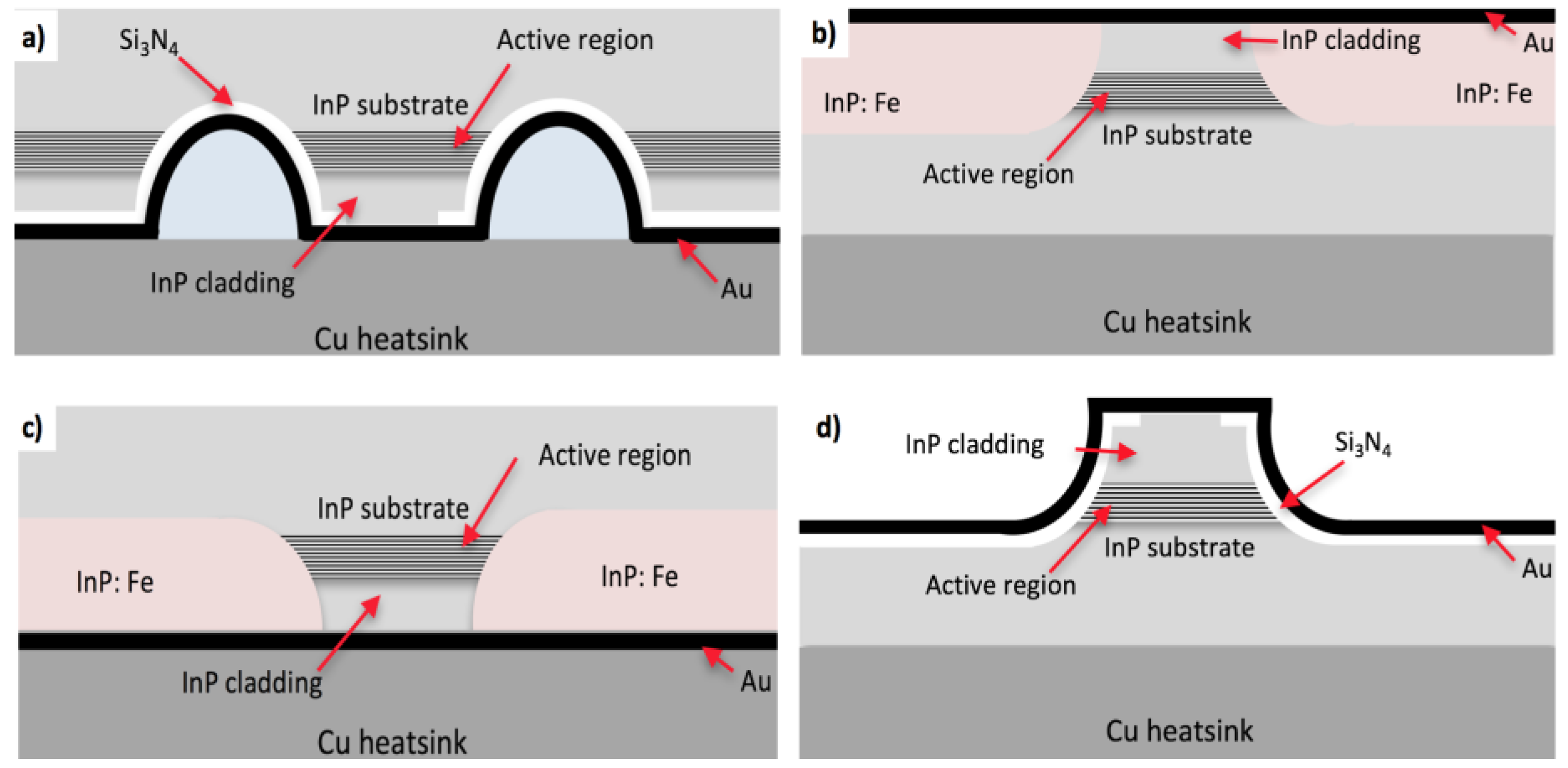
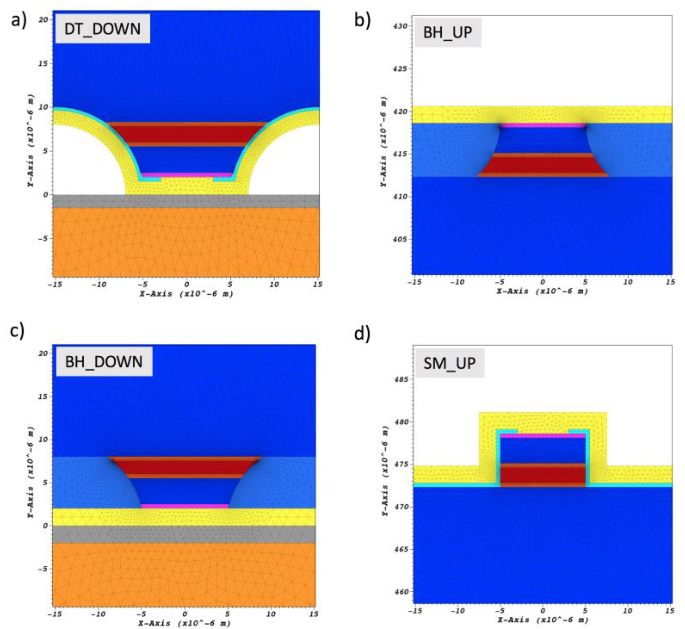
2.1. Investigated Samples

The study of thermal properties was performed for lattice matched AlInAs/InGaAs/InP QCLs grown by hybrid technology MBE (Molecular Beam Epitaxy) + MOVPE(Metal Organic Vapor Phase Epitaxy), designed for emission at about ~9.2 µm. The MOVPE overgrowth was performed in order to form optimum waveguiding layers. Growth of the active region was performed by solid source MBE on Riber Compact 21T reactor. MOVPE overgrowth was performed using AIXTRON 3 × 2” FT LP-MOVPE system with vertical, shower-head reactor. The AlInAs/InGaAs active region of the laser was grown on lightly doped (n = 2 × 1017 cm−3) InP substrate serving as a lower waveguide. The InP top waveguide consisted of 1.5 μm, n = 4 × 1016 cm−3 layer, followed by 1.5 μm, n = 1 × 1017 cm−3 layer. The whole structure was completed by highly doped (n = 8 × 1018 cm−3) contact layer. In this design, the AlInAs MBE grown waveguide (first proposed by Faist et al. [16]) is replaced by InP cladding. This symmetrizes the refractive index profile, enhances the confinement due to higher refractive index contrast, and improves heat extraction, as the thermal conductivity of InP is much better (68 Wm−1 K−1) than for AlInAs (5 Wcm−1 K−1) [17]. The details of the layer structure of the laser are listed in the Table 1.
The 2-inch epitaxial wafer of AlInAs/InGaAs/InP QCL was divided into quarters, subsequently fabricated into four sets of devices that were differing in ridge geometry and assembly type. The types of devices were as follows: the lasers of set A were processed in standard double trench (DT) technology and mounted epi-layer side down, set B was processed into buried heterostructure (BH) and mounted epi-layer side up, set C was processed into buried heterostructure (BH) and mounted epi-layer side down, and set D was processed into single mesa geometry (SM) and mounted epi-layer side up. Schematic drawings of these geometries are shown in Figure 2. In all of the cases, laser chips were indium soldered to the copper heatsink.

2.2. CCD Thermoreflectance Spectroscopy

TR spectroscopy was used in order to gain insight into the thermal properties of investigated QCLs. TR spectroscopy relies on a measurement of the change of reflectance spectrum that is caused by periodic variation of the temperature of the sample [18]. Modulation of temperature is obtained by operating device in a pulsed mode; the device is heating up during the pulse and cools down to heatsink temperature between pulses. The variation of the sample reflectance (∆R) is related to the temperature variation (∆T) through the following relation:
Δ T = ( 1 R R T ) 1 Δ R R C T R Δ R R
Relative change in the optical reflectance per unit temperature change is termed the thermoreflectance coefficient (CTR). The CTR varies strongly with material and the probe beam wavelength, and its typical magnitude ranges from 10−6 to 10−4 for metals and semiconductors.
Thermoreflectance measurements can be realized in two experimental configurations. The CCD TR [14,19], in which a lamp with narrow bandpass filters or a LED illuminator is used to produce the probe light (spectrally narrow) and the whole thermal image is stored in one snapshot by CCD camera. In the other configuration, known as classical or focused laser beam configuration [20,21,22], the appropriate laser line is used as a probe beam for examining the structure. The thermal image is registered by scanning the sample surface point by point. CCD TR was employed for the registration of thermal maps of the front facet of QCLs, as it provides a high speed of registration of the temperature image and sufficient spatial resolution that is required to reveal subtle construction details of the laser. More details concerning the experimental setup and measurement methodology can be found in our previous paper [23]. Thermal management in QCLs was also studied numerically, with a thermal model that was based on the commercial finite element solver [15]. Internal temperature rises, as well as the influence of different mounting options and device geometries on thermal performance of lasers were studied. Figure 3 presents the actual geometry that was used for the simulation process of all tested devices. In this work, we have performed steady state, two-dimensional (2D) simulation of heat transport.

3. Results

In this part, experimental results of the thermal investigation of four sets of lasers differing in ridge geometry and assembly type will be presented.
Set A-DT lasers were fabricated from MBE grown wafers with MOVPE overgrowth of top InP waveguide using standard processing technology, i.e., wet etching and Si3N4 for electrical insulation. The low resistivity, RTA alloyed at 370 °C for 60 s, Ti/Pt/Au ohmic contacts to epi-side, and AuGe/Ni/Au at the substrate side of the device were used. For current injection, windows were opened through the insulator with width 15 μm. The individual cleaved lasers, 2 mm long were soldered epi-side down to Au-plated AlN submount, and then to copper mounts. Set B-BH devices were grown using additional MOVPE regrowth step. The structure was processed to define ridges. In the next step, ridges were protected by Si3N4 dielectric layers [24]. Finally, the wafer was regrown with InP:Fe insulating layer. The last step is to remove the Si3N4 layers and deposit metallic contact layers. The set B lasers were mounted epi-layer side up. Set C devices were grown and processed as BH geometry using the same technology as set B, but contrary to the previous case were mounted epi-side down. The final group of investigated devices (set D) were grown using the same technology like set A devices; i.e., hybrid approach combining MBE grown of AlInAs/InGaAs active region with MOVPE grown InP waveguide layer, and then processed into SM geometry and mounted epi-side up.
Figure 4 shows room temperature (RT), light-current-voltage (LIV) characteristics for all the sets of investigated QCLs. The data were collected in pulsed operation mode using 200 ns current pulses with 5 kHz repetition rate at RT. The inset shows emission spectrum registered at RT and the current density of J = 4.0 kA/cm2. The measurement conditions were chosen to make sure that there is no heating of the devices, so any changes in the observed characteristics are result exclusively from the differences in the device design. The LIV characteristics measured at the 10 μs pulses and 20 kHz repetition rate (supply conditions used for thermoreflectance measurements) are presented in Figure 4. The increase of threshold current density in case of the increased duty cycle is clearly visible. This is a result of increased heating of the devices.
We have performed CCD TR measurements for investigated device groups. In case of TR measurements, an important part of the measurement is the determination of the calibration coefficient CTR. Such calibration was performed for each device. Details on the calibration procedure can be found in [23]. The CTR for InP region is 4 × 10⁻⁵ and for Active Region (AR) layers, an average value of CTR is 5.2 × 10⁻⁵.
Devices were characterized in terms of facet temperatures during different operating conditions (current I = 0.45 A (J = 1.5 kA/cm2) and I = 1.2 A (J = 4.0 kA/cm2). The results that are presented in this work refer to pulse operation with frequency f = 20 kHz and pulse width τ = 10 μs. The bottom side of the laser submount was temperature stabilized at THS = 25 °C using Peltier cell. Figure 5 presents temperature distribution maps on the front facet for all investigated laser designs, recorded for driving current I = 1.2 A (J = 4.0 kA/cm2).
For DT lasers that are mounted epi-layer side down, the maximum temperature increase equals ∆T = 105 K for driving current J = 4.0 kA/cm2, and is localized mainly in the active area. We observe temperature distribution, with heat primarily escaping by upper cladding and through the substrate, with the temperature reaching that of the heat-sink at the distance of approximately 30 μm. For BH lasers, InP:Fe improves device thermal performance allowing for heat to escape from the active region in the plane of the active region layers. Laterally overgrowing ridge waveguide with InP:Fe increases the efficiency of heat removal from the active region. The BH approach combined with epi-layer down mounting allowed for the lowering of the internal temperature of the active area due to the shorter heat transfer path to the heatsink. We observed the reduction of the heat piled-up in the active core region. The maximum ∆T decreases down to 80 K at J = 4.0 kA/cm2. In this configuration, also a substantial amount of heat is removed upward through thick InP substrate with high thermal conductivity. The BH lasers, epi-layer side up bonded do not show such improvement of thermal properties. The temperature increase in the active region reaches ∆T = 140 K for driving current J = 4.0 kA/cm2. Finally, the SM epi-layer up mounted devices definitely show the worst thermal properties when compared to the all of the so far discussed devices. For the SM devices, we observe the temperature of the active region increases by ∆T = 160 K at J = 4.0 kA/cm2.
The horizontal temperature line scans across the laser facet at the center of the active area for all types of investigated lasers are presented in Figure 6. Once again, it can be seen that BH approach combined with epi-layer down mounting shows superior thermal properties. Contrary to all the other cases, we do not observe heat accumulation in the top InP waveguide. The temperature increase at the the interface between laser chip and the heat sink goes to zero. This is not the case of BH epi-layer up mounted laser, where the temperature at the top of the laser chip can be even 60 K higher than the temperature of the heat sink. For SM epi-layer up mounted laser, we observe a similar, although less pronounced, thermal behaviour.

4. Discussion

A summary of all the experimental results and comparison with numerical simulations is given in present section. The thermal properties of different geometry and mounting configuration of lattice matched AlInAs/InGaAs/InP QCLs are discussed. In Figure 7, we present the comparison of vertical line scans that are registered at the same current density Jth = 4.0 kA/cm2 and maximal temperature change as a function of current density for all of the investigated types of QCLs. We observe that maximal temperature increase is in all cases is localized in the active area, and is the highest for group D devices processed into SM geometry and mounted epi-layer up (Figure 7a). The superior temperature properties are exhibited by set C devices, processed as BH and mounted epi-layer side down. The BH epi-layer side down mounted device shows the efficiency of heat removal from the active region two times better than SM epi-layer side up mounted devices for all of the currents (Figure 7b).
Further insight into mechanisms of heat dissipation in different QCL construction is provided by the study of temperature distribution profiles in selected directions. Figure 8 presents enlarged thermoreflectance maps, together with horizontal and vertical line scans, for each of the examined group of lasers.
The maps are recorded at the same experimental conditions; pulse width 10 μs, frequency 20 kHz and driving current density 4.0 kA/cm2. The enlarged temperature distribution maps (20 µm × 10 µm) cover the active area. We clearly see differences in direction and way of heat dissipation from the active area for different ridge configurations. The essential features of heat dissipation can be summarized as follows:
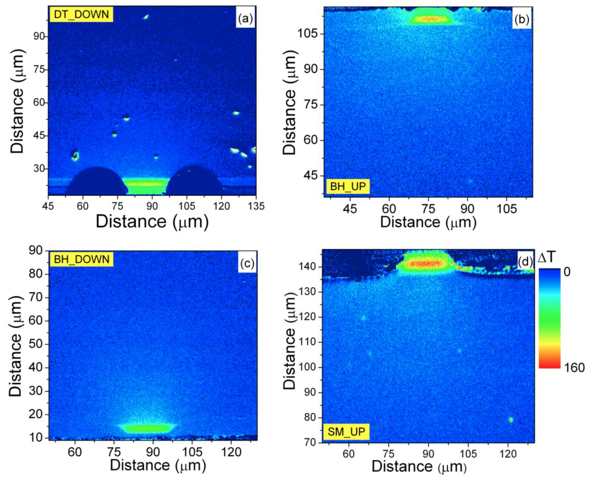
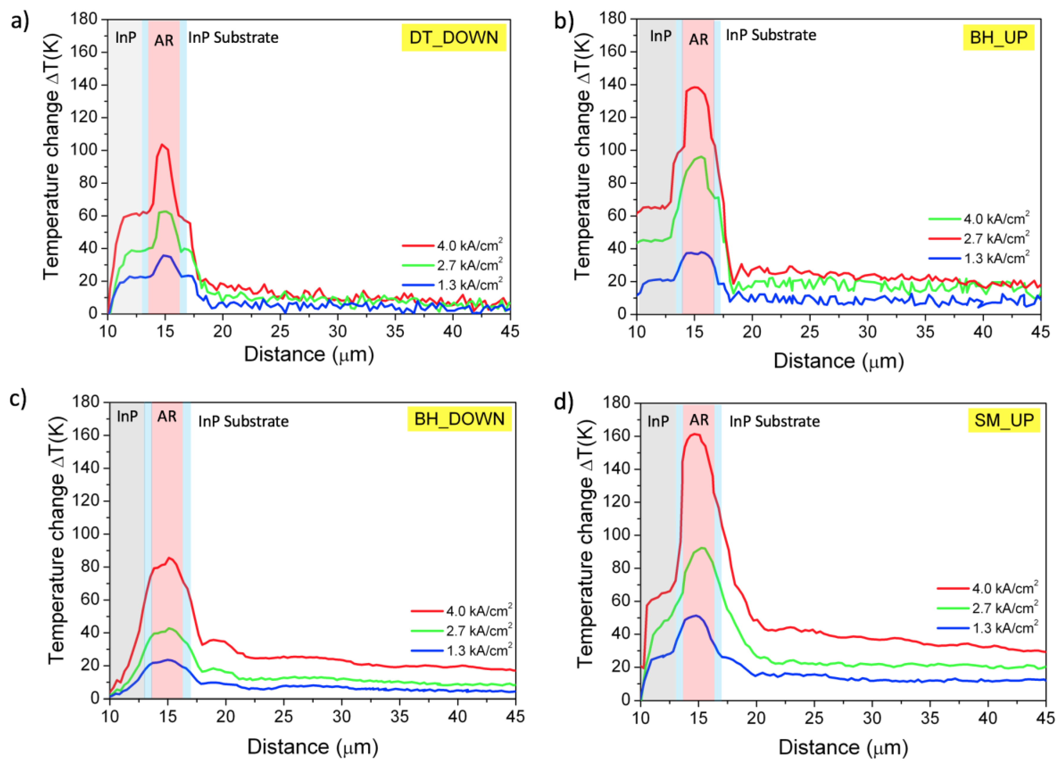
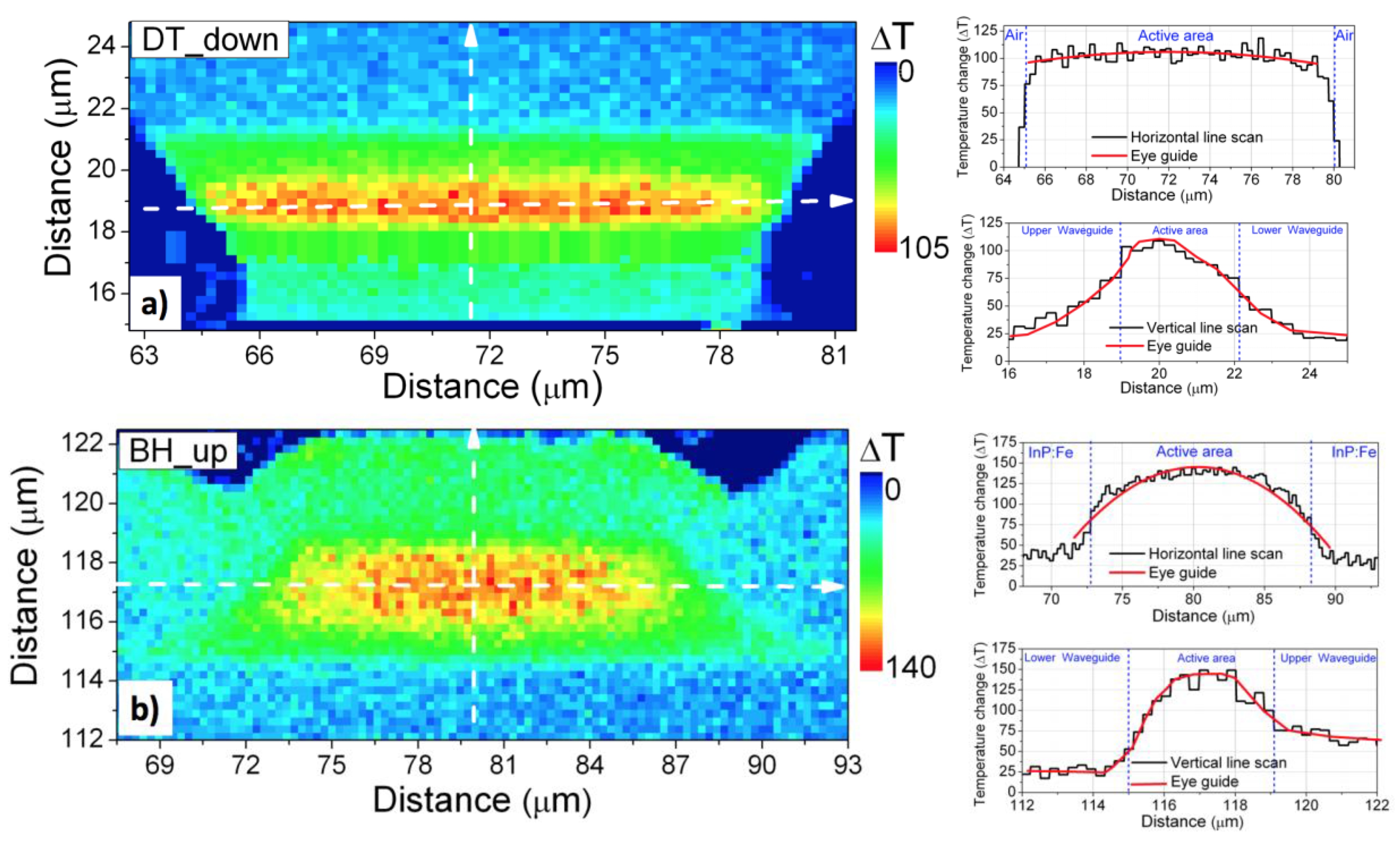
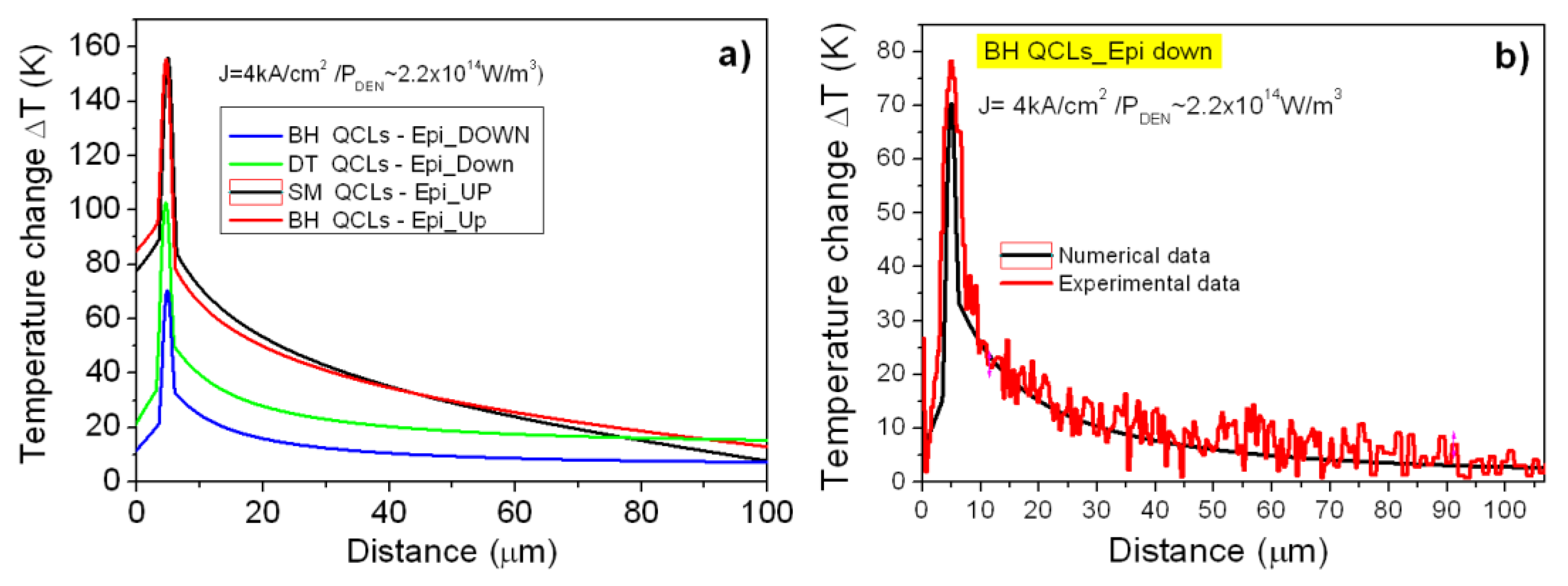
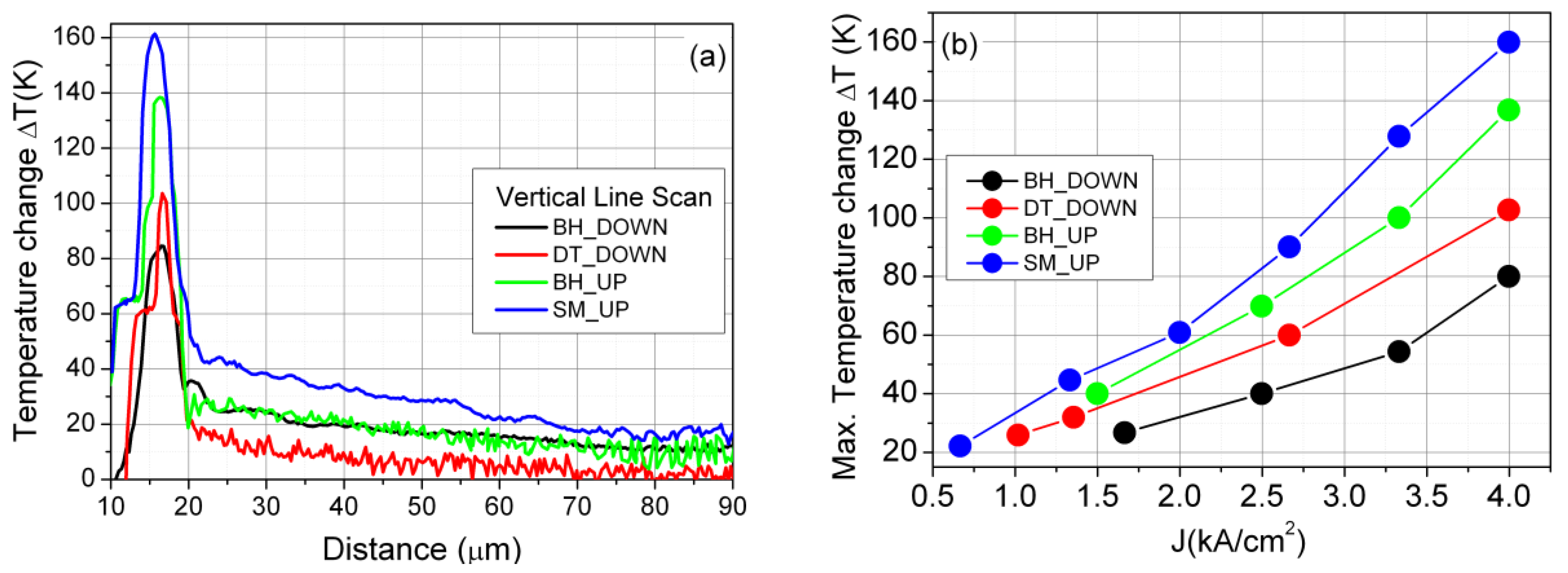
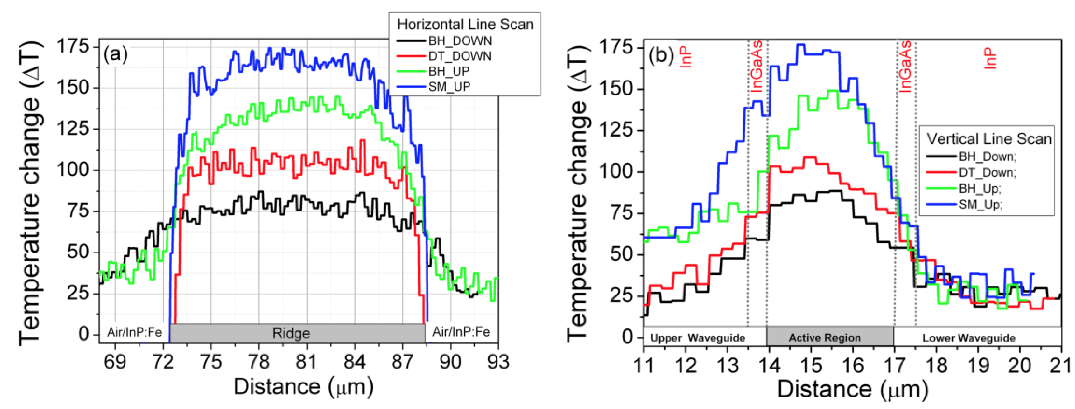
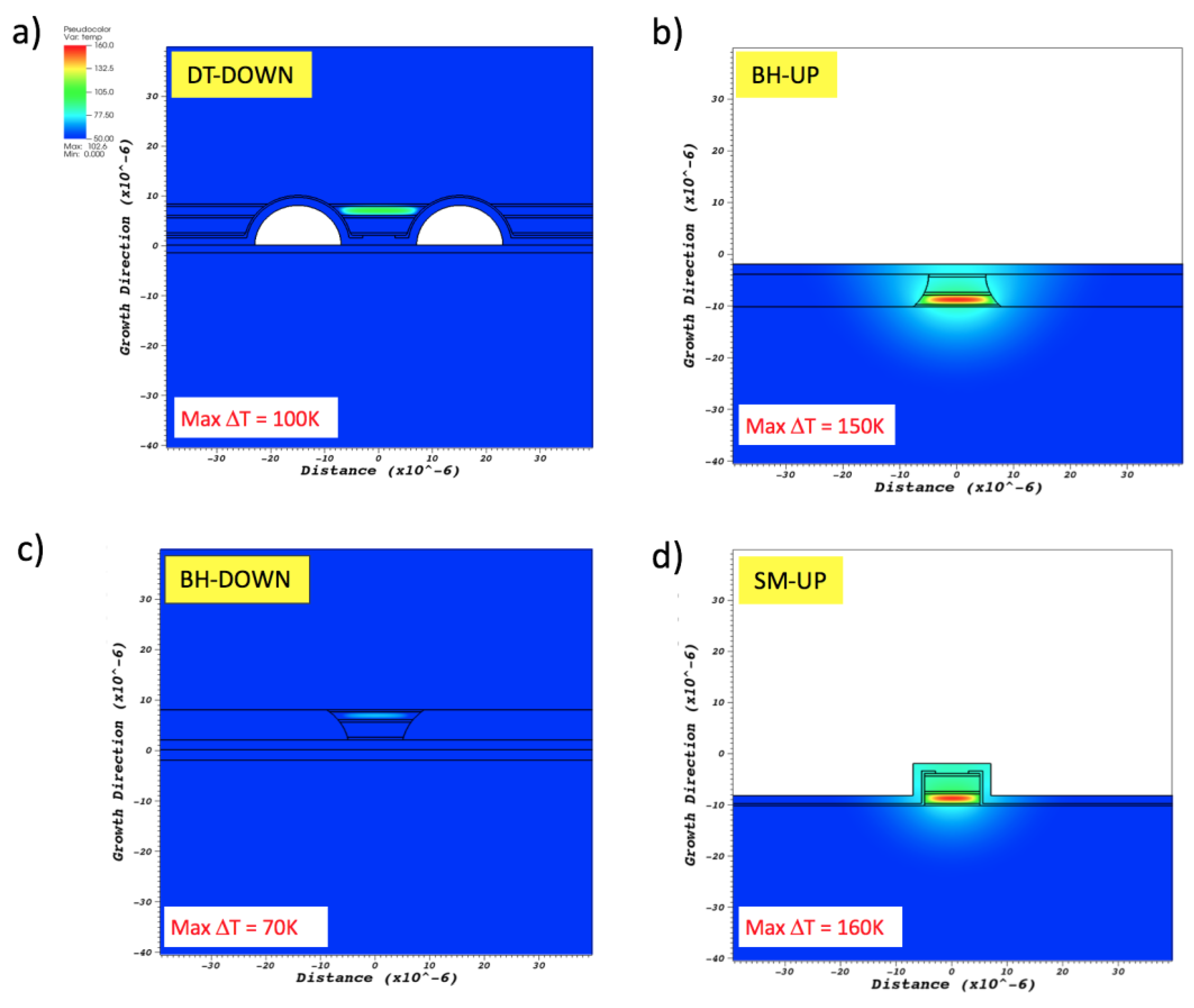
  • For epi-layer down mounted DT (Set A), the horizontal line scan that is taken in the center of the active area, parallel to the epitaxial layers, shows almost uniform heat distribution in the active area. The difference in temperature between the middle and the edges of the active area equals ~8 K, which amounts to 7.6% of the total increase of temperature in the active region. The vertical line scan, taken in the center of the active area perpendicular to the epitaxial layers, shows symmetrical heat dissipation in the direction of upper waveguide/heat sink and lower waveguide/substrate.
  • For epi-layer up mounted BH QCLs (Set B), the horizontal line scan shows non-uniform heat distribution in the active area. The difference in temperature between the middle and the edges of the active area equals ~100 K, which amounts to 71% of the total increase of temperature in the active region. The large gradients of temperature witness the presence of substantial heat fluxes in the lateral direction. The improved lateral heat extraction results from the presence of InP:Fe layers in the direct neighbourhood of the active region and the lack of low thermal conductivity Si3N4 layer. This is the exact opposite situation to DT devices, where ridge sidewalls are dielectrically insulated and the only mechanism of lateral heat extraction is convection. Nevertheless the overall thermal performance of epi-layer up mounted BH QCL is poor. The reason for that is inefficient heat extraction from the upper waveguide, as evidenced by asymmetric vertical temperature scan.
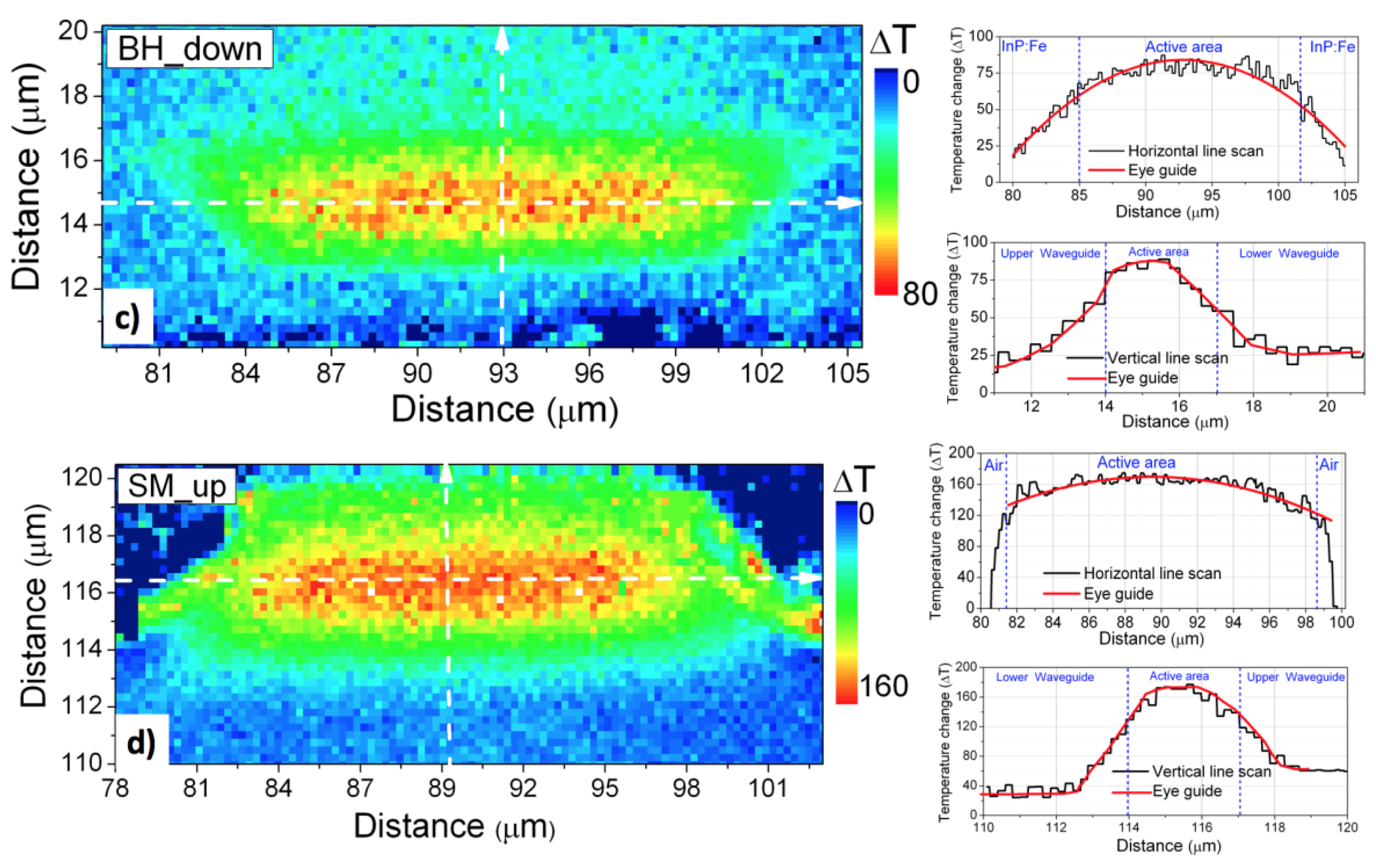
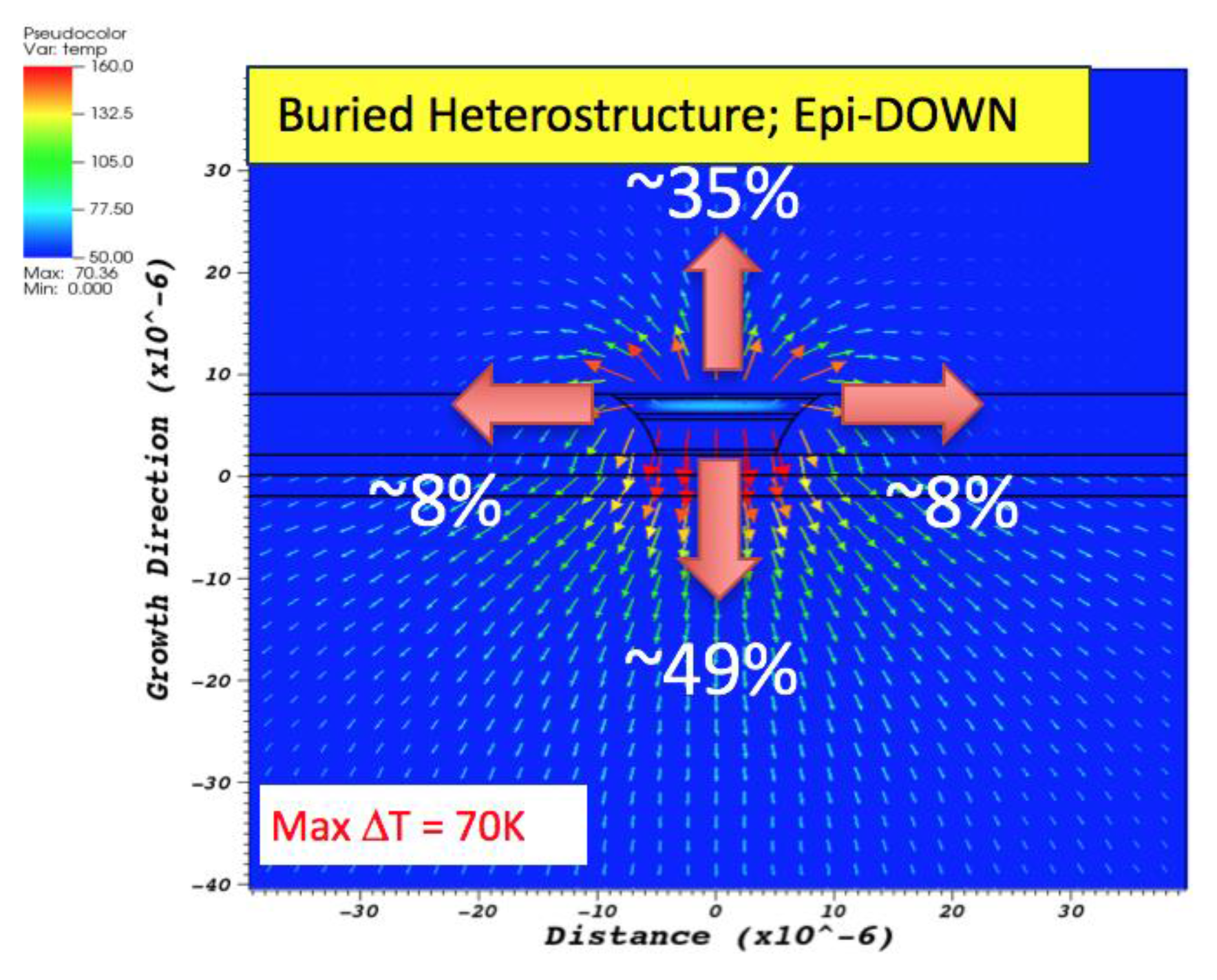
  • For epi-layer down mounted BH QCLs (Set C), the horizontal line scan shows the same behaviour as for epi-layer up mounted BH QCL. The vertical line scan shows efficient heat extraction towards heat-sink located near the active area, which results in the twofold reduction in heat accumulation in the active region. This type of processing and assembling results in best temperature performance from all of the considered designs.
  • For epi-layer up mounted SM QCLs (Set D), almost uniform heat distribution in the active area plane, very poor heat removal from the top and side and the highest temperature increase in the active region is observed.
The horizontal temperature line scans taken parallel to the epitaxial layers, and vertical temperature line scans taken perpendicular to the epitaxial layers recorded at the same current density Jth = 4.0 kA/cm2 for all four groups of investigated QCLs are plotted together in Figure 9. The difference in heat extraction in both directions and superiority of epi-layer side down BH design are clearly visible.
The influence of different mounting options and device geometries on the thermal performance of lasers was also studied numerically with a thermal QCL model based on the commercial finite element solver [14]. Below, we present temperature distribution line scans across the facet, taken at the center of the active area perpendicular to the epitaxial layers for different types of lasers studied (Figure 10a) and a comparison of the calculated profile with experimental line scan for epi-layer side down mounted BH laser (Figure 10b). Calculations have been done for dissipated power density in the active region PDEN = 2.2 × 10¹⁴ W/m3 equivalent to current density Jth = 4.0 kA/cm2.
Figure 11 shows calculated temperature distribution maps for AlInAs/InGaAs/InP QCLs with different mounting options and device designs at constant current density J = 4.0 kA/cm2 (PDEN~2.2 × 10¹⁴ W/m3).
Figure 12 shows heat flux configurations for BH epi-layer down mounted laser. It can be seen, that for this configuration, 49% of total heat escaping from the active region flows through the interface between the top waveguide and the gold layer and down into heat sink. Nevertheless, the amount of heat flowing upward into the substrate due to the high thermal conductivity of InP is still appreciable and amounts to 35%. Both downward and upward fluxes dominate over lateral fluxes, which amount to 8% on each side.
Table 2 presents summary of obtained experimental and numerical results of analysis of thermal properties of studied QCLs that are prepared in different packaging technologies and device designs.
Both experiment and calculations show quite a large difference in temperature increase between epi-layer down and epi-layer up mounted BH lasers. The improvement of thermal properties of epi-layer down lasers has a direct consequence of lowering threshold current density, which is highly desirable property.

5. Conclusions

In this paper, we report on the experimental investigation of the thermal performance of lattice matched AlInAs/InGaAs/InP quantum cascade lasers. Investigated designs included DT, SM, and BH, grown by combined MBE and MOVPE techniques. For BH lasers additional MOVPE overgrowth has been performed. The thermal characteristics of lasers were investigated by CCD thermoreflectance. This method allowed for the registration of high-resolution temperature maps of the whole device facet in several seconds. The CCD-TR proved itself to be a very accurate thermometric technique, opening new possibilities for the optimization of laser's design and degradation studies. We observed different heat dissipation mechanisms for investigated geometries of QCLs. From the thermal point of view, the preferred design is the buried heterostructure. The BH structure and epi-layer side down mounting help dissipate the heat generated from active core of the QCL roughly twice more effective than other designs. The experimental results are in very good agreement with theoretical predictions of heat dissipation in various device constructions.

Acknowledgments

This work was financially supported by National Science Center (NCN) under project no. 2015/17/B/ST7/04015 (OPUS).

Author Contributions

Dorota Pierścińska, Kamil Pierściński and Maciej Bugajski drafted the manuscript. Piotr Gutowski performed MBE growth. Mikołaj Badura, Beata Ściana and Marek Tłaczała were responsible for MOVPE overgrowth. Dorota Pierścińska and Olga Serebrennikova designed and fabricated devices. Dorota Pierścińska, Kamil Pierściński and Grzegorz Sobczak characterized devices, Kamil Pierściński was responsible for numerical simulations. Mikołaj Badura oversaw experiments. All authors discussed results and contributed to formulation of conclusions.

Conflicts of Interest

The authors declare no conflict of interest.

References

  1. Faist, J.; Capasso, F.; Sivco, D.L.; Sirtori, C.; Hutchinson, C.; Cho, A.L. Quantum cascade lasers. Science 1994, 264, 553–556. [Google Scholar] [CrossRef] [PubMed]
  2. Razeghi, M.; Bandyopadhyay, N.; Bai, Y.; Slivken, S. Recent advances in mid infrared (3–5 μm) quantum cascade lasers. Opt. Mater. Express 2013, 3, 1872–1884. [Google Scholar] [CrossRef]
  3. Anders, S.; Schrenk, W.; Gornik, E.; Strasser, G. Room-temperature emission of GaAs/AlGaAs superlattice quantum-cascade lasers at 12.6 μm. Appl. Phys. Lett. 2002, 80, 1864–1866. [Google Scholar] [CrossRef]
  4. Müller, A.; Faist, J. The quantum cascade laser: Ready for take-off. Nat. Photonics 2010, 4, 291. [Google Scholar] [CrossRef]
  5. Faist, J.; Capasso, F.; Sirtori, C.; Sivco, D.; Cho, A. Quantum Cascade Lasers. In Intersubband Transitions in Quantum Wells: Physics and Device Applications, Semiconductor and Semimetals; Academic Press: San Diego, CA, USA, 2000; Volume 66, pp. 1–83. [Google Scholar]
  6. Gmachl, C.; Capasso, F.; Sivco, D.L.; Cho, A.Y. Recent progress in quantum cascade lasers and applications. Rep. Prog. Phys. 2001, 64, 1533–1601. [Google Scholar] [CrossRef]
  7. Pierscinski, K.; Mikołajczyk, J.; Szabra, D.; Pierścińska, D.; Gutowski, P.; Bielecki, Z.; Bugajski, M. Analysis of InP-based QCLs designed for application in optical transmitter of free-space optics. In Proceedings of the SPIE 10437, Advanced Free-Space Optical Communication Techniques and Applications III, 104370A, Warsaw, Poland, 18 October 2017. [Google Scholar]
  8. Xie, F.; Nguyen, H.; Leblanc, H.; Hughes, L.; Wang, J.; Wen, J.; Miller, D.J.; Lascola, K. Long term reliability study and life time model of quantum cascade lasers. Appl. Phys. Lett. 2016, 109, 121111. [Google Scholar] [CrossRef]
  9. Sin, Y.; Lingley, Z.Z.; Brodie, M.; Presser, N.; Moss, S.C.; Kirch, J.; Chang, C.; Boyle, C.; Mawst, L.J.; Botez, D.; et al. Destructive physical analysis of degraded quantum cascade lasers. In Proceedings of the SPIE 9382, Novel In-Plane Semiconductor Lasers XIV, 93821P, San Francisco, CA, USA, 10 March 2015. [Google Scholar]
  10. Zhang, Q.; Liu, F.Q.; Zhang, W.; Lu, Q.; Wang, L.; Li, L.; Wang, Z. Thermal induced facet destructive feature of quantum cascade lasers. Appl. Phys. Lett. 2010, 96, 141117. [Google Scholar] [CrossRef]
  11. Ochalski, T.; Pierścińska, D.; Pierściński, K.; Bugajski, M.; Tomm, J.W.; Grunske, T.; Kozłowska, A. Complementary thermoreflectance and micro-Raman analysis of facet temperatures of diode lasers. Appl. Phys. Lett. 2006, 89, 071104. [Google Scholar] [CrossRef]
  12. Spagnolo, V.; Trocolli, M.; Scamarcio, G.; Gmachl, C.; Capasso, F.; Tredicucci, A.; Sergent, A.M.; Hutchinson, A.L.; Sivco, D.L.; Cho, A.Y. Temperature profile of GaInAs/AlInAs/InP quantum cascade-laser facets measured by microprobe photoluminescence. Appl. Phys. Lett. 2001, 78, 2095–2097. [Google Scholar] [CrossRef]
  13. Fathololoumi, S.; Ban, D.; Luo, H.; Dupont, E.; Laframboise, S.R.; Boucherif, A.; Liu, H.C. Thermal behaviour investigation of terahertz quantum-cascade lasers. IEEE J. Quantum Electron. 2008, 44, 1139–1144. [Google Scholar] [CrossRef]
  14. Farzaneh, M.; Maize, K.; Luerßen, D.; Summers, J.A.; Mayer, P.M.; Raad, P.E.; Pipe, K.P.; Shakouri, A.; Ram, R.J.; Hudgings, J.A. CCD-based thermoreflectance microscopy: Principles and applications. J. Phys. D Appl. Phys. 2009, 42, 143001. [Google Scholar] [CrossRef]
  15. FlexPDE, PDE Solutions, Inc. Available online: http://www.pdesolutions.com/ (accessed on 5 November 2017).
  16. Faist, J.; Capasso, F.; Sirtori, C.; Sivco, D.L.; Baillargeon, J.N.; Hutchinson, A.L.; Sung-Nee, G.C.; Cho, A.Y. High power mid-infrared (λ~5 μm) quantum cascade lasers operating above room temperature. Appl. Phys. Lett. 1996, 68, 3680–3682. [Google Scholar] [CrossRef]
  17. Gresch, T. Gain and Waveguide Engineering in Mid-Infrared Quantum Cascade Lasers. Ph.D. Thesis, Eidgenossische Technische Hochschule ETH Zurich, Rämistrasse, Zürich, 2009. No. 18732. [Google Scholar]
  18. Epperlein, P.W. Micro-temperature measurements on semiconductor laser mirrors by reflectance modulation: A newly developed technique for laser characterization. Jpn. J. Appl. Phys. 1993, 32, 5514–5522. [Google Scholar] [CrossRef]
  19. Tessier, G.; Holé, S.; Fournier, D. Quantitative thermal imaging by synchronous thermoreflectance with optimized illumination wavelengths. Appl. Phys. Lett. 2001, 78, 2267–2269. [Google Scholar] [CrossRef]
  20. Miklos, A.; Lorincz, A. Transient thermoreflectance of thin metal films in the picosecond regime. J. Appl. Phys. 1988, 63, 2391–2395. [Google Scholar] [CrossRef]
  21. Batista, J.A.; Takeuti, D.; Mansanares, A.M.; Silva, E. Contrast and sensitivity enhancement in photothermal reflectance microscopy through the use of specific probing wavelengths: Applications to microelectronics. Anal. Sci. 2001, 17, 73–75. [Google Scholar]
  22. Pierściński, K.; Pierścińska, D.; Iwińska, M.; Kosiel, K.; Szerling, A.; Karbownik, P.; Bugajski, M. Investigation of thermal properties of mid-infrared AlGaAs/GaAs quantum cascade lasers. J. Appl. Phys. 2012, 112, 043112. [Google Scholar] [CrossRef]
  23. Pierścińska, D.; Pierściński, K.; Morawiec, M.; Karbownik, P.; Gutowski, P.; Bugajski, M. CCD thermoreflectance spectroscopy as a tool for thermal characterization of quantum cascade lasers. Semicond. Sci. Technol. 2016, 31, 115006. [Google Scholar] [CrossRef]
  24. Beck, M.; Faist, J.; Oesterle, U.; Ilegems, M.; Gini, E.; Melchior, H. Buried Heterostructure Quantum Cascade Lasers with a Large Optical Cavity Waveguide. IEEE Photonics Technol. Lett. 2000, 12, 1450–1452. [Google Scholar] [CrossRef]
Figure 1. Degradation of front facet of Quantum Cascade Lasers (QCL) evidenced by optical microscopy (a) and by scanning electron microscopy (b). (SEM photo by courtesy of A. Czerwiński, ITE).
Photonics 04 00047 g001
Figure 2. Schematic drawings of lattice matched AlInAs/InGaAs/InP QCL growth by Molecular Beam Epitaxy (MBE) + Metal Organic Vapor Phase Epitaxy (MOVPE) technology, processed in different geometries: (a) double trench (DT) mounted epi-layer side down, (b) buried heterostructure (BH) mounted epi-layer side up, (c) BH mounted epi-layer side down, and (d) single mesa geometry (SM) mounted epi-layer side up.
Photonics 04 00047 g002
Figure 3. Actual input geometries of a QCL used in the two-dimensional (2D) model, (a) DT mounted epi-layer side down, (b) BH mounted epi-layer side up, (c) BH mounted epi-layer side down, and(d) SM mounted epi-layer side up. Calculations were performed on the nonuniform computational mesh. For clarity, mesh density was decreased.
Photonics 04 00047 g003
Figure 4. Light-current-voltage (LIV) characteristics for investigated QCLs: (a) DT epi-layer down mounted, (b) BH epi-layer up mounted, (c) BH epi-layer down mounted, and (d) SM epi-layer up mounted. The data were collected at RT in pulsed operation mode using 200 ns current pulses with 5 kHz repetition rate, as well as 10 μs current pulses with 5 kHz repetition rate. Insets show emission spectra at RT and the current density of J = 4.0 kA/cm2.
Photonics 04 00047 g004
Figure 5. Temperature distribution maps on the front facet of AlInAs/InGaAs/InP QCLs, measured for pulse width 10 μs and frequency 20 kHz for driving currents density 4.0 kA/cm2: (a) DT epi-layer down mounted, (b) BH epi-layer up mounted, (c) BH epi-layer down mounted, and (d) SM epi-layer up mounted.
Photonics 04 00047 g005
Figure 6. Temperature distribution line scans across the laser facet, taken at the center of the active area perpendicular to the epitaxial layers for different values of driving current: (a) DT epi-layer down mounted, (b) BH epi-layer up mounted, (c) BH epi-layer down mounted, and (d) SM epi-layer up mounted.
Photonics 04 00047 g006
Figure 7. (a) Temperature distribution line scans across the laser facet, taken at the center of the active area perpendicular to the epitaxial layers and (b) maximum temperature increases as a function of current density for all investigated types of QCLs.
Photonics 04 00047 g007
Figure 8. Enlarged temperature distribution maps on the front facet and horizontal plus vertical line scans of AlInAs/InGaAs/InP QCLs, for four investigated groups of AlInAs/InGaAs/InP QCLs: (a) epi-layer down mounted DT; (b) epi-layer up mounted BH; (c) epi-layer down mounted BH; and, (d) epi-layer up mounted SM; registered for the same experimental conditions: pulse width 10 us, frequency 20 kHz and driving currents density 4.0 kA/cm2.
Photonics 04 00047 g008aPhotonics 04 00047 g008b
Figure 9. Temperature distribution line scans across the facet taken parallel to the epitaxial layers (a) and vertical temperature line scans taken perpendicular to the epitaxial layers (b) recorded at the same current density Jth = 4.0 kA/cm2.
Photonics 04 00047 g009
Figure 10. The temperature distribution line scans across the facet, taken at the center of the active area perpendicular to the epitaxial layers for different types of lasers studied (a) and comparison of the calculated profile with experimental line scan for epi-layer side down mounted BH laser (b).
Photonics 04 00047 g010
Figure 11. Comparison of calculated temperature distribution maps for AlInAs/InGaAs/InP QCLs: (a) epi-layer down mounted DT; (b) epi-layer up mounted BH; (c) epi-layer down mounted BH; and, (d) epi-layer up mounted SM; calculated for constant current density J = 4.0 kA/cm2 (PDEN~2.2 × 10¹⁴ W/m3).
Photonics 04 00047 g011
Figure 12. Heat flux configuration for BH epi-layer down mounted QCL.
Photonics 04 00047 g012
Table 1. The layer sequence of lattice matched Al0.48In0.52As/In0.53Ga0.47As/InP QCL structure.
ThicknessMaterialDoping
Upper Waveguide
(MOVPE)
500 nmInPn = 8 × 1018 cm−3
1.5 µmInPn = 1 × 1017 cm−3
1.5 µmInPn = 4 × 1016 cm−3
500 nmInGaAsn = 4 × 1016 cm−3
Active Region50 × AlInAs/InGaAs
500 nmInGaAsn = 4 × 1016 cm−3
Lower Waveguide
(MOVPE)
1.5 µmInPn = 4 × 1016 cm−3
1.5 µmInPn = 1 × 1017 cm−3
500 µm
substrate
InPn = 2 × 1017 cm−3
Table 2. The experimental and calculated temperature increases for different types of laser design and mounting options at J = 4.0 kA/cm2 (PDEN~2.2 × 10¹⁴ W/m3).
QCL STRUCTUREMax ∆T(K) ExperimentMax ∆T(K) Simulation
DT_DOWN105 K100 K
BH_DOWN80 K70 K
BH_UP140 K150 K
SM_UP160 K160 K

