1. Introduction
The terahertz spectrum is referred to as the terahertz gap and is defined as the frequency range from 0.1 THz to 10 THz. This frequency region is located between the infrared and microwave regions; it has attracted many researchers and has been studied since the late nineteenth century.
Terahertz technology shows advantages such as characteristic absorption bands for many materials and molecules, high atmospheric absorption, and a nondestructive imaging capability. These advantages have enabled the terahertz ranges to stand out from all other frequency ranges for electromagnetic waves, promising terahertz technologies with strong potential in various fields such as biochemical and medical sensing, information and communication systems, semiconductor and superconductor characterization, non-destructive evaluation, quality control of food and agricultural products, and space and defense industries [
1,
2,
3,
4,
5,
6,
7,
8,
9].
Although the terahertz spectrum promises many significant advantages, obstacles still exist in the evolution of terahertz technology. For instance, current terahertz power generation and receiver technologies are inefficient and impractical. These barriers hamper utilization of the terahertz region compared to neighboring bands because of well-developed optical engineering of low-frequency infrared detectors and already mature technologies for the highest frequencies of the radio spectrum in the microwave region. One of the development limitations is that the frequencies of terahertz waves are too high for current high-frequency electronics. General detectors for high-frequency electronics are mostly based on various high-speed transistors and complicated oscillating circuits, which are limited in operation to approximately hundreds of GHz. Another limitation is that the photon energy of a terahertz wave is much lower than that of visible light, with devices based on traditional optoelectronic materials being extendable only to tens of THz [
10,
11].
Following the development of higher-power sources and nanotechnology for sensitive detectors, terahertz technology has been pushed to the forefront. Numerous breakthroughs have greatly improved the performance of terahertz systems. Details of historical achievements and the fundamental principles of terahertz research can be found in several reviews and books [
8,
9]. The unique advantages and expected applications of the terahertz spectrum have motivated the fabrication of terahertz detectors based on various technologies. Existing technologies include bolometers, thermoelectric sensors, Schottky barrier diodes, quantum effect sensors, and nanowire photoconductive detectors [
12,
13,
14]. However, these techniques have shortcomings, including high cost and complexity, low detection rate, and lack of sensitivity, which affect their usefulness in practical applications. Thermal sensing elements that detect terahertz radiation as heat are either very slow in modulation frequency (10
2~10
3 Hz) or require a harsh operating environment such as deep cryogenic cooling to ~4 K for superconducting hot-electron bolometers [
15]. The terahertz time domain spectroscopy (THz-TDS) system is based on photoconductive detection and electro-optical detection, which works through detection of a terahertz light-induced change in the refractive index of the electro-optical materials. The THz power detected in the THz-TDS is about 1 μW, limiting application in real sample spectroscopy and imaging [
16,
17]. Moreover, data can only be acquired one pixel at a time, which limits the data acquisition rate and largely slows the imaging time. Therefore, the development of technologies for high sensitivity, high responsivity, and low noise equivalent power (NEP) terahertz detectors is strongly demanded for various promising applications. Recently, nanomaterials, together with nanotechnology, have come to challenge many of these requirements and have been widely employed in the design and fabrication of terahertz detectors [
18,
19].
Recently, complementary metal oxide semiconductor (CMOS) and the field-effect transistor (FET) [
20] have been actively studied as terahertz detectors. The detection mechanism for such devices is based on the excitation of an electromagnetic field in the transistor channel [
21]. The operating conditions include the following: a plasma damping rate lower than the inverse of the plasmon transit time in the transistor channel, together with a plasma damping rate lower than the frequency of the incident terahertz signal [
22]. When the impinging electromagnetic radiation contains frequencies higher than 1 THz, these conditions result in a mobility value greater than 104 cm
2/(V·s) for the electrons in the transistor channel. However, when the plasma oscillations are over damped, the detector can function with a broadband detection mechanism. In this situation, the electromagnetic radiation induces an oscillating variation in the FET gate voltage. The gate voltage then biases the channel, modulating the carrier density and the drift velocity, thereby affecting the electron dynamics. Thus, the incident signal can be detected as a DC voltage across the channel under open-circuit conditions. This detection mechanism offers advantages such as sensitive detection and fast response times. This device structure is also convenient for application to large arrays. For example, CMOS and 2D FETs utilizing these schemes have been demonstrated to be functional at high frequencies [
23]. FETs based on nanowires (NWs) as the channel have shown promise for room-temperature, high-sensitivity terahertz detection [
18,
19]. In such devices, the impinging signal is collected by a resonant or a broadband antenna and then fed in to the source and gate terminals.
Table 1 lists the responsivity and NEP from recent studies of NW-based FETs that operate in the terahertz spectral region [
24,
25,
26].
In this paper, we present our NW-based FET terahertz detector. We use Ge-core/amorphous-Si (a-Si)-shell NWs as the active material for the FET detector and employ a bow-tie antenna as the metallic planar antenna for radiation coupling. The Ge-core/a-Si-shell NWs exhibits a much higher field-effect hole mobility compared to the Ge NWs without a-Si-shell, which may lead to a better performance of the device. Electronic characteristics and photoresponse measurements are also carried out in this work. High responsivity with low NEP was demonstrated, which is superior to the results of related studies.
2. Materials and Methods
We have implemented a FET based on Ge-core/a-Si-shell NWs. The hole mobility for Ge is higher than those of Si and III-V semiconductors. Ge is suitable for use as the channel material for high-speed
p-channel FETs [
27]. However, the pure Ge material is easily oxidized. The native oxide of Ge is unstable and soluble in water, making preservation of the Ge NW difficult, which in turn affects the durability of a Ge NW-based device. Therefore, additional artificial surface passivation of Ge NWs is required. Organic layers such as alkanethiols [
28], aqueous halide solutions [
29], and dielectric layers such as aluminum oxide (Al
2O
3) and hafnium(IV) oxide (HfO
2) [
30] can be used to passivate the Ge NW surface. The current method for surface passivation includes use of an a-Si shell deposited by chemical vapor deposition (CVD).
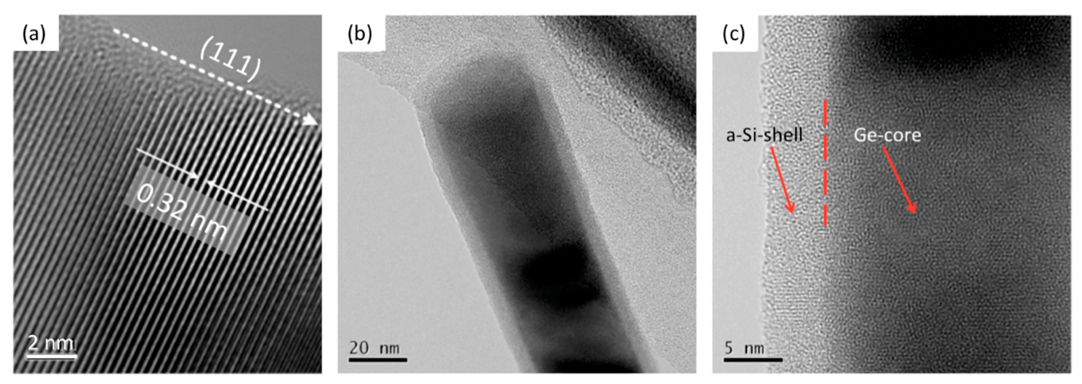
Figure 1 shows a Ge-core/a-Si-shell NW fabricated using CVD, which is used for device fabrication in this work. Our Ge NW cores were grown epitaxially on Ge (111) substrate. High-resolution TEM shows that an individual Ge NW core is a single crystal with a diamond structure and a preferred growth along the <111> direction. The lattice fringe spacing is measured to be ~0.32 nm. The defect density of the germanium core was around 0.2/μm. The amorphous silicon shell was deposited conformally along the observed length. The average diameter of the germanium nanowire core was ~28 nm, the amorphous silicon shell thickness was ~5 nm, and the average of the nanowire length was ~1.2 μm. We selected those nanowires with thinner diameter and longer length for further device fabrication. The field-effect hole mobility of Ge-core/Si-shell NWs used in this work is 664 cm
2/Vs, measured at |
Vsd| = 0.1 V. Compared to the typical field-effect hole mobility in Ge NWs (without an a-Si-shell) of 213 cm
2/Vs [
27], the Ge-core/Si-shell NWs promises a better performance.
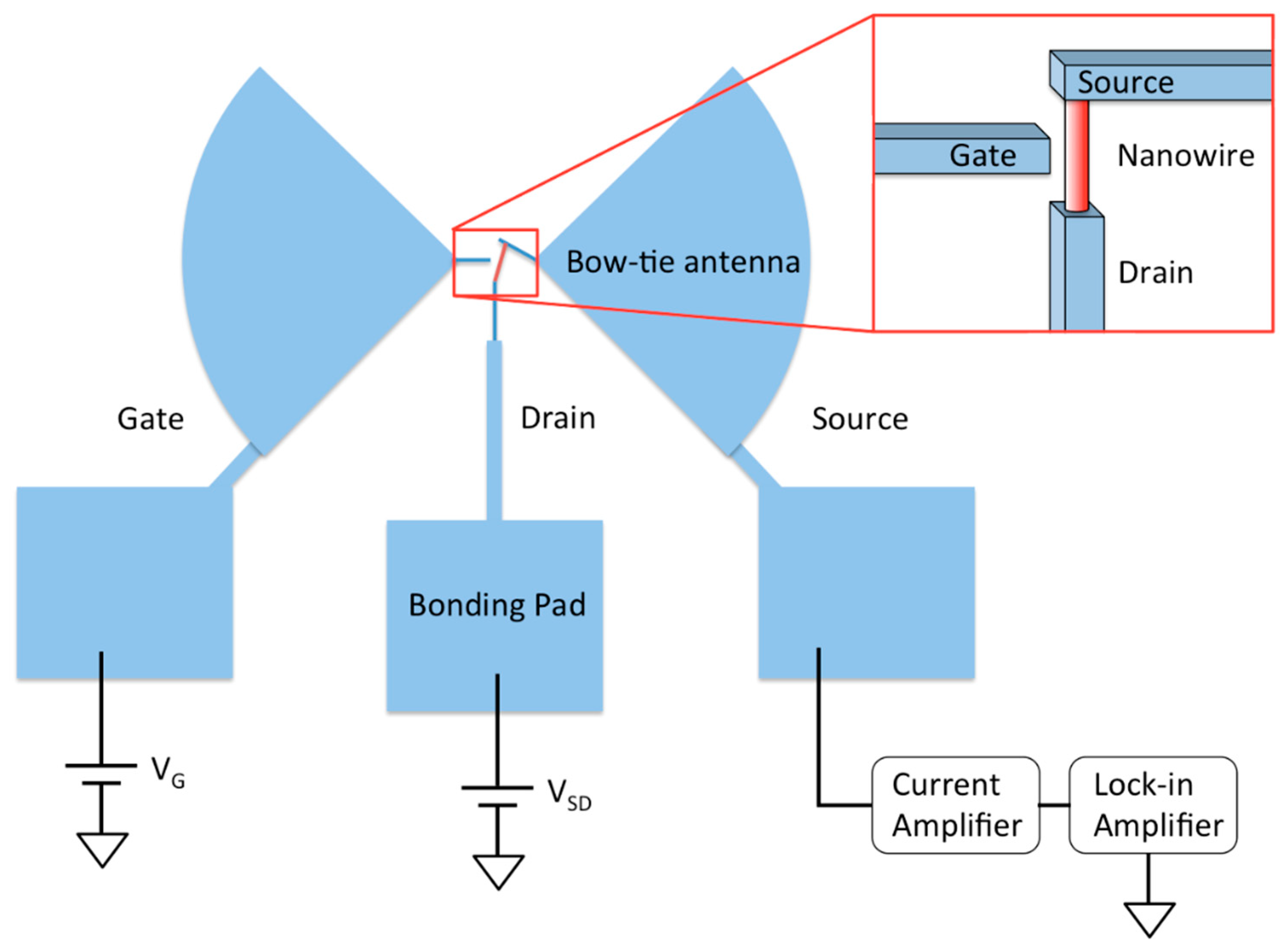
A bow-tie antenna was chosen for coupling with the Ge-core-/a-Si-shell NW. The bow-tie antenna is a common antenna that has been frequently used for NW-based terahertz detectors. It comprises two axisymmetric-placed sectors. The bow-tie antenna is a wide-band antenna, but its frequency range and bandwidth are determined by the radius
r of the sectors. The relationship between
r and
f is given by:
c is the speed of light, and
f is the designed frequency of the antenna.
In this study, we used terahertz gas lasers pumped by CO
2 infrared lasers as the terahertz source, whose effective frequency was 1.63 THz. In this case, we designed the radius of our bow-tie antenna to be 200 μm. A side-gate geometry was used for the device structure. The designed distance between the gate and the nanowire was 200 nm. The source and gate electrodes were connected to the two lobes of the bow-tie antenna, respectively, whereas the drain electrode was connected directly to the bonding pad. The three bonding pads were connected to a power source, a current amplifier, and a lock-in amplifier, as depicted in
Figure 2. In the nanowire-based field effect transistors, the conductivity of the nanowire can be controlled through an external field generated by a gate electrode. The two halves of the bow-tie antenna connected to the gate and source electrodes create an inherent asymmetry between the source and drain. An
ac potential is induced by the incoming radiation between the gate and source electrodes. The modulation of the carrier density of the nanowire and their drift velocity results in the rectification of the
ac potential, which in turn leads to a
dc photoresponse between source and drain.
The device was fabricated according to the following procedure. A Si wafer was cut into 2 cm
× 2 cm squares. The cleaned Si substrate was then placed into an oxidation oven for formation of the SiO
2 layer. In this device, the thickness of the SiO
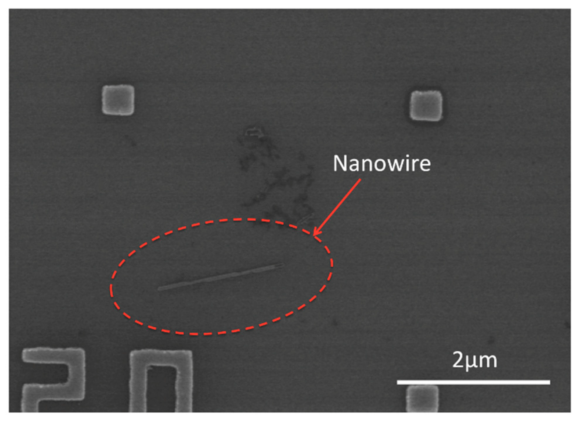
2 layer was designed to be 100 nm. The Ge-core/a-Si-shell NWs were initially grown onto a Ge wafer. To remove the NWs from the substrate, we submerged the wafer into IPA and then ultrasonically agitated it. The NWs were then suspended inside the IPA liquid. Next, we used a dropper to drop cast the NW liquid onto our substrate. During drop casting, frequent checking under a microscope is recommended to ensure that an appropriate number of NWs are on the substrate. The substrate was then transferred to a scanning electron microscope to locate the NWs and record micrographs.
Figure 3 shows a micrograph of a NW lying next to an address mark.
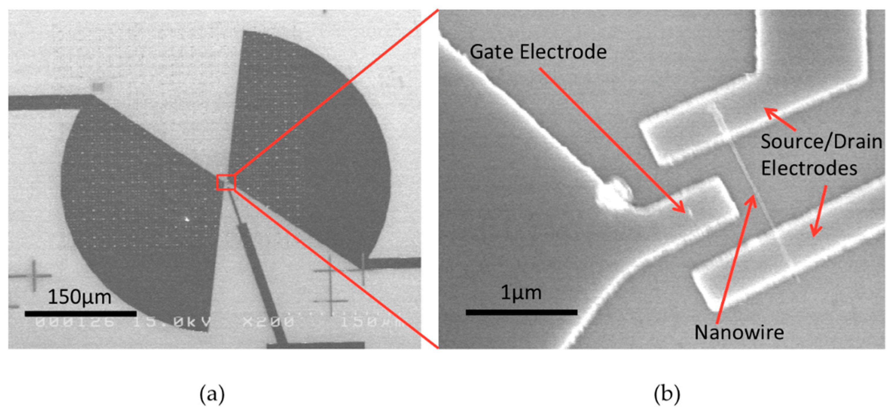
To ensure a good ohmic contact between the source/drain electrodes and the NW, the oxidation layer on the surface of the NW should be removed. The sample is submerged in BHF for 5 s and rinsed in water before being placed into an EBE for metal deposition. Previous experiments have shown that Ni, in comparison with other transition metals, can form a better alloy with the core-shell NWs, which is expected to lead to a better ohmic contact. Therefore, Ni/Au was used as the electrode material as well as contact material for future bonding. In our experiments, the thickness for the deposited Ni was 50 nm and the thickness for Au deposition was 70 nm. After EBE deposition, the substrate was submerged in acetone for lift-off, rinsed in IPA and water, and then prepared for measurement.
Figure 4 presents SEM micrographs of the fabricated device.
3. Measurement Results and Discussion
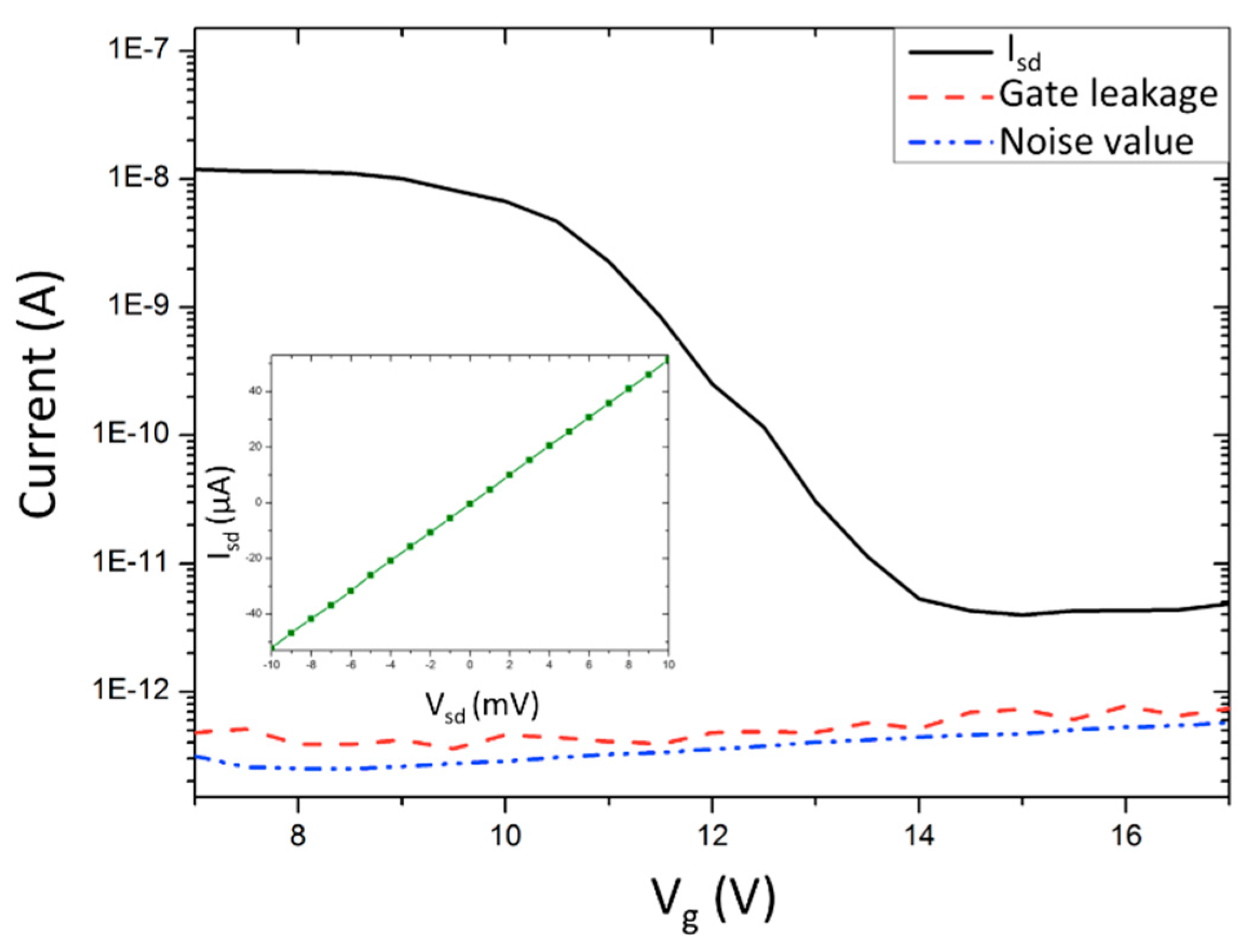
The electronic characteristics of the fabricated devices were measured using a probe station. The results show ohmic contact between the source/drain electrodes and the NW, along with good gate modulation via the side-gate, as shown in
Figure 5. The source-drain current was reduced from 10
−8 A to 10
−12 A when the gate voltage was increased from 10 V to 14 V. The gate leakage and noise value during the measurements were both 10
−13 A, which indicates a good measurement environment with negligible noise. This gate modulation indicates the potential for terahertz detection starting at a gate voltage of 10 V.
The devices were subsequently cut and bonded to chip carriers using an ultrasonic bonding machine. The bonding wire was Al. The bonded chips were transferred to the cryogenic vacuum chamber for measurement of their terahertz response. The pressure inside the chamber was maintained at less than 10
−5 Pa, and the temperature inside the chamber was fixed at 4 K. We used a terahertz gas laser pumped by CO
2 infrared lasers as the terahertz source, with the frequency set to approximately 1.63 THz. The terahertz irradiation was guided through an optical fiber and then transmitted through the transparent aperture into the cryogenic vacuum chamber. The intensity was mechanically chopped, and the induced
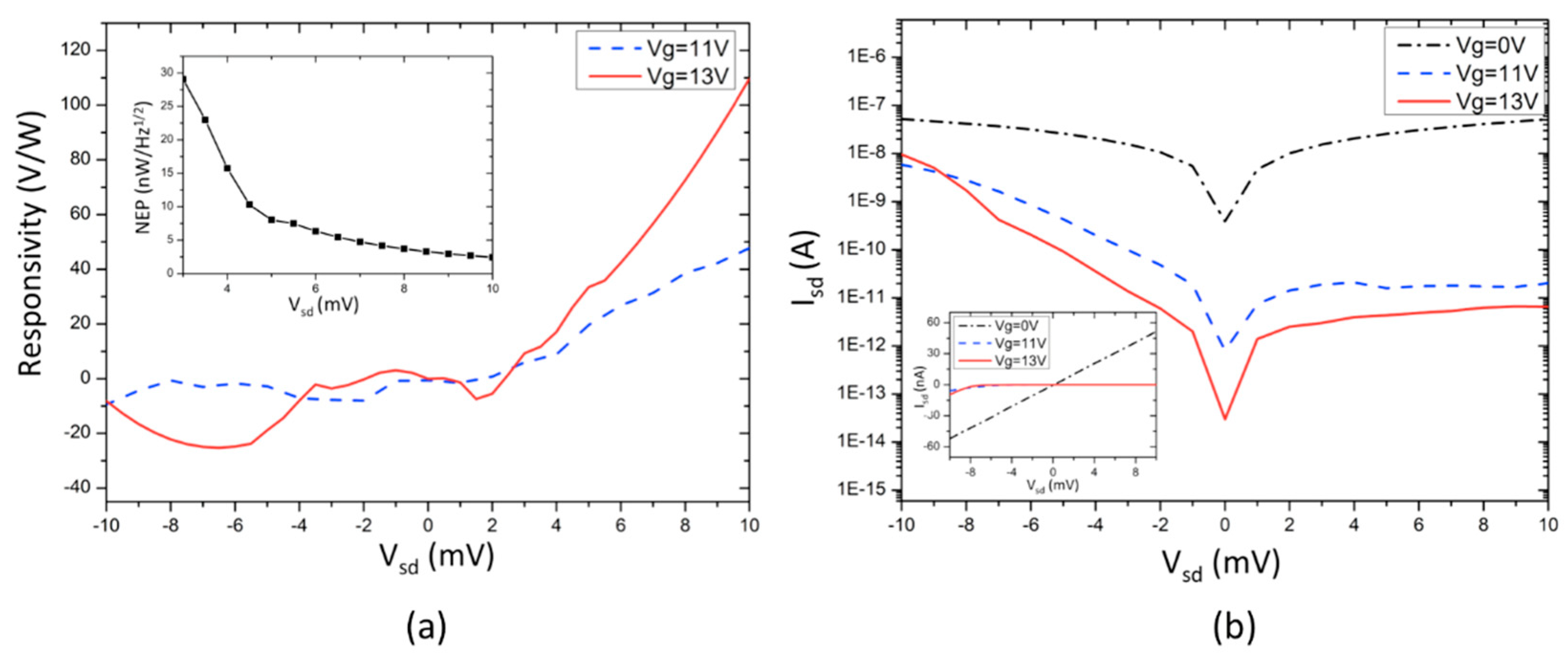
dc photo response was read out at the source electrode by a lock-in amplifier. Upon application of the terahertz signal, a terahertz response was measured as a function of drain voltage; the results are shown in
Figure 6a. The drain voltage was swept from −10 mV to 10 mV with the gate voltage fixed at 11 V and 13 V respectively.
The
I-V characteristic of the NW-based FET (
Figure 6b) was asymmetric when the gate voltage of 11 V and 13 V were applied to the device, which leads to the asymmetric THz photoresponse of the device with respect to the source-drain voltage. Moreover, the measurement results exhibit higher responsivity under higher gate voltage (13 V) when the source-drain current
Isd is nearly vanishing. Such a behavior can be explained using a simple diffusive model: [
31,
32]
where
σ is the conductivity of the FET, Δ
u is the induced dc photoresponse. The formula indicates that the photoresponse is proportional to the derivative of the conductivity as a function of gate voltage, and inversely proportional to the conductivity of the FET. Considering that the value of
dσ/dVg is similar for
Vg = 11 V and
Vg = 13 V, the dramatical decrease of FET conductivity
σ as the gate voltage change from 11 V to 13 V results in an increase of the responsivity. The calculated ratio between the photoresponse for
Vg = 13 V and
Vg = 11 V is:
which is similar to our experimental value:
Additionally, the data shows a larger photoresponse at higher drain voltages, confirming the photovoltage effect of the measurement results. When gate voltage of 13 V is applied, the photocurrent in the NW-based FET reached 56.7 nA upon terahertz irradiation at 1.63 THz at a drain voltage of 10 mV. The power of the irradiated CW THz beam was 0.5 mW, measured at the output of the optic fiber. Considering the diameter of THz spot size was 0.9 mm while the diameter of our bow-tie antenna was 0.4 mm, we estimated the effective power illuminated into the antenna area was 0.1 mW. This leads to a responsivity of approximately 109.6 V/W. The NEP is estimated from the ratio
N/Rv [
25,
33].
Rv is the THz-detected voltage signal, divided by the effective THz power illuminated onto the antenna of the detector. The Johnson-Nyquist noise is expressed as
N = √(4
kBRnwT), which gives 2.69 × 10
−7 V/√Hz for our device. Here
kB is the Boltzmann constant,
Rnw is the resistance of the nanowire, and
T is the measurement temperature. The shot noise is expressed as
N = √(2
eidc), which gives 3.28 × 10
−16 A/√Hz (1.05 × 10
−8 V/√Hz) for our device. Here
e is the elementary charge, and
idc is the average
dc current. The Johnson-Nyquist noise is thus the main source of noise in our measurement. Based on this, we extracted the NEP of the Ge-core/a-Si-shell NW-based FET terahertz detector, as shown in the inset in
Figure 6. A steady NEP appeared when the source-drain voltage was greater than 4 mV. A minimum NEP value of 6.29 × 10
−10 W/Hz
1/2 was achieved at
Vg = 11 V by our fabricated Ge-core/a-Si-shell NW-based THz detector. If the coupling efficiency of the bow-tie shaped antenna is roughly 80% [
34], the intrinsic NEP value is estimated to be 5.03 × 10
−10 W/Hz
1/2.
The improved performance of our Ge-core/a-Si-shell NW-based FET detector is mainly due to high field-effect hole mobility of the Ge-core NW protected by the surrounding a-Si-shell. We selected the NWs with thinner diameter to ensure higher carrier density. The well matching of impedance between the NW-based FET and the bow-tie antenna also led to a better performance. Compared with other recent related studies [
20,
21,
22], the detectivity of our Ge-core/a-Si-shell NW-based FET terahertz detector is superior, along with a smaller NEP. These features indicate that the Ge-core/a-Si-shell NWs show promise as a valid alternative to conventional InAs materials for terahertz detection, with increased sensitivity and a lower NEP. The current distance between the gate and the nanowire was 200 nm. The reduction in this distance will result in the responsivity enhancement. However, the current side-gated model has limitations during fabrication, and it is difficult to achieve a shorter gate-nanowire distance. Top-gated or back-gated model is a possible method to further reduce the gate-nanowire distance and improve the responsivity.


