Fano Resonance Enhanced Surface Plasmon Resonance Sensors Operating in Near-Infrared


1
School of Mechanical Engineering and Electronic Information, China University of Geosciences (Wuhan), Wuhan 430074, China
2
XLIM Research Institute, UMR 7252 CNRS/University of Limoges, 123, Avenue Albert Thomas, 87060 Limoges CEDEX, France
3
School of Electrical and Electronic Engineering, Nanyang Technological University, Singapore 639798, Singapore
*
Author to whom correspondence should be addressed.
†
These authors contributed equally to this work.
Photonics 2018, 5(3), 23; https://doi.org/10.3390/photonics5030023
Submission received: 24 July 2018
/
Revised: 4 August 2018
/
Accepted: 8 August 2018
/
Published: 10 August 2018
(This article belongs to the Special Issue Nonlinear Dielectric Photonics and Metasurfaces)
Abstract
:In the phase-sensitivity-based surface plasmon resonance (SPR) sensing scheme, the highest phase jump usually happens at the darkness or quasi-darkness reflection point, which results in low power for detection. To overcome such a limitation, in this paper, a waveguide-coupled SPR configuration is proposed to work at near-infrared. The coupling between surface plasmon polariton (SPP) mode and photonic waveguide (PWG) mode results in electromagnetically induced transparency (EIT) and asymmetric Fano resonance (FR). Near the resonance, the differential phase between p-polarized and s-polarized incident waves experience drastic variation upon change of the surrounding refractive index. More importantly, since the FR occurs at the resonance slope of SPP mode, the corresponding phase change is accompanied with relatively high reflectivity, which is essential for signal-to-noise ratio (SNR) enhancement and power consumption reduction. Phase sensitivity up to 106 deg/RIU order with a minimum SPR reflectivity higher than 20% is achieved. The proposed scheme provides an alternative approach for high-performance sensing applications using FR.
1. Introduction
Surface plasmon resonance (SPR)-based sensors—characterized by their advantages of label-free, high sensitivity, and low limit of detection for the inspection of liquids and gases—are regarded as a powerful sensing tool in chemistry and biology [1]. However, it is worth noting that for applications of low-molecular-weight (a few hundreds of Daltons) detections including early diagnosis of diseases and pharmacology, the plasmonic technologies still need further improvement [2,3]. Wavelength and angular interrogation are common approaches to implement SPR sensors. However, wavelength/angular interrogation requires high precision instruments to track the variation of the environmental parameters, which is not cost-effective. Intensity interrogation is relatively simple, but intensity fluctuation of light source can significantly bottleneck the achievable low detection limit [4]. Such a drawback in the detection limit can be overcome by passing from intensity interrogation to phase interrogation [5,6,7,8]. This is because, firstly, the phase jump takes place in the very dip of the SPR curve, whereas maximal amplitude variation is observed on the resonance slope, which means the light-matter interaction is stronger for phase interrogation, secondly, under suitable detection scheme, phase noises of laser sources are generally orders of magnitude lower compared to the intensity ones, finally, phase interrogation provides better possibilities for signal averaging and filtering, as well as for image processing, thus signal processing can play an important role for this scheme. A detailed comparison between different interrogation methods is reviewed in [4]. It should be noted that there are also claims that phase does not add to the accuracy of conventional intensity measurement, since the phase measurement must be performed in some way by measuring light intensities [9,10]. Despite this fact, the superiority of utilizing phase measurement is still defended by different groups recently [7,11,12]. Under phase-sensitive SPR, the p-polarized ‘probe’ beam and s-polarized ‘reference’ beam experience different phase shifts, the differential phase shift thus can be employed as a sensing parameter. It is true that one measures the intensity in the end in order to extract the phase. However, the highest phase jump is always accompanied with a darkness or quasi-darkness reflection leading to the absence of ‘probe’ light for detection. Therefore, one should work close to but not right at this incident angle to receive detectable signal light. To ensure sufficient received power, the deviation from the reflection minimum cannot be too large resulting in low signal-to-noise ratio (SNR) and finally limits the achievable limit of detection. Therefore, there exists a reflectivity–sensitivity trade-off in conventional phase-sensitive SPR sensors. To overcome this drawback, on one hand, polarimetry schemes with low noise and high sensitivity photodetectors can be employed to extract the phase information, but they may increase the cost and complexity of the sensors. On the other hand, one can increase the power of the light source to match the maximal photodetector sensitivity but the increment of the light power leads to high power consumption and the risk of refractive index variation because of the heating effects. Therefore, developing a sensor with high phase sensitivity and high reflectivity simultaneously will be a significant contribution to this area.
Recently, electromagnetically induced transparency (EIT) originating from the coupling between bright and dark resonators has attracted enormous research interests and has been the subject of intensive theoretical and experimental studies [13,14,15,16,17,18,19,20]. When the two resonators possess the same resonance, a narrow transparent window within a broad absorption band can be formed due to the destructive interference of two different excitation pathways. However, when the resonances diverge, the interference results in an asymmetric resonance shape, known as Fano resonance (FR). Benefiting from the sharp resonance of EIT and FR, they show great potential in sensing applications including the detection of DNA and protein molecules in terms of measuring the refractive index change. It is well known that for conventional Kretschmann configurations, the coupling between surface plasmon polariton (SPP) mode and waveguide mode is proposed to generate FR in a multilayer structure, which shows promising intensity sensitivity [16]. Furthermore, the line shape of the FR can be engineered to enhance the performance [17,18,19,20]. It should be noted that the investigations for most of these sensors mainly focus on intensity interrogation. Comparing with SPR, it is important to know that there should also be a drastic phase change near the resonance of EIT or FR and how this kind of phase change contributing to the sensing performance is worthy revealing.
In previous reported works, the sensors are designed to work in the visible regime where the plasma frequencies of available metal materials such as gold and silver are located. In the recent years, SPR sensors in the near-infrared (NIR) regime have received particular research interests as well because many applications, in the fields of medicine, environmental monitoring, and security are required to work in NIR regime [21] and the optical components promoted by the development of telecommunication systems make implementation SPR sensor in this regime more cost-effective. To implement SPR in an NIR regime, it is highly desired that the plasma frequency of the metallic material locates near this region [22,23,24]. Transparent conductive oxide, indium tin oxide (ITO), has gathered significant attentions as an alternative material for plasmonic and metamaterials applications [25,26]. This is because the carrier concentration of ITO can be modified by heavily doping, electrical gating, post-deposition, or rapid thermal annealing processes [27,28]. This feature provides a flexible way to tune the ITO’s complex refractive indices which is dependent on the carrier concentration. At low carrier concentration, ITO shows a dielectric-like optical property with low absorption. However, the high concentration of carriers in ITO can modify its permittivity significantly and make it metallic. Owing to this advantage, ITO material enables a cost-effective solution to construct SPR sensor at NIR regime instead of the noble metals.
In this paper, a waveguide-coupled SPR sensor with planar multilayer configuration is proposed. By employing ITO as the plasmonic material, the sensor operates in the NIR regime. Furthermore, due to the coupling between the SPP mode at the ITO-dielectric interface and the photonic waveguide (PWG) mode in the dielectric planar waveguide, the proposed structure exhibits EIT or FR responses. Our results demonstrate that the resonance shape can be engineered by the structural parameters so as to enhance the phase sensitivity. Since the largest phase jump occurs near the resonant angle of FR but not at the pure SPR dip, the reflectivity is not necessarily close to zero and thus allows more power to be received. Phase sensitivity up to 106 deg/RIU together with a minimum SPR reflectivity higher than 20% can be obtained in the proposed sensor.
2. Materials and Methods
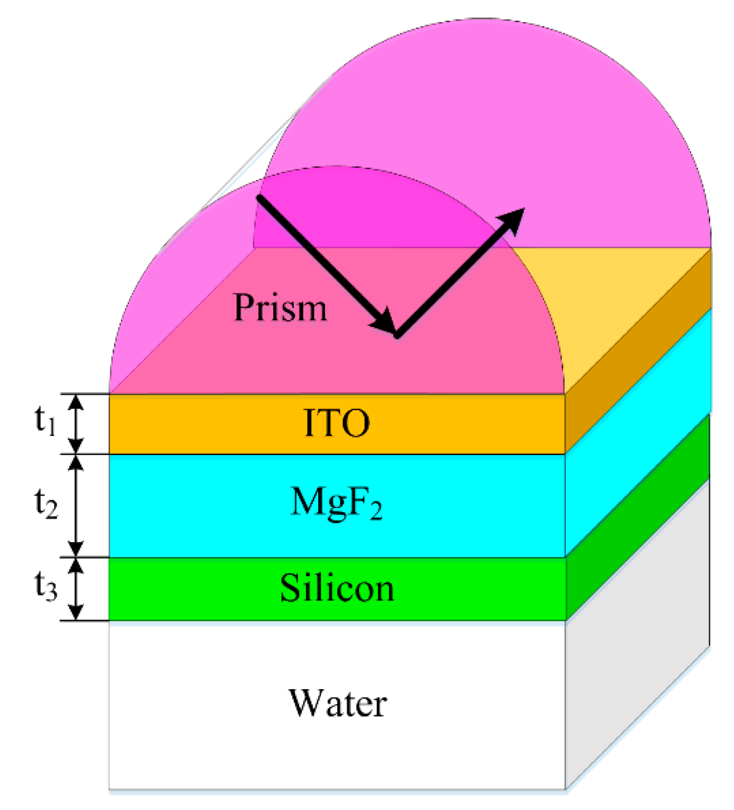
The proposed structure is schematically shown in Figure 1. The Kretschmann configuration consists of a rutile prism, an ITO layer with thickness t1, an MgF2 layer with thickness t2, a silicon layer with thickness t3 semi-infinitely surrounded by water. In this configuration, the ITO-MgF2 interface supports the SPP mode while PWG mode can exist in the planar waveguide formed by MgF2-silicon-water. When the SPP mode excited by the p-polarized light from a prism at 1550 nm wavelength is propagating along the ITO-MgF2 interface, the tail of the SPP evanescent field overlaps the one of the PWG mode, resulting in the coupling between these two modes. The coupling strength is determined by the thickness of MgF2 layer.
In this paper, for SPR curve calculation and sensing performance analysis, transfer matrix method is employed [6].
In the proposed structure, all layers stack along in the z-direction and each layer is defined by their thickness tk, refractive index nk and dielectric constant εk. The tangential fields at first boundary is set as Z = Z1 = 0, and the relation of tangential fields between first and final boundary Z = ZN−1 is given as
where U1 and V1 are, respectively, the electric and magnetic fields at the boundary of first layer, UN−1 and VN−1 are respectively the electric and magnetic at the boundary of the Nth layer. M is the characteristic transfer matrix of the combined N-layer structure. M is given as
with
where
and
Here, θ1 is the incident angle. Appling the transfer matrix method for N-layer model, we can obtain four elements M11, M12, M21, and M22 of M. Using these elements to calculate the total reflection coefficient rp for p-polarization light, we can get the relation as
and the phase (ϕp) of N-layer model for p-polarization is obtained by
It is known that SPR only affects p-polarization light, therefore s-polarization light can be served as a reference signal to eliminate environmental noises for improving the stability and accuracy of SPR sensors throughout the measurement. For s-polarization light the above equations hold except
and the differential phase between p- and s-polarization is obtained as
In the proposed structure, the water acts as the sensing medium and the refractive index (IR) change induced by biomolecules is denoted by Δn. Consequently, the intensity sensitivity can be defined as
where ΔRp =|rp|2 represents the reflectivity of the p-polarization light at incident angle θ. While the phase sensitivity is defined as
where Δφd is the differential phase changes between p-polarization light and s-polarization light with index variation of Δn. The refractive index of the rutile prism, ITO, MgF2, silicon, and pure water are chosen to be 2.453 [29], 0.267 + 1.912i [30], 1.3705 [31], 3.4764 [32], and 1.33, respectively.
3. Results and Discussions
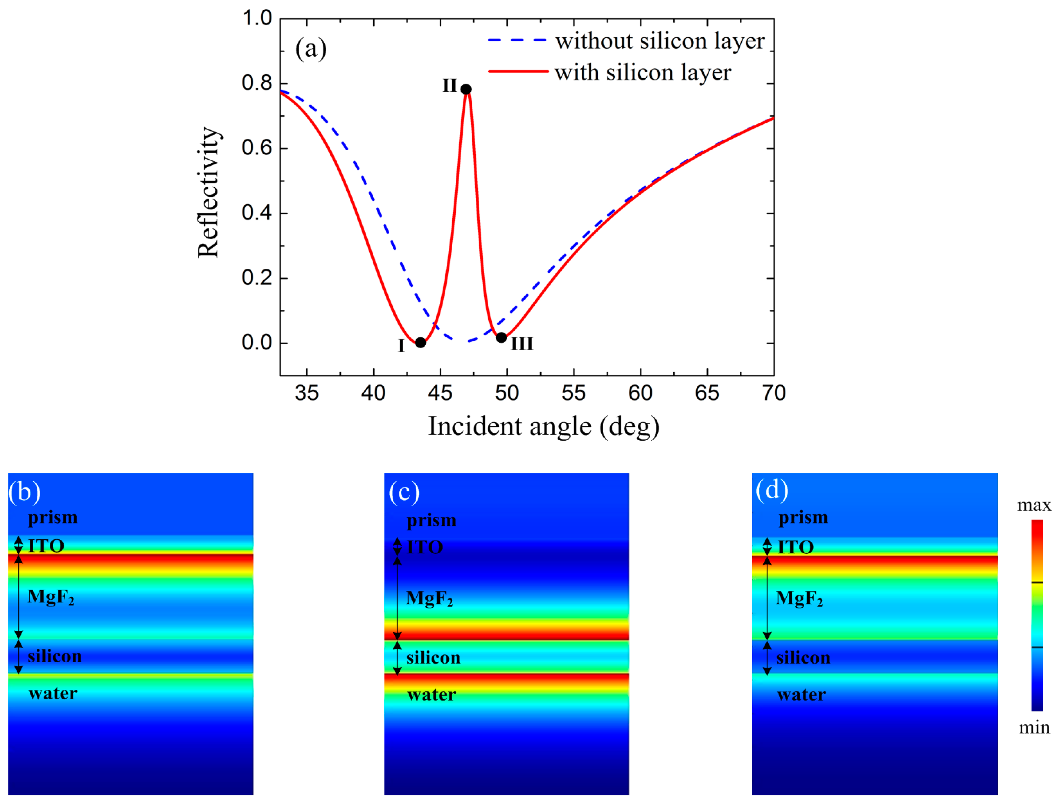
When the silicon layer is absent, the structure represents a typical SPR sensor. With an ITO thickness of 110 nm, the attenuated total reflection (ATR) curve as a function of incident angle from prism is shown as the blue one in Figure 2a. The minimum reflectivity appears at the angle of 46.7°, indicating the efficient excitation of SPP mode at the ITO-MgF2 interface. In this condition, the SPP mode cannot couple with PWG mode because of the absence of photonic waveguide. However, with the existence of the high index silicon layer, the situation can be changed. With MgF2 thickness t2 = 500 nm and silicon thickness t3 = 200 nm, the ATR curve is shown as the red one in Figure 2a. A sharp peak with high reflectivity appears near the resonant dip of the broad ATR curve which is similar to the response of a typical EIT system. With this sharp reflection peak, the single resonance dip is split into two, as Points I and III in Figure 2a. To further explain the properties of the EIT-like performance, the distributions of electric magnitude |E| at the two reflection dips (labelled as I and III) and the reflection peak (labelled as II) are illustrated in Figure 2b–d. It can be found that at two reflection dips, the SPP mode and PWG mode couple with each other and consequently form two hybrid modes upon the excitation light with incident angle of 43.4° and 49.6°, respectively. However, at the angle of transparency peak, Figure 2c, only the PWG mode is excited and therefore the absorption from the ITO layer is strongly suppressed. This is similar to the EIT effect in atom system, cancelling of the bright mode due to the destructive interference of two pathways [33]. More specifically, in the proposed structure, the SPP mode serves as the bright mode while the PWG mode acts as dark mode. The two pathways are incident light → SPP mode and incident light → SPP mode → PWG mode → SPP mode, respectively.
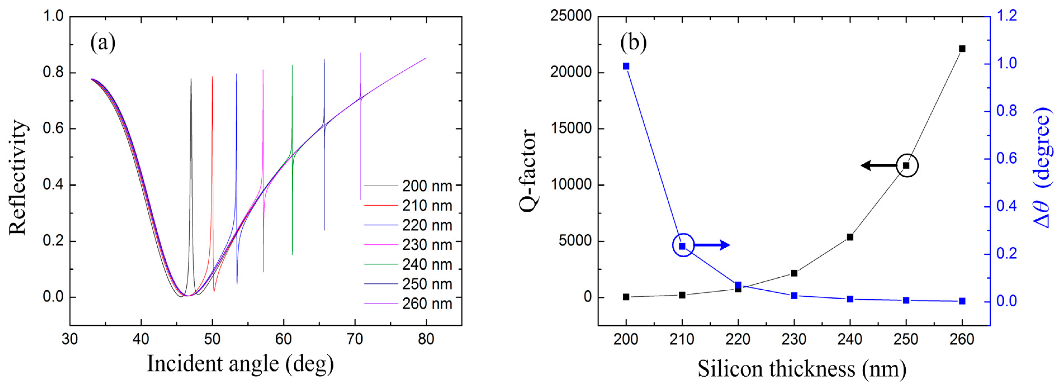
To obtain FR line shape, the resonant angle of the PWG mode can be designed to diverge from the one of SPP mode. This can be achieved by adjusting the thickness of the silicon layer so as to changing the effective index of the PWG mode. For this purpose, the ATR curves with different silicon thicknesses under the condition of t1 = 110 nm and t2 = 700 nm are calculated and shown in Figure 3a. With increased silicon thickness, the transparency peak moves to larger incident angle. This is because thicker silicon layer corresponds to higher effective index of the PWG mode, consequently, larger incident angles are required to match the resonant condition. Additionally, the asymmetric line of the resonance becomes the typical FR shape with a resonant peak and a resonant dip locating at the low- and high-angle sides, respectively. The difference of the FR dip and peak (Δθ), and the Q-factor (defined as θ/Δθ, where θ is the resonant angle of FR) are demonstrated in Figure 3b. It can be found that with thicker silicon, Δθ of the resonance decreases and leads to higher Q-factor. Later, we will show that the larger Q-factor corresponds to higher phase sensitivity.
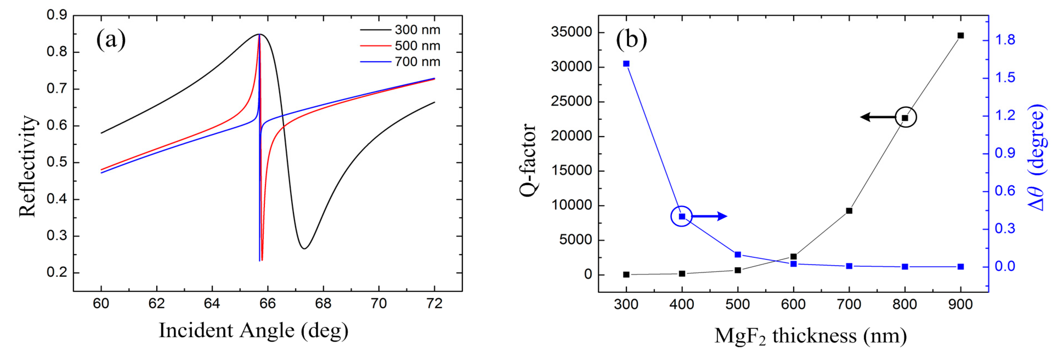
We also study the influence of MgF2 thickness on the reflection property. With t1 = 110 nm and t3 = 250 nm, the ATR curves with 300, 500, and 700 nm MgF2 thicknesses are illustrated in Figure 4a. In the proposed structure, the MgF2 layer behaves as the coupling layer. The coupling is stronger with thinner MgF2 layer and vice versa. As typical FR, with stronger coupling, the resonance becomes broader, resulting in a lower Q-factor, as shown in Figure 4b.
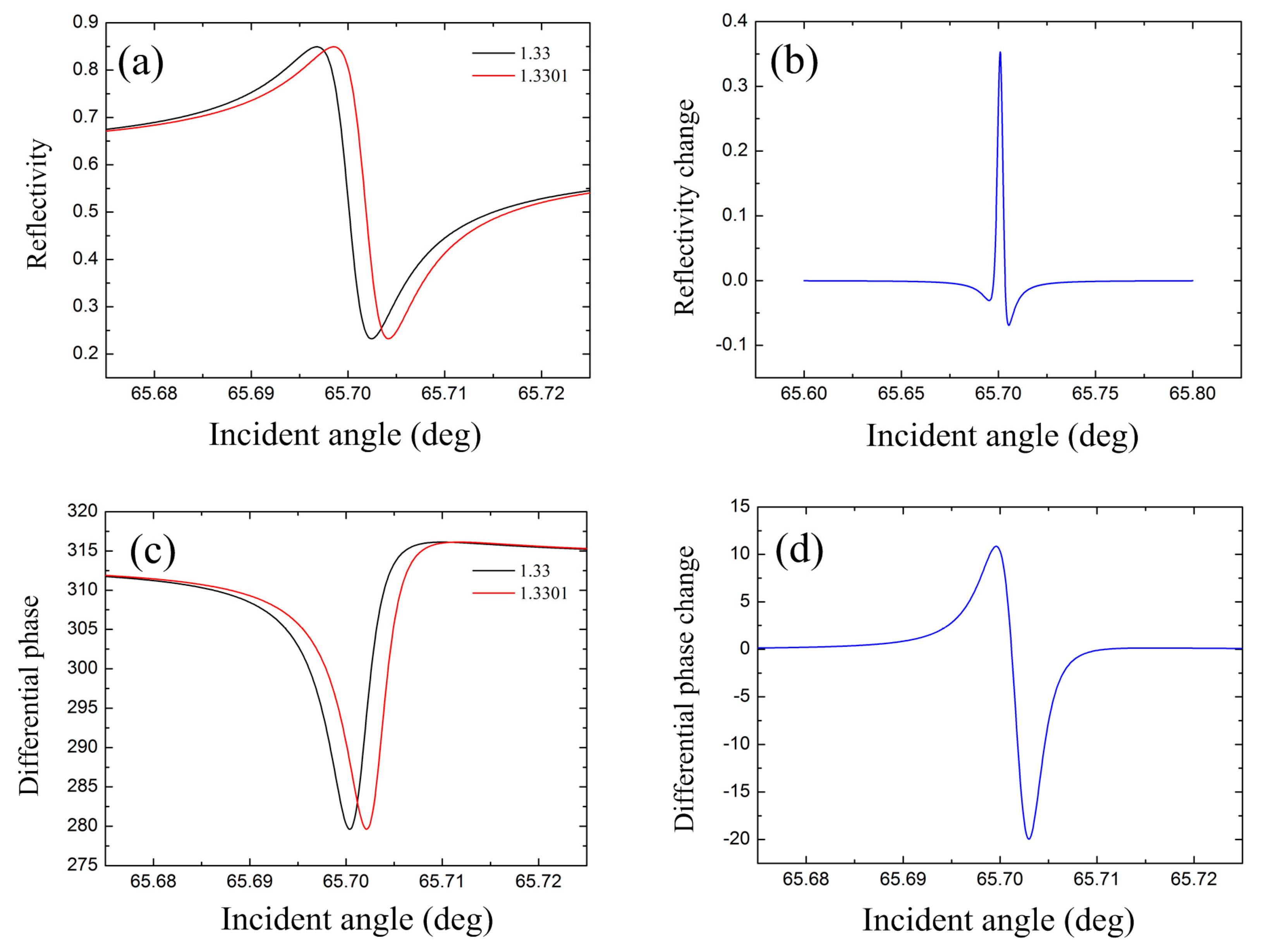
To investigate the sensing performance, the structure parameters are firstly set with t1 = 110 nm, t2 = 700 nm, and t3 = 250 nm. The ATR curves with surrounded RI of 1.33 and 1.3301 are shown in Figure 5a. With higher RI, the resonance moves towards larger incident angle. The sharp transition region between resonance peak and resonance dip is preferred for sensing applications with intensity interrogation. The reflectivity change is demonstrated in Figure 5b. The maximum appears at angle of 65.701°, indicating an intensity sensitivity of 3.5 × 10³ RIU−1. When considering the phase sensitivity of the structure, both p-polarized and s-polarized waves are launched into the structure simultaneously. Because only the p-polarized light experiences a significant phase jump, phase information is extracted from an interference pattern between the ‘probe’ p-polarized beam and the ‘reference’ s-polarized beam reflected from the sensor. The change of differential phase is monitored with the RI variation of the water. The curves of differential phase with surrounded RI of 1.33 and 1.3301 are shown in Figure 5c. It can be found that there is a dip for the differential phase with two sharp edges. Therefore, with fixed incident angle near these edges, the differential phase variation can be employed to sense the RI change. As shown in Figure 5d, the maximum differential phase variation of 20° with RI changing from 1.33 to 1.3301 appears at incident angle of 65.703°. According to the definition of phase sensitivity, the phase sensitivity is as high as 2 × 10⁵ degree/RIU. Furthermore, it should be noted that at the angle of 65.703° with the highest sensitivity, the reflectivity of p-polarized incident light is still as high as 24% and 29.5% under RI of 1.33 and 1.3301, respectively. This is different from conventional SPR sensors. Under SPR, Fresnel’s formulae theoretically predicts infinite Heaviside-like phase jump by properly optimizing the metal thickness [7]. Furthermore, it has been verified that, under pure SPR response in a Kretschmann configuration, the phase jump at the resonance angle is only dependent on the minimum reflectivity. The highest phase sensitivity is appeared at the angle where the reflection is lowest [6,7,8]. However, in practice, the reflectivity of p-polarized light cannot be lower than 1% to 4% so that it can be detected by the photodiode. Therefore, the incident angle should slightly diverge from the one with maximum phase sensitivity [8]. In our FR-based approach, benefiting from the high reflectivity, it is no need to change the incident angle and the maximum phase sensitivity can be directly employed in practical applications. Considering a typical detectable phase of 0.001 deg in phase-sensitive SPR sensors [7], the low-detection limit of the proposed FR-based sensor approaches the order of 10−9 RIU. Furthermore, it should be noted that this detectable phase of 0.001 deg is usually obtained under the SNR around 3:1 in conventional SPR sensors. In the proposed configuration, the reflectivity (24–29.5%) is five times higher than that of conventional SPR sensors (1–4%), and therefore even better performance can be expected with such signal power level. Furthermore, high reflectivity is also essential to reduce the power consumption of the sensor.
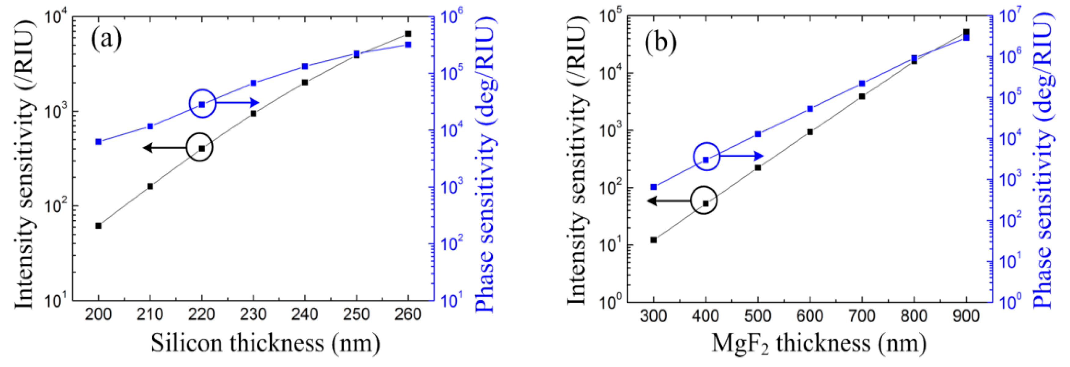
The sensing performance with different silicon layer thicknesses is demonstrated in Figure 6a. Both the intensity sensitivity and phase sensitivity are enhanced with thicker silicon layer. The sensitivities can also be increased proportionally with the thickness of MgF2 layer, as shown in Figure 6b. More generally, larger Q-factor corresponds to higher sensitivity. With t2 = 900 nm and t3 = 250 nm, the intensity sensitivity and phase sensitivity can achieve 104 RIU−1 and 106 deg/RIU, respectively. In this condition, the skin-depth at the silicon–water interface is about 135 nm. The phase sensitivity is comparable to conventional SPR sensors that are excited with a much larger minimum reflectivity value [7,34,35]. However, it should be mentioned that, the sensitivity cannot increase infinitely, since the line shape will be too narrow to be detected considering a typical angular resolution of 0.001 deg. Furthermore, the extremely high sensitivity will make the sensor’s resolution approach the limit of shot noise. Therefore, the main purpose of this investigation is to provide a methodology for sensor performance engineering. The detailed noise analysis is beyond the scope of this work.
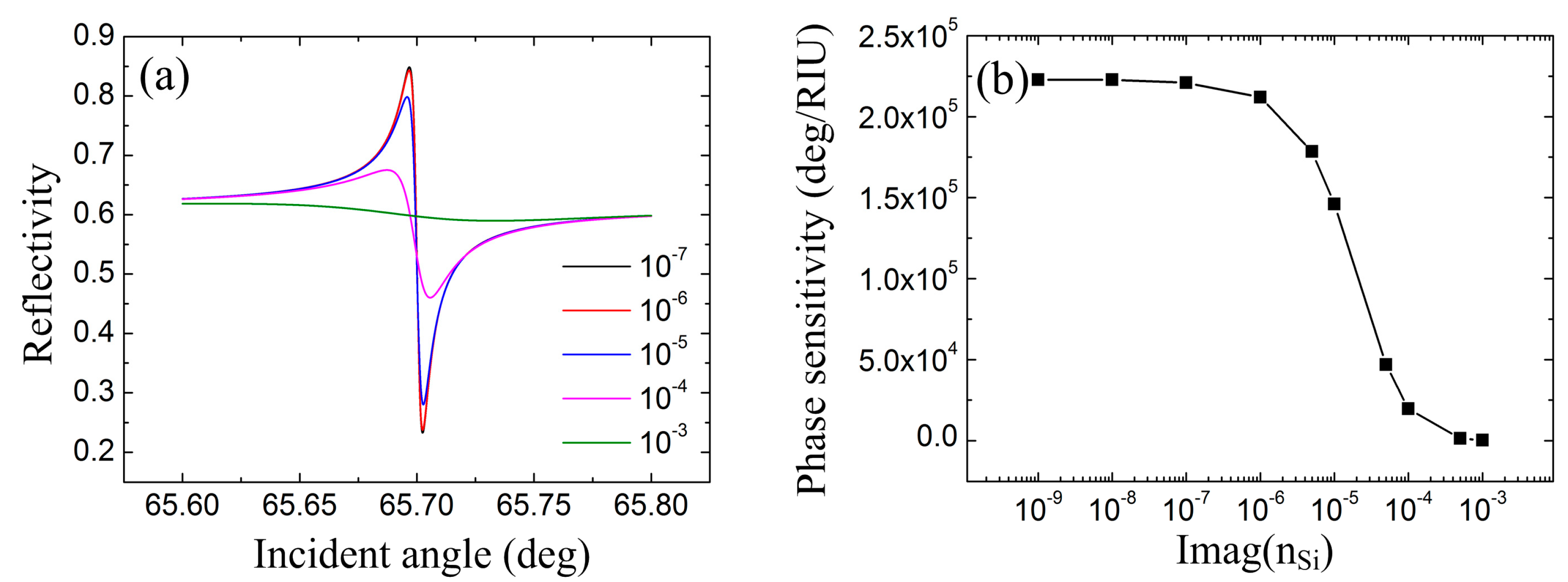
Note that the damping rate of the PWG mode is directly related to the characteristics of the resonance. In this paper, we employ ITO to support SPP mode in the near-infrared region where silicon demonstrates much lower absorption comparing with visible wavelength. However, the loss of the silicon waveguide is still quite dependent on the fabrication process. For this purpose, the imaginary part of the silicon refractive index imag(nSi) is varied to investigate the sensing performances under different damping rate of the PWG mode. With the MgF2 layer and the silicon layer fixed to be 700 nm and 250 nm, the total internal reflection spectra with respected to imag(nSi) are demonstrated in Figure 7a. The transition region of FR is steeper with lower loss. When imag(nSi) approaches 10−3, the FR line shape almost disappears. However, the locations of minimum reflectivity and maximum reflectivity are almost unchanged once imag(nSi) is smaller than 10−6, which means the Q-factor is unchanged as well. This phenomenon is consistent with the phase sensitivity, as illustrated in Figure 7b. It is found that the phase sensitivity changes little with imag(nSi) lower than 10−6 which corresponds to a loss of ~0.35 dB/cm. This requirement can be fulfilled by current fabrication technology [36]. Overall, since both ITO and silicon are CMOS-compatible, the multilayer structure can be fabricated through a conventional ‘bottom-up’ process.
4. Conclusions
In summary, we propose a waveguide-coupled SPR system for refractive index sensing at NIR regime using ITO as the plasmonic material. The coupling between SPP mode and PWG mode results in strong FR. Similar with SPR, it is found that the differential phase between p-polarized mode reflected light and s-polarized reflected light near FR is highly dependent on the index change of the surrounding medium, which offers great potential for phase-sensitive detection. The phase sensitivity can be engineered to a very high value by adjusting the thickness of MgF2 and silicon. More importantly, such high sensitivity is obtained without sacrificing reflectivity comparing to conventional SPR sensors. Therefore, the proposed scheme can be a promising candidate for biosensing applications with high accuracy and low power consumption.
Author Contributions
Conceptualization, Z.C.; Methodology, T.H. and S.Z.; Software, X.Z.; Validation, T.H. and S.Z.; Formal Analysis, X.Z.; Investigation, P.S.P.; Resources, P.S.P.; Data Curation, X.X.; Writing-Original Draft Preparation, T.H.; Writing-Review & Editing, S.Z.; Supervision, Z.C.; Project Administration, X.Z.; Funding Acquisition, Z.C., T.H. and S.Z.
Funding
This research was partially funded by the National Natural Science Foundation of China under grant number 61605179; Wuhan Science and Technology Project under grant number 2018010401011297; European Union’s Horizon 2020 research and innovation programme, Marie Sklodowska-Curie grant under grant number 798916; Fundamental Research Funds for the Central Universities, China University of Geosciences (Wuhan) under grant numbers 162301132703, G1323511794, and CUG2018JM16; and the Experimental Technology Research Funds under grant number SJ-201816.
Acknowledgments
In this section you can acknowledge any support given which is not covered by the author contribution or funding sections. This may include administrative and technical support, or donations in kind (e.g., materials used for experiments).
Conflicts of Interest
The authors declare no conflict of interest.
References
- Zeng, S.; Baillargeat, D.; Ho, H.-P.; Yong, K.-T. Nanomaterials enhanced surface plasmon resonance for biological and chemical sensing applications. Chem. Soc. Rev. 2014, 43, 3426–3452. [Google Scholar] [CrossRef] [PubMed]
- Hoa, X.D.; Kirk, A.G.; Tabrizian, M. Towards integrated and sensitive surface plasmon resonance biosensors: A review of recent progress. Biosens. Bioelectron. 2007, 23, 151–160. [Google Scholar] [CrossRef] [PubMed]
- Zijlstra, P.; Paulo, P.M.R.; Orrit, M. Optical detection of single non-absorbing molecules using the surface plasmon resonance of a gold nanorod. Nat. Nanotechnol. 2012, 7, 379–382. [Google Scholar] [CrossRef] [PubMed] [Green Version]
- Huang, Y.H.; Ho, H.P.; Kong, S.K.; Kabashin, A.V. Phase-sensitive surface plasmon resonance biosensors: Methodology, instrumentation and applications. Ann. Phys. 2012, 524, 637–662. [Google Scholar] [CrossRef]
- Zeng, S.; Sreekanth, K.V.; Shang, J.; Yu, T.; Chen, C.K.; Yin, F.; Baillargeat, D.; Coquet, P.; Ho, H.P.; Kabashin, A.V.; et al. Graphene-gold metasurface architectures for ultrasensitive plasmonic biosensing. Adv. Mater. 2015, 27, 6163–6169. [Google Scholar] [CrossRef] [PubMed]
- Zeng, S.; Hu, S.; Xia, J.; Anderson, T.; Dinh, X.Q.; Meng, X.M.; Coquet, P.; Yong, K.T. Graphene–MoS2 hybrid nanostructures enhanced surface plasmon resonance biosensors. Sens. Actuators B Chem. 2015, 207, 801–810. [Google Scholar] [CrossRef]
- Kabashin, A.V.; Patskovsky, S.; Grigorenko, A.N. Phase and amplitude sensitivities in surface plasmon resonance bio and chemical sensing. Opt. Express 2009, 17, 21191–21204. [Google Scholar] [CrossRef] [PubMed]
- Kravets, V.G.; Schedin, F.; Jalil, R.; Britnell, L.; Gorbachev, R.V.; Ansell, D.; Thackray, B.; Novoselov, K.S.; Geim, A.K.; Kabashin, A.V.; et al. Singular phase nano-optics in plasmonic metamaterials for label-free single-molecule detection. Nat. Mater. 2013, 12, 304–309. [Google Scholar] [CrossRef] [PubMed] [Green Version]
- Ong, B.H.; Yuan, X.; Tjuin, S.C.; Zhang, J.; Ng, H.M. Optimized film thickness for maximum field enhancement of a bimetallic surface plasmon resonance biosensor. Sens. Actuators B Chem. 2006, 114, 1028–1034. [Google Scholar] [CrossRef]
- Ran, B.; Lipson, S.G. Comparison between sensitivities of phase and intensity detection in surface plasmon resonance. Opt. Express 2006, 14, 5641–5650. [Google Scholar] [CrossRef] [PubMed]
- Watad, I.; Abdulhalim, I. Spectropolarimetric Surface Plasmon Resonance Sensor and the Selection of the Best Polarimetric Function. IEEE J. Sel. Top. Quantum Electron. 2017, 23, 89–97. [Google Scholar] [CrossRef]
- Watad, I.; Abdulhalim, I. Comparative study between polarimetric and intensity based surface plasmon resonance sensors in the spectral mode. Appl. Opt. 2017, 56, 7549–7558. [Google Scholar] [CrossRef] [PubMed]
- López-Tejeira, F.; Pániagua-Dominguez, R.; Sánchez-Gil, A. High-performance nanosensors based on plasmonic Fano-like interference: Probing refractive index with individual nanorice and nanobelts. ACS Nano 2012, 6, 8989–8996. [Google Scholar] [CrossRef] [PubMed]
- Lu, H.; Liu, X.; Mao, D.; Wang, G. Plasmonic nanosensor based on Fano resonance in waveguide-coupled resonators. Opt. Lett. 2012, 37, 3780–3782. [Google Scholar] [CrossRef] [PubMed]
- Chen, J.; Sun, C.; Gong, Q. Fano resonances in a single defect nanocavity coupled with a plasmonic waveguide. Opt. Lett. 2014, 39, 52–55. [Google Scholar] [CrossRef] [PubMed]
- Hayashi, S.; Nesterenko, D.V.; Sekkat, Z. Fano resonance and plasmon-induced transparency in waveguide-coupled surface plasmon resonance sensors. Appl. Phys. Express 2015, 8, 022201. [Google Scholar] [CrossRef]
- Hayashi, S.; Nesterenko, D.V.; Sekkat, Z.; Rahmouni, A. Observation of Fano line shapes arising from coupling between surface plasmon polariton and waveguide modes. Appl. Phys. Lett. 2016, 108, 051101. [Google Scholar] [CrossRef]
- Wu, C.; Ding, H.; Huang, T.; Wu, X.; Chen, B.; Ren, K.; Fu, S. Plasmon-induced transparency and refractive index sensing in side-coupled stub-hexagon resonators. Plasmonics 2018, 13, 251–257. [Google Scholar] [CrossRef]
- Nesterenko, D.V.; Hayashi, S.; Sekkat, Z. Extremely narrow resonances, giant sensitivity and field enhancement in low-loss waveguide sensors. J. Opt. 2016, 18, 065004. [Google Scholar] [CrossRef]
- Wu, L.; Guo, J.; Xu, H.; Dai, X.; Xiang, Y. Ultrasensitive biosensors based on long-range surface plasmon polariton and dielectric waveguide modes. Photonics Res. 2016, 4, 262–266. [Google Scholar] [CrossRef]
- Geddes, C.D. Reviews in Plasmonics; Springer: New York, NY, USA, 2010. [Google Scholar]
- Rizal, C.; Pisana, S.; Hrvoic, I. Improved magneto-optic surface plasmon resonance biosensors. Photonics 2018, 5, 15. [Google Scholar] [CrossRef]
- Rizal, C.; Pisana, S.; Hrvoic, I.; Fullerton, E.E. Microstructure and magneto-optical surface plasmon resonance of Co/Au multilayers. J. Phys. Commun. 2018, 5, 055010. [Google Scholar] [CrossRef]
- Rizal, C.; Moa, B.; Niraula, B.B. Ferromagnetic Multilayers: Magnetoresistance, Magnetic Anisotropy, and Beyond. Magnetochemistry 2016, 2, 22. [Google Scholar] [CrossRef]
- Silveirinha, M.G.; Engheta, N. Transporting an image through a subwavelength hole. Phys. Rev. Lett. 2009, 102, 103902. [Google Scholar] [CrossRef] [PubMed]
- Alù, A.; Engheta, N. Cloaking a sensor. Phys. Rev. Lett. 2009, 102, 233901. [Google Scholar]
- Liu, K.; Ye, C.R.; Khan, S.; Sorger, V.J. Review and perspective on ultrafast wavelength-size electro-optic modulators. Laser Photonics Rev. 2015, 9, 172–194. [Google Scholar] [CrossRef]
- Lee, H.W.; Papadakis, G.; Burgos, S.P.; Chander, K.; Kriesch, A.; Pala, R.; Peschel, U.; Atwater, H.A. Nanoscale conducting oxide PlasMOStor. Nano Lett. 2014, 14, 6463–6468. [Google Scholar] [CrossRef] [PubMed]
- Thorlabs. Available online: www.thorlabs.com (accessed on 9 August 2018).
- Patnaik, A.; Senthilnathan, K.; Jha, R. Graphene-based conducting metal oxide coated D-shaped optical fiber SPR sensor. IEEE Photonics Technol. Lett. 2015, 27, 2437–2440. [Google Scholar] [CrossRef]
- Dodge, M.J. Refractive properties of magnesium fluoride. Appl. Opt. 1984, 23, 1980–1985. [Google Scholar] [CrossRef] [PubMed]
- Palik, E.D. Handbook of Optical Constants of Solids; Academic: San Diego, CA, USA, 1998. [Google Scholar]
- Boller, K.J.; Imamolu, A.; Harris, S.E. Observation of electro-magnetically induced transparency. Phys. Rev. Lett. 1991, 66, 2593–2596. [Google Scholar] [CrossRef] [PubMed]
- Patskovsky, S.; Song, I.H.; Meunier, M.; Kabashin, A.V. Silicon based total internal reflection bio and chemical sensing with spectral phase detection. Opt. Express 2009, 17, 20847–20852. [Google Scholar] [CrossRef] [PubMed]
- Ouyang, Q.L.; Zeng, S.W.; Jiang, L.; Hong, L.Y.; Xu, G.X.; Dinh, X.Q.; Qian, J.; He, S.L.; Qu, J.L.; Coquet, P.; Yong, K.T. Sensitivity enhancement of transition metal dichalcogenides/silicon nanostructure-based surface plasmon resonance biosensor. Sci. Rep. 2016, 6, 28190. [Google Scholar] [CrossRef] [PubMed]
- Rickman, A. The commercialization of silicon photonics. Nat. Photonics 2014, 8, 579–582. [Google Scholar] [CrossRef]
Figure 1.
Schematic diagram of the SPR sensor.

Figure 2.
(a) The attenuated total reflection curves with and without silicon layer, |E| distributions at point (b) I, (c) II, and (d) III.
Figure 2.
(a) The attenuated total reflection curves with and without silicon layer, |E| distributions at point (b) I, (c) II, and (d) III.

Figure 3.
(a) ATR curves with different silicon thicknesses, and (b) Q-factor and the Δθ of FR with different silicon thicknesses. The ITO and MgF2 thicknesses t1 and t2 are fixed to be 110 nm and 700 nm, respectively.
Figure 3.
(a) ATR curves with different silicon thicknesses, and (b) Q-factor and the Δθ of FR with different silicon thicknesses. The ITO and MgF2 thicknesses t1 and t2 are fixed to be 110 nm and 700 nm, respectively.

Figure 4.
(a) ATR curves with different MgF2 thicknesses, and (b) Q-factor and the Δθ of FR with different MgF2 thicknesses. The ITO and silicon thicknesses t1 and t3 are fixed to be 110 nm and 250 nm, respectively.
Figure 4.
(a) ATR curves with different MgF2 thicknesses, and (b) Q-factor and the Δθ of FR with different MgF2 thicknesses. The ITO and silicon thicknesses t1 and t3 are fixed to be 110 nm and 250 nm, respectively.

Figure 5.
(a,c) Reflectivity and differential phase versus incident angle under probing sampling RI of 1.33 and 1.3301, and (b,d) the corresponding reflectivity and differential phase change. (t1 = 110 nm, t2 = 700 nm, and t3 = 250 nm).
Figure 5.
(a,c) Reflectivity and differential phase versus incident angle under probing sampling RI of 1.33 and 1.3301, and (b,d) the corresponding reflectivity and differential phase change. (t1 = 110 nm, t2 = 700 nm, and t3 = 250 nm).

Figure 6.
Sensing performance versus (a) silicon layer thickness with MgF2 thickness fixed to be 700 nm, and (b) MgF2 layer thickness with silicon thickness fixed to be 250 nm.
Figure 6.
Sensing performance versus (a) silicon layer thickness with MgF2 thickness fixed to be 700 nm, and (b) MgF2 layer thickness with silicon thickness fixed to be 250 nm.

Figure 7.
(a) ATR curves near FR angle and (b) phase sensitivity with considering different imag(nSi).
Figure 7.
(a) ATR curves near FR angle and (b) phase sensitivity with considering different imag(nSi).

© 2018 by the authors. Licensee MDPI, Basel, Switzerland. This article is an open access article distributed under the terms and conditions of the Creative Commons Attribution (CC BY) license (http://creativecommons.org/licenses/by/4.0/).
Share and Cite
MDPI and ACS Style
Huang, T.; Zeng, S.; Zhao, X.; Cheng, Z.; Shum, P.P. Fano Resonance Enhanced Surface Plasmon Resonance Sensors Operating in Near-Infrared. Photonics 2018, 5, 23. https://doi.org/10.3390/photonics5030023
AMA Style
Huang T, Zeng S, Zhao X, Cheng Z, Shum PP. Fano Resonance Enhanced Surface Plasmon Resonance Sensors Operating in Near-Infrared. Photonics. 2018; 5(3):23. https://doi.org/10.3390/photonics5030023
Chicago/Turabian StyleHuang, Tianye, Shuwen Zeng, Xiang Zhao, Zhuo Cheng, and Perry Ping Shum. 2018. "Fano Resonance Enhanced Surface Plasmon Resonance Sensors Operating in Near-Infrared" Photonics 5, no. 3: 23. https://doi.org/10.3390/photonics5030023
Note that from the first issue of 2016, this journal uses article numbers instead of page numbers. See further details here.