Article

Pulsed Current Electrodeposition of Silicon Thin Films Anodes for Lithium Ion Battery Applications

by
Bharat Gattu
1,
Rigved Epur
2,
Pavithra Murugavel Shanti
1,
Prashanth Hanumantha Jampani
3,
Ramalinga Kuruba
3,
Moni Kanchan Datta
3,
Ayyakkannu Manivannan
4 and
Prashant N. Kumta
1,2,3,*
1
Department of Chemical and Petroleum Engineering, University of Pittsburgh, Pittsburgh, PA 15261, USA
2
Department of Mechanical Engineering and Materials Science, University of Pittsburgh, Pittsburgh, PA 15261, USA
3
Department of Bioengineering, University of Pittsburgh, Pittsburgh, PA 15261, USA
4
US Department of Energy, National Energy Technology Laboratory, Morgantown, WV 26507, USA
*
Author to whom correspondence should be addressed.
Inorganics 2017, 5(2), 27; https://doi.org/10.3390/inorganics5020027
Submission received: 20 March 2017 / Revised: 16 April 2017 / Accepted: 17 April 2017 / Published: 20 April 2017
(This article belongs to the Special Issue Novel Lithium Battery Electrode Materials)

Abstract

:
Electrodeposition of amorphous silicon thin films on Cu substrate from organic ionic electrolyte using pulsed electrodeposition conditions has been studied. Scanning electron microscopy analysis shows a drastic change in the morphology of these electrodeposited silicon thin films at different frequencies of 0, 500, 1000, and 5000 Hz studied due to the change in nucleation and the growth mechanisms. These electrodeposited films, when tested in a lithium ion battery configuration, showed improvement in stability and performance with an increase in pulse current frequency during deposition. XPS analysis showed variation in the content of Si and oxygen with the change in frequency of deposition and with the change in depth of these thin films. The presence of oxygen largely due to electrolyte decomposition during Si electrodeposition and the structural instability of these films during the first discharge–charge cycle are the primary reasons contributing to the first cycle irreversible (FIR) loss observed in the pulse electrodeposited Si–O–C thin films. Nevertheless, the silicon thin films electrodeposited at a pulse current frequency of 5000 Hz show a stable capacity of ~805 mAh·g−1 with a fade in capacity of ~0.056% capacity loss per cycle (a total loss of capacity ~246 mAh·g−1) at the end of 500 cycles.

Graphical Abstract

1. Introduction

Silicon is an important and widely used semiconductor material used in electronics industry as a major component of transistors, detectors, and microprocessors with a band gap of 1.1 eV. Over the last decade or so, efforts have been made to use silicon as anode in secondary lithium ion battery (LIB) systems replacing graphite, the traditional anode employed in the currently used Li-ion systems. This is attributed to the high theoretical specific charge storage capacity of silicon (4212 mAh·g−1) as compared to that of carbon/graphite (372 mAh·g−1) with respect to lithium [1,2,3]. However, the crystalline silicon anode suffers from colossal volumetric change (~320%) during the alloying and de-alloying in the LIB systems corresponding to the formation of Li22Si5 phase, causing severe mechanical stresses thus leading to deformation, cracking, and loss of inter-particle contact in the anode [4,5,6]. This behavior leads to catastrophic failure of the anode within the first few charge–discharge cycles, causing decripitation of the electrode leading to rapid capacity discharge [7,8,9,10,11] and consequent failure.
Amorphous silicon (a-Si) deposited at low temperatures has isotropic volumetric expansion during lithiation–delithiation reactions and is considered a more stable anode material as compared to crystalline silicon in LIB systems [8,9]. This is mainly due to the highly disordered structure causing more available free volume to be present, allowing for accommodation of the volume related stress and strain. a-Si in 2D form can be obtained by RF/magnetron sputtering from silicon targets, pulsed laser deposition, or thermal/plasma/microwave assisted decomposition of silicon precursors such as silane or organosilane precursors [12,13,14,15,16,17,18,19,20,21,22]. However, on an industrial scale these techniques are expensive, involve high installation/maintenance costs, and have major safety issues since they involve explosive Si precursors. RF/magnetron sputtering although a commercially viable method suffers from being a line of sight unidirectional deposition technique and hence, fails to provide complex nanostructured geometries which are often required to stabilize Si anode system in LIB.
Electrodeposition or electroplating is a relatively simple, easy, robust, easily scalable, and economically viable electrochemical technique for large area generation of active systems. It is very widely used in industries to synthesize coatings and thin films of various metals, alloys, and particulate composites to enhance the tribological and corrosion resistance properties of materials. Recently, electrodeposition of amorphous silicon (a-Si) from non-aqueous electrolytes has been used to deposit thin films and nanostructures of a-Si by potentiostatic (constant potential) and galvanostatic (constant current) methods on different substrates—such as nickel foams, nickel coated tobacco mosaic virus (TMV), and copper foil—and their electrochemical properties are studied for LIBs [23,24,25,26,27,28,29,30,31]. However, there is no reported study on the evolution and modification of the morphology of a-Si thin films during the electrodeposition process and the systems suffer from poor areal loading density, low areal capacities, and low overall specific capacity of the anode due to the type of substrates employed.
In this regard, pulse electrodeposition is a well-known modification of traditional electrodeposition process and has been studied for varying the morphology, mechanical properties and composition of different types of metallic, composite, and nano coatings [32,33,34,35]. The pulse power electrodeposition approach offers an economical and easy way to change the grain size and morphology of the deposits, thus enhancing the density of coatings and their mechanical strength and corrosion properties [36,37,38,39].
In the current work pulsed current electrodeposition (PED) technique was employed to develop Si thin films on Cu foil. PED at various frequencies of the pulsing cycle was used to obtain different morphologies of a-Si thin film deposits on Cu foil and their performance in LIB was studied. PED, which is a simple extension of electrodeposition technique, provides an economical way to modify the properties of the thin films by providing modulated voltage/current input into the electrodeposition cell instead of direct current or voltage. The composition and morphology of the thin films are thereby altered with the change in the frequency which correspondingly, influences their performance in the lithium ion batteries.

2. Results and Discussion

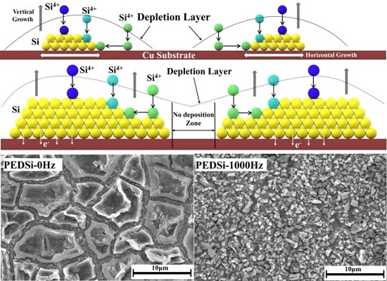
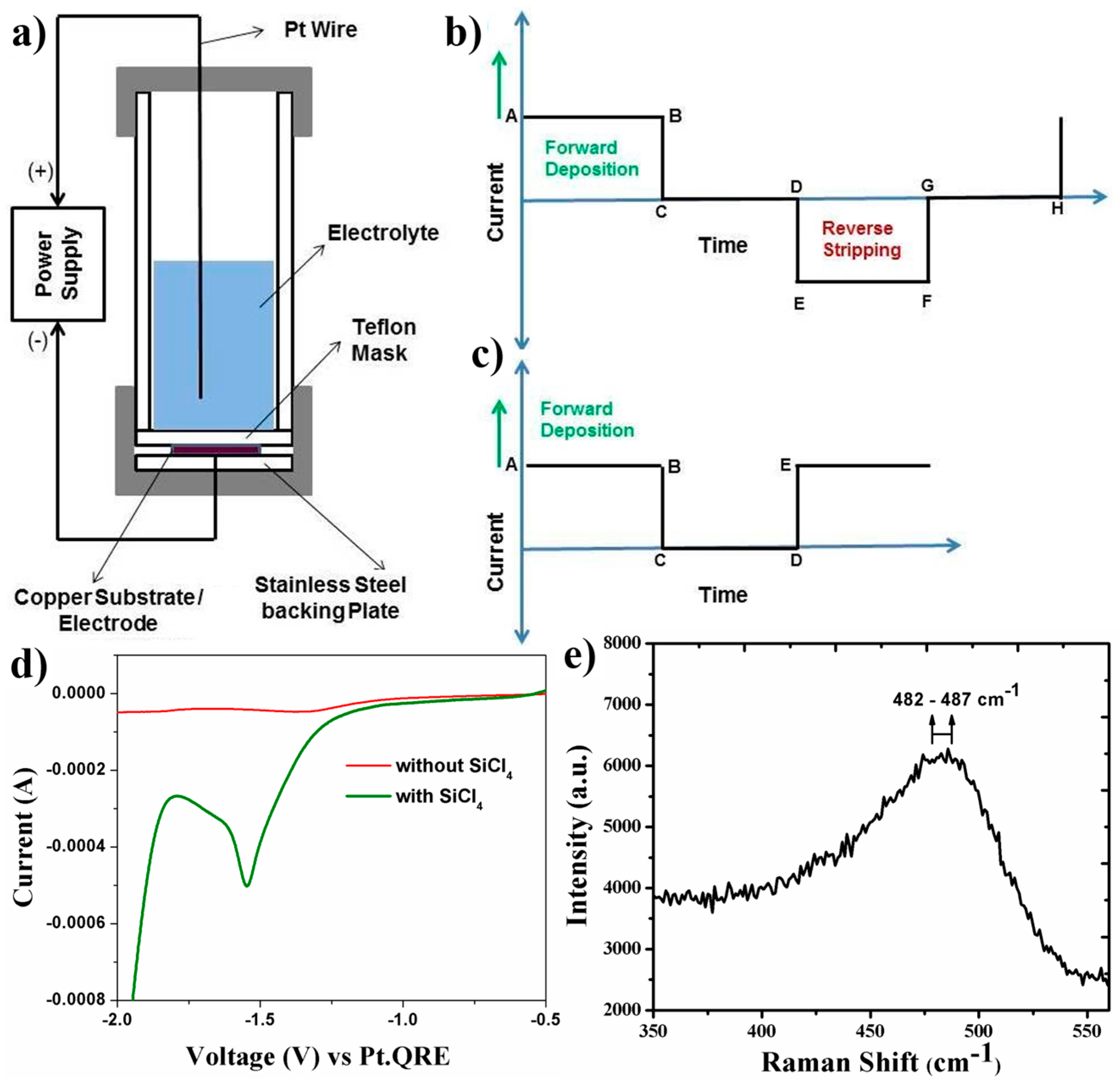
2.1. Pulsed Current Electrodeposition of Si on Cu Foils

The pictorial diagram of the two electrode electrodeposition cell along with the polarity of the electrical connections has been shown in Figure 1a. The general parameters of operation of the pulsed current electrodeposition are forward peak current density, forward ON TIME, forward OFF TIME, reverse peak current density, reverse ON TIME, reverse OFF TIME, and the total amount of charge supplied (Figure 1b). The reduction and deposition of Si4+ ions occurs during the ON TIME of the forward cycle (positive cycle) while during the ON TIME of the reverse cycle, the deposited Si is stripped in the form of Si4+ and enters the electrolyte solution. During the OFF TIME also, there is no current passing through the cell and hence, there is no reduction/oxidation taking place at the electrodes. However, during the OFF TIME, since there is no deposition occurring, there is diffusion of Si4+ ions from the bulk of the electrolyte towards the ionically depleted region formed at the electrode–electrolyte interface. A typical input cycle of pulse current electrodeposition with both deposition and stripping cycle is as shown in Figure 1b. In the current study however, to prevent the complications arising from the oxidation of Cu from the substrate into the electrolyte during the reverse cycle, we have employed only the forward deposition cycle as shown in Figure 1c. The percentage ratio of ON TIME (AB) to forward TIME (AB+CD) in the pulsing cycle is termed as the DUTY CYCLE and is kept constant at 50%. The different pulsed current electrodeposition parameters used in the study have been listed in Table 1.
The linear sweep voltammetry (Figure 1d) of the supporting electrolyte TBACL in propylene carbonate solvent showed stable electrolyte window of (−) 0.5 V to (−) 1.9 V without any deposition peak for the current electrochemical setup. With the addition of SiCl4, the LSV shows a cathodic peak corresponding to the reduction of Si4+ ions and deposition of Si at around (−) 1.58 V.
The pulse electrodeposited films showed yellowish color after they were washed in propylene carbonate followed by anhydrous acetone in the glove box atmosphere. However, upon exposure to ambient atmosphere, the silicon reacts with air/moisture and immediately undergoes oxidation to form silicon dioxide thus turning into a white deposit in due course of time. Hence, the electrodeposited samples were sealed in the glove box under argon atmosphere and then transferred for Raman analysis and into the scanning electron microscopy chamber for further analyses. The Raman analysis of all the pulse current electrodeposited films was carried within 15 min after exposure to ambient atmosphere. The Raman spectra showed a broad peak (Figure 1e), approximately 483–487 cm−1 for all the pulse electrodeposited samples. For crystalline silicon, a sharp peak corresponding to transverse optical vibrational mode is reported [40,41,42] at around 520 cm−1. However, the broad peak obtained in the Raman spectra suggests the presence of amorphous silicon in the thin film which is caused due to the disruption of long range order as compared to crystalline silicon.

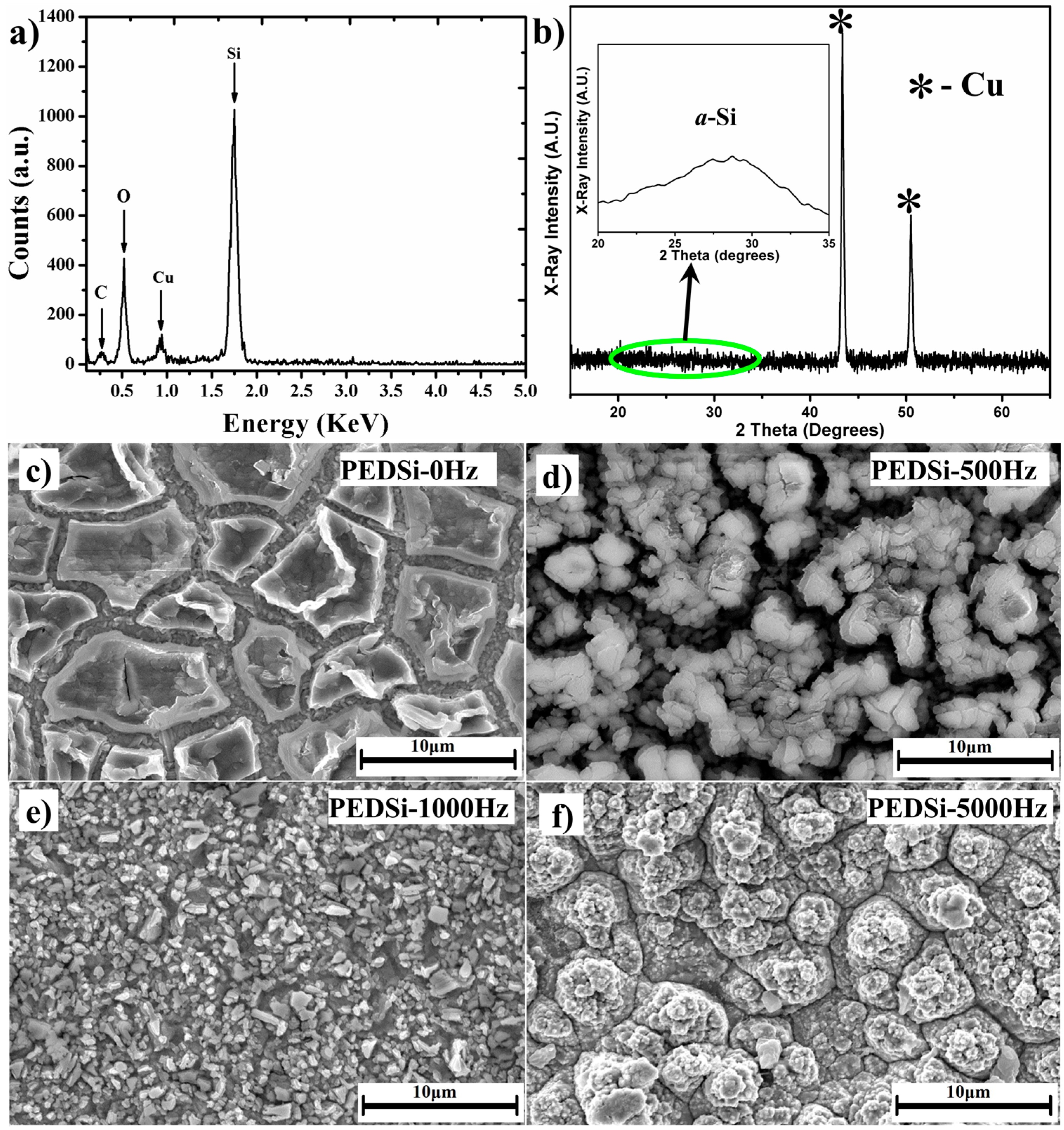
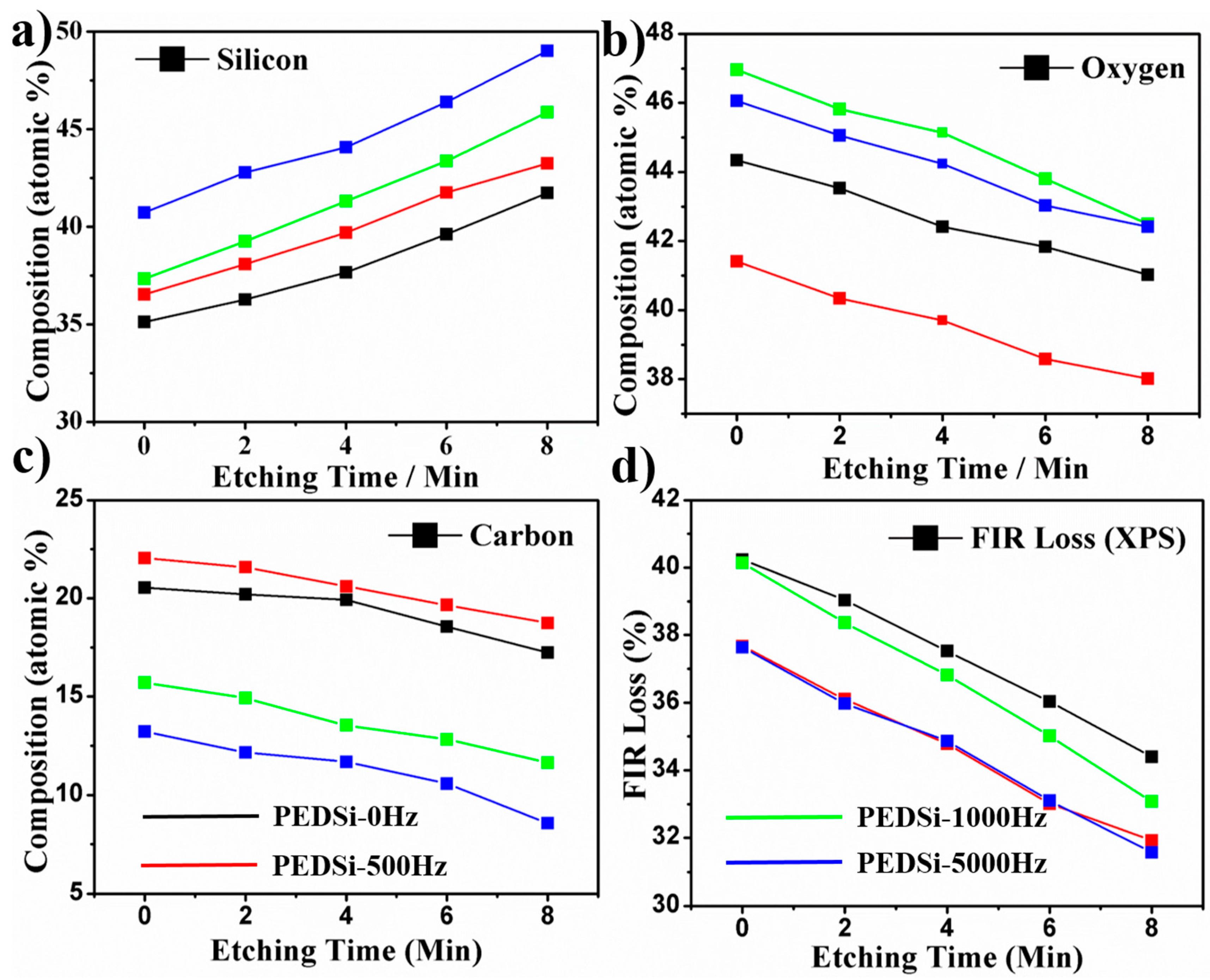
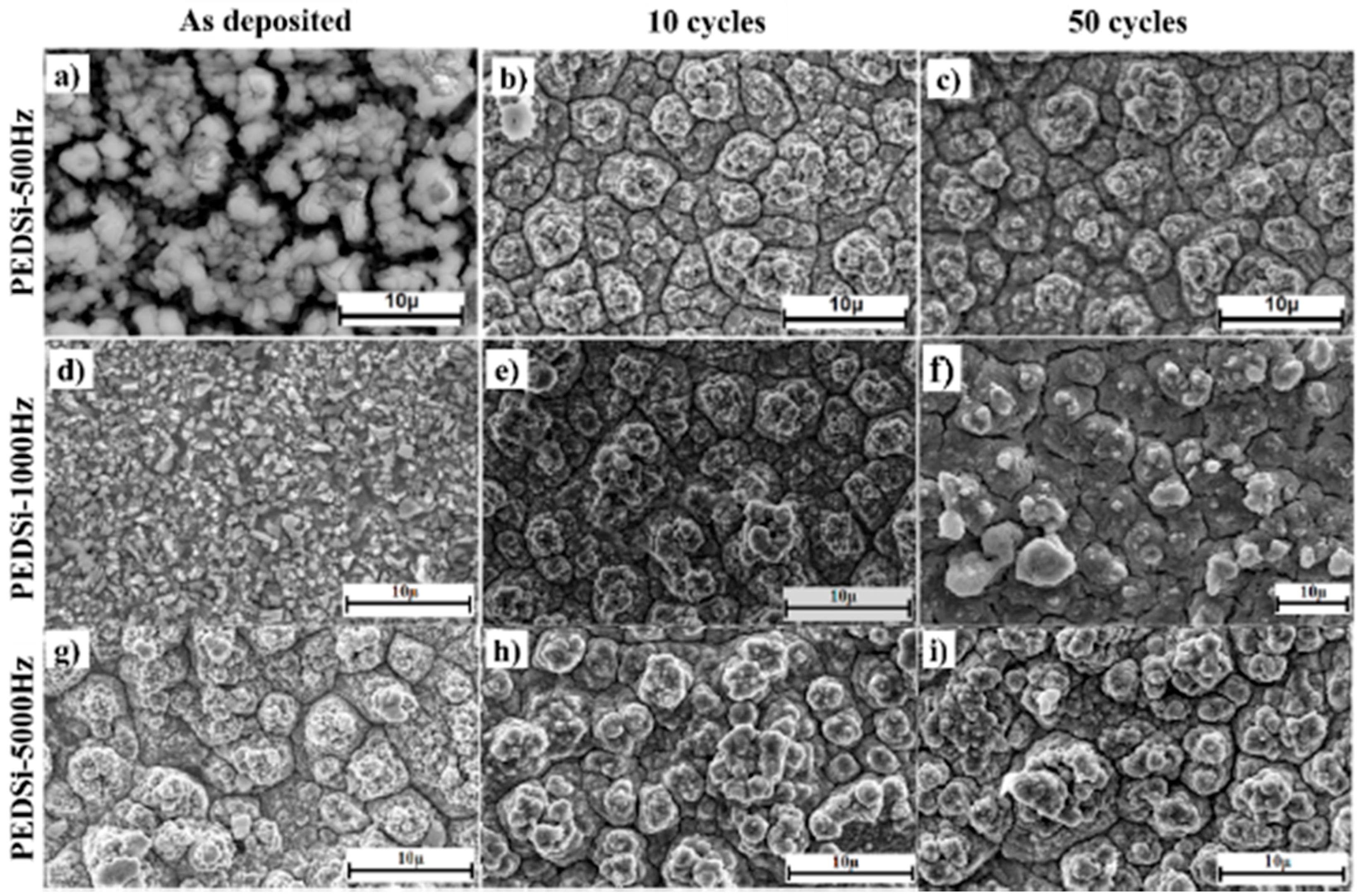
2.2. Morphological and Compositional Characterization

SEM analysis was conducted to observe the morphology of the electrodeposited films. For the SEM and EDAX analysis (Figure 2), the samples were transferred into the SEM chamber within 5 min of opening the seal to prevent the oxidation of silicon due to prolonged exposure to the oxygen and moisture in the room atmosphere. The EDAX analysis of the samples showed the presence of silicon, oxygen, copper, and carbon (Figutre 2a). The copper peak (CuLα ~0.93 KeV) arises from the substrate on which the electrodeposition has been carried out while the presence of oxygen is attributed to the partial oxidation of silicon (SiKα ~1.739 KeV) in the brief time the samples are exposed to the room atmosphere while transferring into the SEM chamber. The presence of carbon (CKα ~0.277 KeV) may be attributed to the presence of residual solvent or contamination from the SEM chamber. Another reason for the presence of carbon and oxygen (OKα ~0.525 KeV) can be attributed to the decomposition of electrolyte along with the reduction of silicon due to the localized over potential developed on the growth sites during the electrodeposition process, thus forming a Si–O–C composite system [43,44,45,46]. The glancing angle XRD pattern (Figure 2b) shows only Cu peaks (2θ ~43.7°, 50.8°) arising from the underlying substrate devoid of any peaks corresponding to crystalline silicon (high intensity peak at 2θ ~28.4°). The zoomed up inset pattern obtained from smoothening of the curves (inset of Figure 2b) shows a low intensity broad peak between 27° < 2θ < 30° which confirms the amorphous nature of electrodeposited silicon thin film validating the Raman analysis. Due to the amorphous nature of the silicon in the electrodeposited thin film, the intensity of the Cu peaks dominates the spectra obtained from the glancing angle XRD and the low intensity broad peak of a-Si could be noticed only by analyzing the obtained spectra in the 20° < 2θ < 35° region.
The SEM analysis (Figure 2) of the samples shows a drastic change in morphology between the films deposited at 0 (galvanostatic, PEDSi-0), 500 (PEDSi-500) and 1000 Hz (PEDSi-1000). PEDSi-0 (Figure 2c) which corresponds to the constant current electrodeposition showed islands of silicon approximately 5–10 μm wide simulating dried mud cracks, which is in good agreement with previous study reported [37]. PEDSi-500 (Figure 2d) which corresponds to pulse current frequency of 500 Hz, showed a cracked morphology very similar to PEDSi-0, however, the solid islands of Si were replaced by discrete particulate deposits. At a frequency of 1000 Hz, the island morphology was completely replaced with a thin continuous layer comprising of 1–2 μm silicon particles seen in the SEM analysis of PEDSi-1000 (Figure 2e). At higher frequency of 5000 Hz, the deposits retained the thin film morphology as observed in PEDSi-1000 however; the size of the particles comprising the film decreases to less than 1 μm observed in PEDSi-5000 (Figure 2f). This change in morphology occurs due to the change in the nucleation and growth kinetics of the film followed by the variation in thickness of the depletion layer at the electrode–electrolyte interface and the decrease in the concentration of ions in the bulk of the solution. The difference in the morphologies can be explained by two different reason depending on the frequencies used during pulse electrodeposition.
At lower frequencies (PEDSi-0 Hz, PEDSi-500 Hz, and PEDSi-1000 Hz), the competitive behavior between the time scale for Si4+ diffusion and reduction results in the formation of different morphology of the thin films. During longer ON TIME, the timescale for reduction is more favorable than that for diffusion of Si4+ hence, giving a low-density deposition with large grains as in case of PEDSi-0 and PEDSi-500. However, the Si4+ diffusion is favored upon decreasing the ON TIME allowing the ions to penetrate into the diffusion structure giving more uniform and denser thin films (PEDSi-1000 Hz) thus, improving the mechanical strength of the Si thin film as well as that of the Si–Cu interface [47,48]. At higher pulse frequencies (PEDSi-1000 Hz to PEDSi-5000 Hz), the pulses are much shorter, i.e., both ON TIME and OFF TIME are of short duration during which the double layer does not have sufficient time to fully charge during ON TIME and to discharge during the OFF TIME. The completion of one pulse cycle is immediately followed by the next pulse which results in thin pulse diffusion layers. This phenomenon hinders the transport process and makes the diffusion of the migrating Si4+ ions from the solution to the cathode surface difficult [48,49,50]. This rapid change in the pulsing process leads to the formation of thin film by enhanced nucleation rate and limited growth rate resulting in a dense Si film as seen in Figure 2e,f similar to pulse electrodeposition of silver alloys [51]. A similar change in morphology has been reported for Sn thin films with the change in frequency of deposition wherein the morphology of Sn thin films change from porous large non-uniform grains to dense structures by increasing the pulse frequency [32].

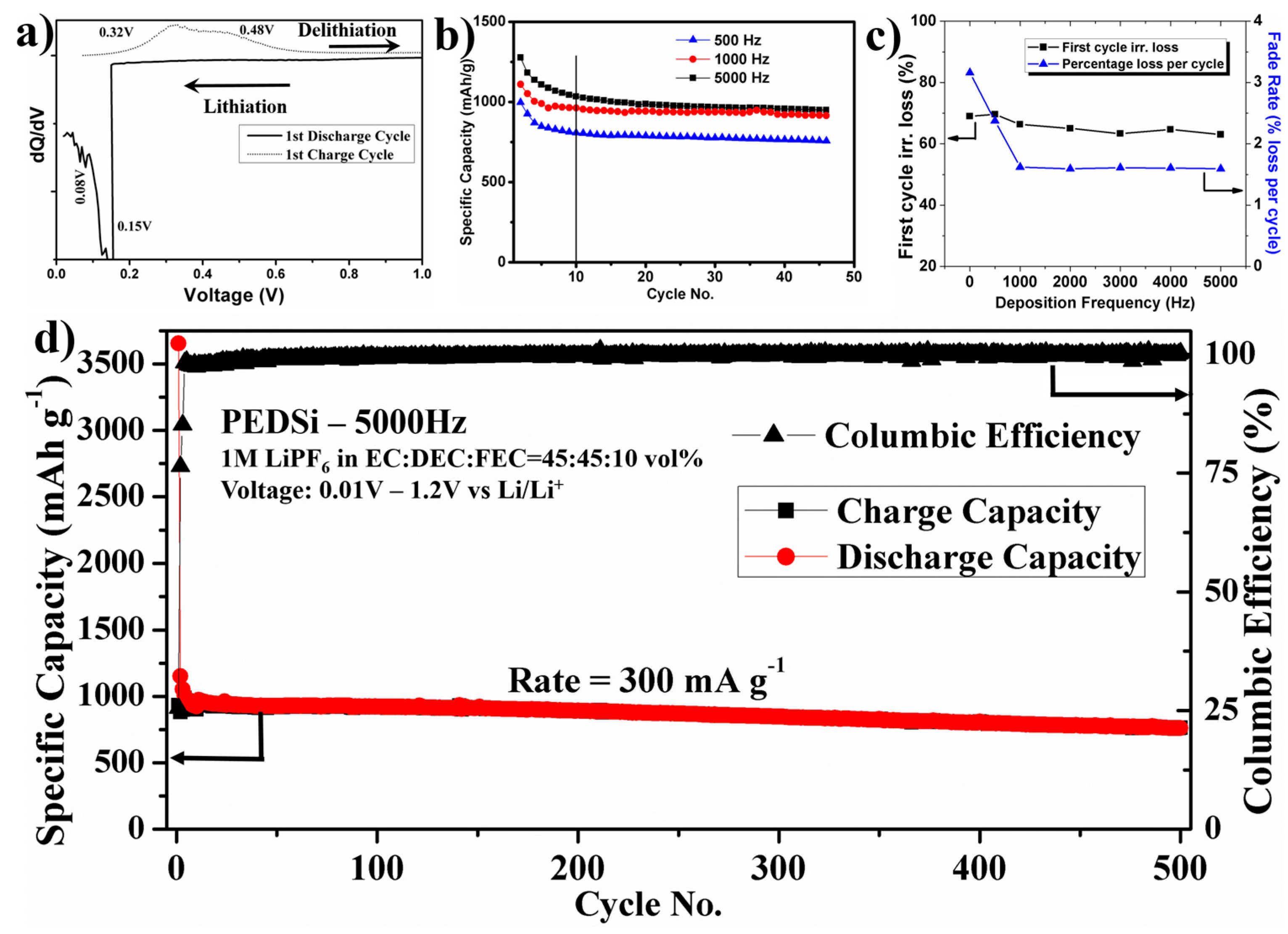
2.3. Electrochemical Characterization of PEDSi on Cu

Electrodeposition driven by controlled atomistic reduction of Si4+ ions, results in direct growth of a-Si thin film on the Cu surface instead of generating discrete loose particles leading to good mechanical and electrical contact at Cu/Si interface due to the likely strong interface adhesion forces. Hence, the pulse electrodeposited Si electrodes were directly assembled in a 2025 coin cell without addition of any binder or Super P and tested with lithium as counter/reference electrode in the voltage window of 0.01–1.2 V. A significant peak is observed close to ~0.15 V during the first discharge cycle in the differential capacity plot (Figure 3a) indicating the alloying reaction of lithium with a-Si and presence of partially alloyed (a-LiySi) and unalloyed (a-Si) two phase region as reported in the literature [52,53,54]. The presence of a potential peak at ~0.08 V indicates various stages of alloying reactions and complete formation of a-LixSi during the end of the first discharge cycle. The charge cycle shows reaction peaks at ~0.32 V and ~0.48 V corresponding to the extraction of lithium from electrode which is commonly observed for the de-alloying reaction from the amorphous LixSi alloy. The columbic efficiency varied from 94% to 98% from the second to fifth cycle, after which it further improved and remained close to 99.7% for the rest of the cycles.
The electrochemical reduction of Si4+ during electrodeposition is accompanied solvent decomposition and reduction of tetrabutylammonium ion (TBA+) leading to formation of carbon and oxygen in the thin film. To calculate the gravimetric capacity of the deposited silicon films, an efficiency parameter for Si4+ reduction is introduced into the Faraday’s law to calculate the actual number of moles of silicon reduced. An efficiency parameter of 35% efficiency is used in the current work, based on previously reported work using similar electrolyte and deposition conditions [31]. The theoretically calculated areal loading density of Si is ~0.1 mg·cm−2 while the experimentally measured loading density of Si is ~0.24–0.28 mg·cm−2. The additional loading density is expected to arise due to the presence of carbon and oxygen in the thin films formed by the reductive decomposition of the solvent and TBACL.
Figure 3b shows the specific capacity plots of pulse electrodeposited silicon films at different frequencies, when tested in lithium ion battery at a current density of 300 mA·g−1. Discharge capacities of 900–1250 mAh·g−1 were obtained with a first cycle irreversible (FIR) loss of ~60%–70% for these films. Electrodeposited silicon is often associated with high FIR loss due to the formation of Si–O–C films instead of pure silicon and presence of chlorine in the films. This occurs due to the reductive decomposition of the propylene carbonate or TBA+, the local over potential on the surface of the electrolyte leading to localized decomposition, presence of minute traces of water in electrolyte, poor ionic conductivity of the electrolyte, and poor electronic conductivity of electrodeposited Si film. The cycling plot also shows a major loss in capacity during the first 10 cycles after which the specific capacity of the Si thin films stabilizes with lower fade rate.
The pulse current deposited conditions showed very minor reduction in FIR with increase in frequency of deposition (Figure 3c) as compared to higher FIR loss exhibited by films deposited under direct current conditions. However, the fade rate in the first 10 cycles showed significant reduction from ~3.15% loss per cycle for films deposited under DC conditions to ~1.5% loss per cycle for PEDSi-5000 Hz. Upon long term cycling at a current rate of 0.3 A·g−1 (Figure 3d), the PEDSi-5000 Hz thin film showed a gravimetric specific discharge capacity of ~810 mAh·g−1 at the end of 500 cycles with a very low fade rate of ~0.056% capacity loss per cycle.
Post cycled SEM analysis of the films for DC conditions showed retention of the island morphology (or cracked film morphology) after 50 charge–discharge cycles which is consistent with the results reported in previous study [31]. PEDSi-500 Hz showed transformation of morphology to cracked thin film morphology during the initial 10 cycles and no further change in the morphology upon further testing till 50 cycles (Figure 4a–c). Continuous thin films deposited under PEDSi-1000 Hz (Figure 4d–f) and PEDSi-5000 Hz (Figure 4g–i), showed development of cracks during the initial 10 cycles of testing after which the films showed no major change in morphology upon further testing, thus indicating the stability of the films due to the improvement in mechanical properties. Electrodeposition being a controlled method involving atomistic adsorption, diffusion and reduction of ions followed by crystallization of atoms, improves the adhesion of thin film to the Cu substrate contributing to mechanical stability of the films. Hence, the electrodeposited films show better performance and stable cycling as compared to sputtered silicon films which fail due to delamination of the films at the substrate–silicon interface [7,55].
A summary of XPS composition analysis of the Si thin films deposited at different frequencies along with depth profiling (increase in etching time) of the thin film and the calculated FIR loss as per the reversible reaction of Si to form metastable Li3.75Si [56,57] and the irreversible reaction of Li with oxygen to form Li2O as shown in Figure 5 is given below.
3.75   Li +   Si     Li 3.75 Si
4   Li +   O 2     2 Li 2 O
The amount of silicon and the ratio of silicon to oxygen increases with depth profiling. Considering that the electrodeposition was conducted under inert conditions and minimal exposure of the films to ambient atmosphere and following earlier reports [45,46], it is likely that increase in oxygen content in the film is probably due to enhanced decomposition of the electrolyte with increase in the thickness of the electrodeposited film and the time of deposition. A similar trend is observed in the calculated FIR loss arising from lithium irreversibly reacting with oxygen indicating that thinner films would show lower FIR loss as compared to thicker films due to the likely reduction in the oxygen content of the electrodeposited thin films following XPS analysis.
The amount of Si content in the film increases with the increase in the frequency of the pulse electrodeposition due to minimal diffusion into the bulk. However, the oxygen content in the film decreases from PEDSi-0 Hz to PEDSi-500 Hz and then increases from PEDSi-500 Hz to PEDSi-5000 Hz. As explained previously at lower frequencies, the growth of Si thin films is guided by relative timescales available for diffusion and reduction of Si4+ ions [47,48]. Due to the enhanced diffusion of Si4+ ions during the OFF TIME the Si content increases and the oxygen content decreases from PEDSi-0 Hz to PEDSi-500 Hz. However, at higher frequencies the deposition is governed by enhanced nucleation combined with electrolyte decomposition with limited growth rate [49,50,51] due to which the content of both silicon and oxygen increases from PEDSi-500 Hz and PEDSi-5000 Hz.
The calculated FIR loss from the XPS composition shows lower FIR loss for PEDSi-500 Hz and PEDSi-5000 Hz when compared to PEDSi-0Hz and PEDSi-1000 Hz. The general drop in the FIR loss with depth is to be expected with the reduction in the surface oxygen in line with Figure 5b. Further, the calculated FIR loss is in the range of 28%–37% for the pulse electrodeposited films while the experimentally observed values are in the range of 60%–70%. The deviation of calculated FIR loss (from XPS compositional analysis) from that observed in electrochemical testing indicates that the FIR loss in these thin films is a combined effect of the loss of lithium due to the oxygen content in the film primarily arising due to electrolyte decomposition and the initial frequency independent disintegration of the thin film during the first cycle discharge. The post-cycled SEM study (Figure 4) which shows change in morphology of thin films during the first 10 cycles also confirms the contribution of material loss due to morphological/microstructural disintegration contributing to the FIR loss. More work is clearly warranted to unequivocally ascertain these inferences. The results nevertheless show the influence of frequency of pulsed current electrodeposition on the evolution of morphology and composition (Si, O, C) of the a-Si thin films with their subsequent influence on the electrochemical cycling response. Further studies could likely lead to improvements in obtaining high capacity as well as lowering the FIR with improved cycling stability, further attesting to the promise of electrodeposition as a viable approach for generating large scale silicon electrodes for lithium-ion applications.

3. Materials and Methods

3.1. Pulse Electrodeposition of Silicon on Cu Substrates

Propylene carbonate (PC, 99.9% anhydrous), tetrabutylammonium chloride (TBACL, >97%), silicon tetrachloride (SiCl4, 99.99%), and acetone (99.9%, anhydrous) used for deposition studies were purchased from Sigma–Aldrich (St. Louis, MO, USA) and were used without further purification. Propylene carbonate was selected as the solvent due to its high dielectric constant (k = 64) which makes it a good medium for dissolving silicon tetrachloride. For the supporting electrolyte, tetrabutylammonium chloride (TBACL, >97%) was dried overnight in vacuum and added to propylene carbonate to improve the conductivity of the electrolyte.
A solution of 0.5 M SiCl4 and 0.1 M TBACL prepared by dissolving 1.12 g TBACL and 2.3 mL SiCl4 in 37.7 mL PC under regulated atmosphere (O2 < 0.1 ppm and H2O < 0.1 ppm) in a glove box was used as the electrolyte for the PED. EC epsilon (Bioanalytical system, West Lafayette, IN, USA) was used to conduct linear sweep voltammetry (LSV) of the electrolyte in a cylindrical three electrode cell made of glass and sealed with teflon gaskets at both the ends. For the pulsed electrodeposition study, bare Cu foil was used as the working electrode while platinum wire (diameter = 0.5 mm, 99.95%, Alfa Aesar, Tewksbury, MA, USA, 1 mm distance from working electrode) and platinum foil (0.5 cm L × 0.5 cm B × 0.1 mm thick, 99.9%, Aldrich, St. Louis, MO, USA) served as the reference and counter electrodes, respectively.
Dynatronix pulse power supply (Dynatronix, Amery, WI, USA) was used for the pulsed current electrodeposition of Si films under an argon atmosphere by converting the three-electrode cell into a two electrode cell. The Cu electrodes were sonicated in ethanol and acetone for 5 min and dried in air before use and 20 ml of the above electrolyte solution was used for the deposition immediately after preparation. The peak current density of the pulsing cycle was 1 mA·cm−2 with a duty cycle of 50%, total charge density of 60 mA-min·cm−2 and the frequency of the cycle was maintained at 0 (galvanostatic), 500, 1000, 2000, 3000, 4000, and 5000 Hz. To remove any traces of electrolyte, salts, and impurities, the copper foils electrodeposited with silicon were first rinsed in PC followed by anhydrous acetone under an argon atmosphere. The foils were then allowed to dry in an argon filled glove box approximately for 1 h before further characterization.

3.2. Material and Electrochemical Characterization

The pulse electrodeposited samples were always sealed in the glove box under an argon atmosphere before transferring them out of the glove box for further studies. Scanning electron microscopy (SEM, Philips XL 30, FEI, Hillsboro, OR, USA) was used to study the morphological characteristics of the thin films and subsequently, attached Energy Dispersive X-ray Spectroscopy (EDAX, AMETEK, Mahwah, NJ, USA) operated at 10 kV was used along with the GENESIS software for conducting qualitative compositional analysis [58]. Raman spectroscopy was performed using a Renishaw inVia Raman microscope (Renishaw, Gloucestershire, UK) equipped with a 633 nm red laser to evaluate the vibrational and rotational modes of the deposited films. PANalytical Empyrean XRD diffractometer (PANalytical, Almelo, Netherlands) was used for performing Glancing angle X-ray diffraction (GAXRD) on the electrodeposited Si thin films. The Cu foil electrodeposited with Si were assembled under argon atmosphere in a half cell (2025 coin cell) using lithium foil as the counter electrode and 1M LiPF6 in ethylene carbonate (EC), diethylene carbonate (DEC), and fluoroethylene carbonate (FEC) with EC:DEC:FEC = 45:45:10 by volume as electrolyte. The assembled coin cell was tested in the potential window of 0.01–1.2 V with respect to Li/Li+, at a current rate of 0.3 A·g−1 to study their performance as anode material.

4. Conclusions

Morphology of amorphous silicon was modified by using frequency-dependent pulse current electrodeposition technique. Under galvanostatic conditions, films show mud crack morphology; while at higher frequencies (>1000 Hz) growth of thin continuous film due to the coalescence of electrodeposited particles is observed. Films electrodeposited at 500 Hz show islands of micron size particles forming discontinuous or continuous films under pulse current conditions decreasing in size with increase in frequency. Difference in the morphology is likely due to change in the nucleation and growth mechanisms of thin films formed at the different frequencies studied. The films show an improvement in performance when tested in LIBs with the increase in frequency due to enhanced stability under pulsed current electrodeposition conditions. Consequently, the fade rate (% loss per cycle) reduced from ~3.15% under DC electrodeposition to ~1.6% for pulsed current frequencies greater than 1000 Hz. The films also showed a major change in morphology during the first 10 cycles of electrochemical testing which supports the high fade rate during initial electrochemical cycling. There was minor reduction in first cycle irreversible (FIR) loss with frequency and the pulse electrodeposited films showed a capacity of ~1000–1250 mAh·g−1 with a columbic efficiency of ~99.7% at the end of ~47 cycles. Upon long term cycling at a current rate of 0.3 A·g−1, the thin films deposited at a 5000 Hz frequency showed a capacity of ~805 mAh·g−1 at the end of 500 cycles with a fade rate of ~0.056% capacity loss per cycle demonstrating very good stability and effects of frequency. The loss of lithium due to the presence of oxygen and the change in mechanical integrity due to volumetric expansion during the initial discharge–charge cycle is the major reason for the high FIR loss.

Acknowledgements

The authors acknowledge support from the National Energy Technology Laboratory’s Regional University Alliance (NETLRUA), a collaborative initiative of the NETL. This technical effort was performed under the RES Contract DEFE0004000. Financial support of Robert Romanosky is also acknowledged. The authors additionally gratefully acknowledge the financial support of the DOE-BATT program (Contract DE-AC02-05CHl1231), the National Science Foundation (NSF-CBET-0933141 and CBET-1511390) and partial support of the Ford Foundation. The authors also acknowledge the Edward R. Weidlein Chair Professorship funds and the Center for Complex Engineered Multifunctional Materials (CCEMM) for partial support of this research. The authors also acknowledge the travel grant provided by Electrodeposition Division of the Electrochemical Society for presentation (MA201401502) of part of the work at the 225th ECS Meeting held 11–15 May 2014 in Orlando, FL, USA [59].

Author Contributions

Ayyakkannu Manivannan and Prashant N. Kumta devised the original concept. Bharat Gattu, Rigved Epur and Ramalinga Kuruba designed the experiments, synthesized the materials, prepared the electrodes, performed SEM/EDAX/XRD, the electrochemical characterization and analyzed the electrochemical data. Pavithra Murugavel Shanti collected and analyzed the XPS data. Moni Kanchan Datta and Prashanth Hanumantha Jampani made important suggestions in the context of fundamental structural and electrochemical characterization. Bharat Gattu, Prashanth Hanumantha Jampani, Moni Kanchan Datta and Prashant N. Kumta wrote the first draft of the paper; and all authors participated in the manuscript revision. The project is conceived and supervised by Prashant N. Kumta.

Conflicts of Interest

The authors declare no conflict of interest.

References

  1. Tarascon, J.M.; Armand, M. Issues and challenges facing rechargeable lithium batteries. Nature 2001, 414, 359–367. [Google Scholar] [CrossRef] [PubMed]
  2. Tran, T.D.; Feikert, J.H.; Song, X.; Kinoshita, K. Commercial carbonaceous materials as lithium intercalation anodes. J. Empir. Leg. Stud. 1995, 142, 3297–3302. [Google Scholar] [CrossRef]
  3. Winter, M.; Besenhard, J.O.; Spahr, M.E.; Novak, P. Insertion electrode materials for rechargeable lithium batteries. Adv. Mater. 1998, 10, 725–763. [Google Scholar] [CrossRef]
  4. Weydanz, W.J.; Wohlfahrt-Mehrens, M.; Huggins, R.A. A room temperature study of the binary lithium–silicon and the ternary lithium–chromium–silicon system for use in rechargeable lithium batteries. J. Power Source 1999, 81–82, 237–242. [Google Scholar] [CrossRef]
  5. Boukamp, B.A.; Lesh, G.C.; Huggins, R.A. All-solid lithium electrodes with mixed-conductor matrix. J. Empir. Leg. Stud. 1981, 128, 725–729. [Google Scholar] [CrossRef]
  6. Amezawa, K.; Yamamoto, N.; Tomii, Y.; Ito, Y. Single-electrode peltier heats of Li–Si alloy electrodes in LICL-KCL eutectic melt. J. Empir. Leg. Stud. 1998, 145, 1986–1993. [Google Scholar] [CrossRef]
  7. Maranchi, J.P.; Hepp, A.F.; Evans, A.G.; Nuhfer, N.T.; Kumta, P.N. Interfacial properties of the a-Si/Cu: Active–inactive thin-film anode system for lithium-ion batteries. J. Empir. Leg. Stud. 2006, 153, A1246–A1253. [Google Scholar]
  8. Kasavajjula, U.; Wang, C.; Appleby, A.J. Nano- and bulk-silicon-based insertion anodes for lithium-ion secondary cells. J. Power Source 2007, 163, 1003–1039. [Google Scholar] [CrossRef]
  9. Chan, C.K.; Peng, H.; Liu, G.; McIlwrath, K.; Zhang, X.F.; Huggins, R.A.; Cui, Y. High-performance lithium battery anodes using silicon nanowires. Nat. Nanotechnol. 2008, 3, 31–35. [Google Scholar] [CrossRef] [PubMed]
  10. Beaulieu, L.Y.; Eberman, K.W.; Turner, R.L.; Krause, L.J.; Dahn, J.R. Colossal reversible volume changes in lithium alloys. Electrochem. Solid State Lett. 2001, 4, A137–A140. [Google Scholar] [CrossRef]
  11. Hatchard, T.D.; Obrovac, M.N.; Dahn, J.R. A comparison of the reactions of the SiSn, SiAg, and SiZn binary systems with L3i. J. Empir. Leg. Stud. 2006, 153, A282–A287. [Google Scholar] [CrossRef]
  12. Cui, L.-F.; Ruffo, R.; Chan, C.K.; Peng, H.; Cui, Y. Crystalline-amorphous core–shell silicon nanowires for high capacity and high current battery electrodes. Nano Lett. 2009, 9, 491–495. [Google Scholar] [CrossRef] [PubMed]
  13. Fuchsbichler, B.; Stangl, C.; Kren, H.; Uhlig, F.; Koller, S. High capacity graphite–silicon composite anode material for lithium-ion batteries. J. Power Source 2011, 196, 2889–2892. [Google Scholar] [CrossRef]
  14. Ryu, J.H.; Kim, J.W.; Sung, Y.E.; Oh, S.M. Failure modes of silicon powder negative electrode in lithium secondary batteries. Electrochem. Solid State Lett. 2004, 7, A306–A309. [Google Scholar] [CrossRef]
  15. Lackner, J.M.; Waldhauser, W.; Ebner, R.; Lenz, W.; Suess, C.; Jakopic, G.; Leising, G.; Hutter, H. Pulsed laser deposition: A new technique for deposition of amorphous siox thin films. Surf. Coat. Technol. 2003, 163, 300–305. [Google Scholar] [CrossRef]
  16. Ohara, S.; Suzuki, J.J.; Sekine, K.; Takamura, T. Attainment of high rate capability of Si film as the anode of Li-ion batteries. Electrochemistry 2003, 71, 1126–1128. [Google Scholar]
  17. Yasuda, S.; Chikyow, T.; Inoue, S.; Matsuki, N.; Miyazaki, K.; Nishio, S.; Kakihana, M.; Koinuma, H. Pulsed laser deposition of photosensitive a-Si thin films. Appl. Phys. A 1999, 69, S925–S927. [Google Scholar] [CrossRef]
  18. Maranchi, J.P.; Hepp, A.F.; Kumta, P.N. High capacity, reversible silicon thin-film anodes for lithium-ion batteries. Electrochem. Solid State Lett. 2003, 6, A198–A201. [Google Scholar] [CrossRef]
  19. Janai, M.; Allred, D.D.; Booth, D.C.; Seraphin, B.O. Optical properties and structure of amorphous silicon films prepared by CVD. Sol. Energy Mater. 1979, 1, 11–27. [Google Scholar] [CrossRef]
  20. Chaisitsak, S. Fabrication of amorphous silicon nanocones by bias-enhanced microwave plasma CVD. Mater. Sci. Eng. B 2007, 137, 205–209. [Google Scholar] [CrossRef]
  21. Wang, W.; Epur, R.; Kumta, P.N. Vertically aligned silicon/carbon nanotube (vascnt) arrays: Hierarchical anodes for lithium-ion battery. Electrochem. Commun. 2011, 13, 429–432. [Google Scholar] [CrossRef]
  22. Wang, W.; Kumta, P.N. Nanostructured hybrid silicon/carbon nanotube heterostructures: Reversible high-capacity lithium-ion anodes. ACS Nano 2010, 4, 2233–2241. [Google Scholar] [CrossRef] [PubMed]
  23. Chen, X.L.; Gerasopoulos, K.; Guo, J.C.; Brown, A.; Wang, C.S.; Ghodssi, R.; Culver, J.N. A patterned 3D silicon anode fabricated by electrodeposition on a virus-structured current collector. Adv. Funct. Mater. 2011, 21, 380–387. [Google Scholar] [CrossRef]
  24. Gobet, J.; Tannenberger, H. Electrodeposition of silicon from a nonaqueous solvent. J. Empir. Leg. Stud. 1988, 135, 109–112. [Google Scholar] [CrossRef]
  25. Munisamy, T.; Bard, A.J. Electrodeposition of Si from organic solvents and studies related to initial stages of Si growth. Electrochim. Acta 2010, 55, 3797–3803. [Google Scholar] [CrossRef]
  26. Nicholson, J.P. Electrodeposition of silicon from nonaqueous solvents. J. Empir. Leg. Stud. 2005, 152, C795–C802. [Google Scholar] [CrossRef]
  27. Nishimura, Y.; Fukunaka, Y. Electrochemical reduction of silicon chloride in a non-aqueous solvent. Electrochim. Acta 2007, 53, 111–116. [Google Scholar] [CrossRef]
  28. Agrawal, A.K.; Austin, A.E. Electrodeposition of silicon from solutions of silicon halides in aprotic solvents. J. Empir. Leg. Stud. 1981, 128, 2292–2296. [Google Scholar] [CrossRef]
  29. Zein El Abedin, S.; Borissenko, N.; Endres, F. Electrodeposition of nanoscale silicon in a room temperature ionic liquid. Electrochem. Commun. 2004, 6, 510–514. [Google Scholar] [CrossRef]
  30. Schmuck, M.; Balducci, A.; Rupp, B.; Kern, W.; Passerini, S.; Winter, M. Alloying of electrodeposited silicon with lithium—A principal study of applicability as anode material for lithium ion batteries. J. Solid State Electrochem. 2010, 14, 2203–2207. [Google Scholar] [CrossRef]
  31. Epur, R.; Ramanathan, M.; Beck, F.R.; Manivannan, A.; Kumta, P.N. Electrodeposition of amorphous silicon anode for lithium ion batteries. Mater. Sci. Eng. B 2012, 177, 1157–1162. [Google Scholar] [CrossRef]
  32. Sharma, A.; Bhattacharya, S.; Das, S.; Das, K. A study on the effect of pulse electrodeposition parameters on the morphology of pure tin coatings. Metall. Mater. Trans. A 2014, 45, 4610–4622. [Google Scholar] [CrossRef]
  33. Rezaei-Sameti, M.; Nadali, S.; Rajabi, J.; Rakhshi, M. The effects of pulse electrodeposition parameters on morphology, hardness and wear behavior of nano-structure Cr–WC composite coatings. J. Mol. Struct. 2012, 1020, 23–27. [Google Scholar] [CrossRef]
  34. Gummow, R.J.; He, Y. Morphology and preferred orientation of pulse electrodeposited magnesium. J. Empir. Leg. Stud. 2010, 157, E45–E49. [Google Scholar] [CrossRef]
  35. Tury, B. A Study on Pulse Electrodeposition of Ni–Co Alloys: Physical and Electrochemical Characterisation; Ph.D. Thesis, Institute for Material Science and Technology, Budapest, Hungary, 2006. [Google Scholar]
  36. Song, T.; Li, D.Y. Tribological, mechanical and electrochemical properties of nanocrystalline copper deposits produced by pulse electrodeposition. Nanotechnology 2006, 17, 65. [Google Scholar]
  37. Nee, C.C.; Kim, W.; Weil, R. Pulsed electrodeposition of Ni–Mo alloys. J. Empir. Leg. Stud. 1988, 135, 1100–1103. [Google Scholar] [CrossRef]
  38. Boonyongmaneerat, Y.; Saengkiettiyut, K.; Saenapitak, S.; Sangsuk, S. Corrosion behavior of reverse-pulse electrodeposited Zn–Ni alloys in saline environment. J. Mater. Eng. Perform. 2014, 23, 302–307. [Google Scholar] [CrossRef]
  39. Ul-Hamid, A.; Dafalla, H.; Quddus, A.; Saricimen, H.; Al-Hadhrami, L.M. Microstructure and surface mechanical properties of pulse electrodeposited nickel. Appl. Surf. Sci. 2011, 257, 9251–9259. [Google Scholar] [CrossRef]
  40. Parker, J.H.; Feldman, D.W.; Ashkin, M. Raman scattering by silicon and germanium. Phys. Rev. 1967, 155, 712–714. [Google Scholar] [CrossRef]
  41. Smit, C.; van Swaaij, R.A.C.M.M.; Donker, H.; Petit, A.M.H.N.; Kessels, W.M.M.; van de Sanden, M.C.M. Determining the material structure of microcrystalline silicon from raman spectra. J. Appl. Phys. 2003, 94, 3582–3588. [Google Scholar] [CrossRef]
  42. Vink, R.L.C.; Barkema, G.T.; van der Weg, W.F. Raman spectra and structure of amorphous Si. Phys. Rev. B 2001, 63, 115210. [Google Scholar] [CrossRef]
  43. Osaka, T.; Nara, H.; Momma, T.; Yokoshima, T. New Si–O–C composite film anode materials for LIB by electrodeposition. J. Mater. Chem. A 2014, 2, 883–896. [Google Scholar] [CrossRef]
  44. Momma, T.; Aoki, S.; Nara, H.; Yokoshima, T.; Osaka, T. Electrodeposited novel highly durable SiOC composite anode for Li battery above several thousands of cycles. Electrochem. Commun. 2011, 13, 969–972. [Google Scholar] [CrossRef]
  45. Nara, H.; Yokoshima, T.; Momma, T.; Osaka, T. Highly durable SiOC composite anode prepared by electrodeposition for lithium secondary batteries. Energy Environ. Sci. 2012, 5, 6500–6505. [Google Scholar] [CrossRef]
  46. Nara, H.; Yokoshima, T.; Otaki, M.; Momma, T.; Osaka, T. Structural analysis of highly-durable SiOC composite anode prepared by electrodeposition for lithium secondary batteries. Electrochim. Acta 2013, 110, 403–410. [Google Scholar] [CrossRef]
  47. Mayers, M.Z.; Kaminski, J.W.; Miller, T.F. Suppression of dendrite formation via pulse charging in rechargeable lithium metal batteries. J. Phys. Chem. C 2012, 116, 26214–26221. [Google Scholar] [CrossRef]
  48. Choo, R.T.C.; Toguri, J.M.; El-Sherik, A.M.; Erb, U. Mass transfer and electrocrystallization analyses of nanocrystalline nickel production by pulse plating. J. Appl. Electrochem. 1995, 25, 384–403. [Google Scholar] [CrossRef]
  49. Ibl, N. Some theoretical aspects of pulse electrolysis. Surf. Technol. 1980, 10, 81–104. [Google Scholar] [CrossRef]
  50. Richoux, V.; Diliberto, S.; Boulanger, C.; Lecuire, J.M. Pulsed electrodeposition of bismuth telluride films: Influence of pulse parameters over nucleation and morphology. Electrochim. Acta 2007, 52, 3053–3060. [Google Scholar] [CrossRef]
  51. Shanthi, C.; Barathan, S.; Jaiswal, R.; Arunachalam, R.M.; Mohan, S. The effect of pulse parameters in electro deposition of silver alloy. Mater. Lett. 2008, 62, 4519–4521. [Google Scholar] [CrossRef]
  52. Epur, R.; Hanumantha, P.J.; Datta, M.K.; Hong, D.; Gattu, B.; Kumta, P.N. A simple and scalable approach to hollow silicon nanotube (h-SiNT) anode architectures of superior electrochemical stability and reversible capacity. J. Mater. Chem. A 2015, 3, 11117–11129. [Google Scholar] [CrossRef]
  53. Datta, M.K.; Maranchi, J.; Chung, S.J.; Epur, R.; Kadakia, K.; Jampani, P.; Kumta, P.N. Amorphous silicon–carbon based nano-scale thin film anode materials for lithium ion batteries. Electrochim. Acta 2011, 56, 4717–4723. [Google Scholar] [CrossRef]
  54. Epur, R.; Datta, M.K.; Kumta, P.N. Nanoscale engineered electrochemically active silicon–CNT heterostructures-novel anodes for Li-ion application. Electrochim. Acta 2012, 85, 680–684. [Google Scholar] [CrossRef]
  55. Pal, S.; Damle, S.S.; Patel, S.H.; Datta, M.K.; Kumta, P.N.; Maiti, S. Modeling the delamination of amorphous-silicon thin film anode for lithium-ion battery. J. Power Source 2014, 246, 149–159. [Google Scholar] [CrossRef]
  56. Obrovac, M.N.; Christensen, L. Structural changes in silicon anodes during lithium insertion/extraction. Electrochem. Solid State Lett. 2004, 7, A93–A96. [Google Scholar] [CrossRef]
  57. Iwamura, S.; Nishihara, H.; Ono, Y.; Morito, H.; Yamane, H.; Nara, H.; Osaka, T.; Kyotani, T. Li-rich Li–Si alloy as a lithium-containing negative electrode material towards high energy lithium-ion batteries. Sci. Rep. 2015, 5, 8085. [Google Scholar] [CrossRef] [PubMed]
  58. Minakshi, M. Examining manganese dioxide electrode in KOH electrolyte using TEM technique. J. Electroanal. Chem. 2008, 616, 99–106. [Google Scholar] [CrossRef]
  59. Gattu, B.; Epur, R.; Datta, M.K.; Manivannan, A.; Kumta, P.N. Pulse electrodeposition of amorphous Si film anodes for Li–ion battery. In Proceedings of the 225th ECS Meeting, Orlando, FL, USA, 11–15 May 2014. [Google Scholar]
Figure 1. (a) Pictorial representation of the pulse electrodeposition setup; (b) standard input current cycle during pulse electrodeposition; (c) input current cycle for pulse current electrodeposition in the current study; (d) linear sweep voltammogram of electrolyte with and without SiCl4 showing the reduction of Si4+ ion and (e) Raman spectral shift of the pulse current electrodeposited silicon films.
Inorganics 05 00027 g001
Figure 2. (a) Energy dispersive spectra (EDAX) and (b) XRD pattern of pulse current electrodeposited thin films. The inset in Figure 2b shows the smoothened XRD curve between 20° < 2θ < 35°. SEM images of (c) PEDSi-0; (d) PEDSi-500; (e) PEDSi-1000 and (f) PEDSi-5000 Hz.
Inorganics 05 00027 g002
Figure 3. (a) Differential capacity vs. Voltage curves of electrodeposited Si film; (b) specific discharge capacity of electrodeposited thin films under different pulse current conditions (from 2nd cycle); (c) Performance of electrodeposited Si films with frequency of deposition. Fade rate (the percentage loss per cycle for first 10 cycles) and first cycle irreversible vs. frequency of deposition; (d) Long-term cycling plot of PEDSi-5000 Hz tested in Li/Li+ system.
Inorganics 05 00027 g003
Figure 4. SEM images of (a,b,c) PEDSi-500 Hz; (d,e,f) PEDSi-1000Hz and (g,h,i) PEDSi-5000 Hz, before, after 10 and after 50 electrochemical testing cycles in lithium ion battery.
Inorganics 05 00027 g004
Figure 5. Depth profile of (a) silicon; (b) oxygen and (c) carbon obtained from XPS compositional analysis. (d) The first cycle irreversible loss calculated from the composition of silicon and oxygen in the thin films at various depths. Black, red, green and blue lines indicate the data for PEDSi-0 Hz, PEDSi-500 Hz, PEDSi-1000 Hz and PEDSi-5000 Hz, respectively.
Inorganics 05 00027 g005
Table 1. Pulse current electrodeposition parameters used in the study.
Sample IDPeak Current Density (mA/cm2)ON TIME (AB) (ms)OFF TIME (CD) (ms)Duty Cycle (%)Frequency (AB+CD)−1 (Hz)Charge (mA·min/cm2)
PEDSi-01.0010100060
PEDSi-5001.00115050060
PEDSi-10001.000.50.550100060
PEDSi-20001.000.250.2550200060
PEDSi-30001.000.170.1750294160
PEDSi-40001.000.130.1252400060
PEDSi-50001.000.10.150500060

