Article

Novel Method Based on Spin-Coating for the Preparation of 2D and 3D Si-Based Anodes for Lithium Ion Batteries

1
Groupe de Recherche en Matériaux, Microélectronique, Acoustique et Nanotechnologies (GREMAN), Unité Mixte de Recherche (UMR) 7347, Centre National de la Recherche Scientifique (CNRS)/Université François Rabelais de Tours, Institut Universitaire de Technologie (IUT) de Blois, 15 rue de la Chocolaterie, Blois 41000, France
2
Groupe de Recherche en Matériaux, Microélectronique, Acoustique et Nanotechnologies (GREMAN), Unité Mixte de Recherche (UMR) 7347, Centre National de la Recherche Scientifique (CNRS)/Université François Rabelais de Tours, Site STMicroelectronics, 16 rue Pierre et Marie Curie, Tours 37071, France
3
Groupe de Recherches sur L’énergétique des Milieux Ionisés (GREMI), Unité Mixte de Recherche (UMR) 7344, Centre National de la Recherche Scientifique (CNRS)/Université d’Orléans, 14 rue d’Issoudun, Orléans 45067, France
4
Physico-Chimie des Matériaux et des Électrolytes Pour L’ENERGIE (PCM2E), Université François Rabelais de Tours, Parc de Grandmont, Tours 37200, France
*
Authors to whom correspondence should be addressed.
ChemEngineering 2017, 1(1), 5; https://doi.org/10.3390/chemengineering1010005
Submission received: 21 June 2017 / Revised: 21 July 2017 / Accepted: 24 July 2017 / Published: 27 July 2017

Abstract

:
The present study describes a novel strategy for preparing thin Silicon 2D and 3D electrodes for lithium ion batteries by a spin coating method. A homogeneous and stable suspension of Si nanoparticles (SiNPs) was prepared by dispersing the nanoparticles in 1-methyl-2-pyrrolidone (NMP) or in the room temperature ionic liquid 1-butyl-1-methylpyrrolidinium bis(trifluoromethylsulfonyl)imide (Pyr14TFSI). This proposed methodology was successfully employed to prepare 2D and 3D with different aspect ratios electrodes. Both 2D and 3D materials were then used as anode materials. The 2D SiNPs anodes exhibit a high reversible capacity, which is close to 3500 mAh·g−1 at C/10. For a higher discharge rate, the capacity of the 2D anode is considerably improved by dispersing the nanoparticles in Pyr14TFSI instead of NMP solvent. In order to further improve the anode performances, graphene particles were added to the SiNPs suspension. The anodes prepared using this suspension method exhibit relatively low columbic efficiency during the first few cycles (less than 30%) and low reversible capacity (2800 mAh·g−1 at C/10). The 3D SiNPs (NMP) electrode shows a higher intensity during cyclic voltammograms and a better stability under galvanostatic cycling than the 2D SiNPs (NMP) electrode.

1. Introduction

With the increasing need of miroenergy storage devices thanks to the miniaturization of biomedical implants, sensors, or integrated circuits, small size integrated batteries are required. Silicon is considered a promising material to prepare negative electrodes for Li-ion batteries due to its capacity of 3579 mAh·g−1 based on the alloyed form of Li15Si4 at room temperature [1,2]. This value is almost 10 times higher than that of graphite (372 mAh·g−1 for LiC6 [3]). However, Si undergoes a huge volumetric expansion during lithiation and alloying reaction (~280% from Si to Li15Si4) [2]. In recent years, several nano- or micro-structured forms of silicon anodes have been reported and intensively explored to solve the silicon volume expansion/contraction problem during lithium insertion/extraction [3,4,5]. In general, these 3D materials show improved performances and durability due to their particular architectures that enable fast Li ion transport and facile strain relaxation. Three-dimensional structured Si has already been prepared in different studies using etching techniques on silicon wafers. For example, it was widely reported that electrochemical etching of a silicon wafer in HF-based electrolyte allows for the preparation of macro or mesoporous silicon anodes [6,7]. The plasma etching technique can also be used to prepare black Si anodes [8]. Moreover, the preparation and the utilization of 1D nanostructures of Si (nanowire or nanotube) as anode materials in lithium batteries have been also reported [9,10,11,12]. Due to its nanoscale dimensions, nanoparticles are more resistant to fractures than bulk particles. Liu et al. [2] report the lithiation behavior of spherical Si nanoparticles and show that a critical size of about 150 nm exists below which cracking does not occur. By keeping in mind the four-fold volume expansion from pure Si to alloyed LixSi, each anode has been designed to allow the LixSi to fill the volume of the electrode space (i.e., the initial Si material occupied originally a quarter of the layer in volume). Furthermore, one can see that the nanostructured Si can provide sufficient intermediate space to withstand large volume expansion during the lithiation reaction. Based on this viewpoint, we are focusing herein on Si anodes prepared by the deposition of Si nanoparticles (SiNPs) on a 2D and 3D silicon substrate using a spin coating technique. This approach can be considered original since very few authors have reported on the deposition of SiNPs using the spin-coating method to date. For example, Zhou et al. [13] showed the possibility of forming a Si/graphene film on a Cu foil using this technique. However, Si anodes based on Si nanoparticles and their composites with carbonaceous materials (e.g., graphene) have already been prepared using more traditional approaches, such as aerosol methods [14,15], freeze-drying [16], sonication followed by vacuum-filtration [17], mechanical blending [18], or low pressure chemical vapor deposition (LPCVD) [15].
In the present study, we adopted the spin coating deposition to design SiNPs based anodes mainly because this technique is cost effective, relatively simple, and fast. The main goal of this study is to demonstrate the possibility of using the spin coating technique to prepare Si based 2D and 3D anodes. For this reason, the morphology and the chemical composition of the homemade Si active layer are presented along with the electrochemical performances of prepared anodes to demonstrate their high gravimetric capacity, coulombic efficiency, and cyclability. Beyond this, during this work, we also highlight that the performances and the durability of these anodes could be drastically improved by incorporating graphene particles in the Si layer or by the deposition of the Si layer from a dispersion of the Si nanoparticles in a room temperature ionic liquid (RTIL).

2. Materials and Methods

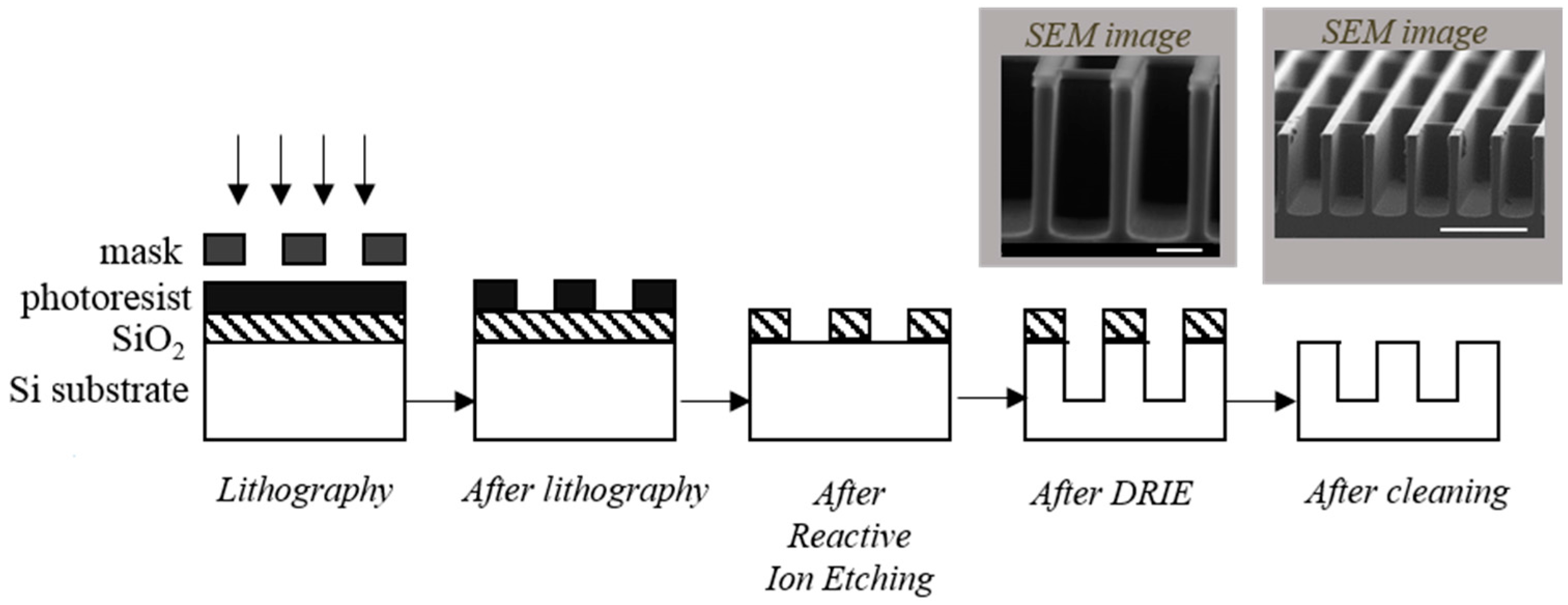
2.1. Preparation of 3D Substrate Materials

A 150 mm diameter, p-type, (100) silicon wafer (Sil’tronix®, Archamps, France) with a thickness of 600–650 µm was used in our experiments with an electrical resistivity of 1–50 Ω·cm.
The standard photolithography technique is performed as indicated in Figure 1. SiO2 thermal oxide is formed on this wafer surface. The positive photoresist (OIR 906-12, Fujifilm®, Washington, DC, USA) was further deposited on the silicon wafer with a 1.2 µm thermal oxide layer using a spin-coater (RC8, Süss MicroTec®, Garching bei München, Germany) to obtain a 1.2 μm thick resist layer, followed by a pre-bake process for 1 min at 90 °C. This coated wafer was then ultraviolet (UV) exposed for 9 s (55 mJ/cm2) using a mask aligner (Süss MicroTec® MA1006), followed by a soft bake for 1 min at 110 °C. The mask plate with 16 cells was designed, and each cell covered area of 3 cm2 and contained uniformly distributed trenches, pores, etc. The sample was then developed in OPD 4280 developer solution for 60 s, followed by rinsing with deionized (DI) water, dried under the flow of nitrogen (N2) gas, and baked at 180 °C. To create openings in the upper SiO2 layer, the silicon substrates were etched by a reactive ion etching (RIE-ICP 200IL, Corial®, Bernin, France) process. During this dry etching, the photoresist residue served as a protective mask. The first step used CHF3 (flow of 30 sccm (standard cubic centimeters per minute)) and C2H4 (3 sccm) mixture for 4 min; this step etched through most of the SiO2 layer and stripped away the photoresist. The second step, another slower etch, cleaned off any residue.
After this etching step, the deep etching by cryogenic process was performed in an inductively coupled plasma reactor (Alcatel Micro Machining Systems®, Paris, France). The protocol for sample preparation and further deep reactive ion etching (DRIE) by cryogenic process experiment has already been described by Tillocher et al. [19,20,21]. The etching conditions for our samples are reported in Table 1. The aspect ratio was the trench depth divided by the trench width. Process gases, SF6 (flow of 200 sccm) and O2 (13 sccm) was injected. The temperature of silicon substrates was controlled from −104 °C to −100 °C by means of a liquid nitrogen circulation and a heating element. Process time varied from 180 to 450 s, depending on the depth of trenches and pores desired (from 15 to 40 µm).
In order to eliminate SiO2 residues, these substrates were washed in an aqueous fluoride solution (40% hydrofluoric acid) for 1–2 min.

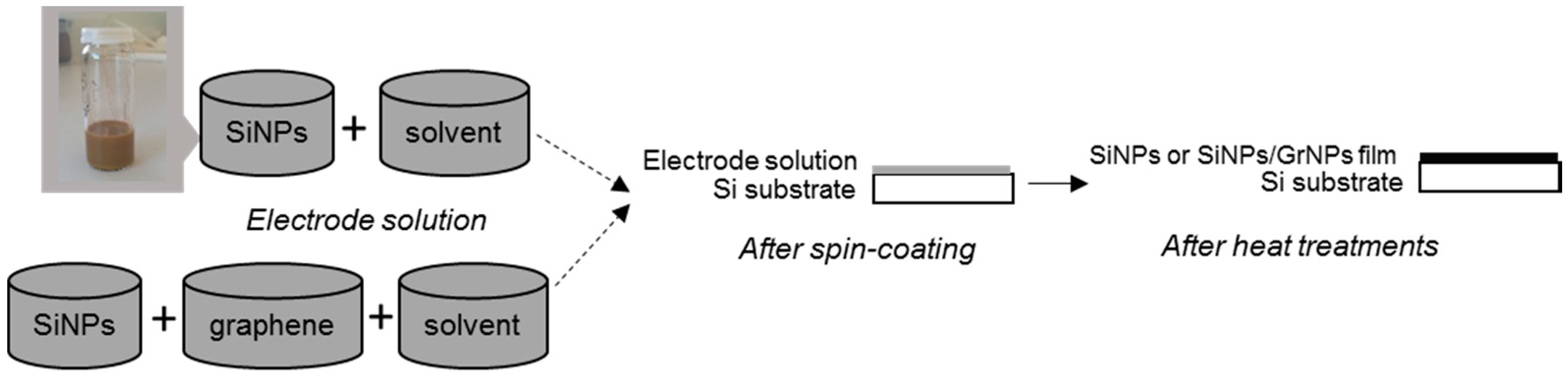
2.2. Electrodes Preparation and Coating Deposition

The thin silicon nanoparticles or SiNPs/GrPNs composites layers were deposited by spin coating method (Figure 2). Silicon nanoparticles powder (Sigma Aldrich®, Saint-Louis, MI, USA, <100 nm) and graphene nanoplatelets powder (Strem Chemical®, Newburyport, MA, USA, 750 m2·g−1) were used as raw materials, and 1-methyl-2-pyrrolidone (NMP, Sigma Aldrich®, purity: 99%) or the RTIL 1-butyl-1-methylpyrrolidinium bis(trifluoromethanesulfonyl)imide (Pyr14TFSI, Solvionic®, Toulouse, France, purity: 99.9%) was used as the solvent. A previous report [22] demonstrated that graphene oxide shows homogenous and stable dispersion in NMP after sonication. One main difference between the NMP and the selected RTIL is that the Pyr14TFSI has a relatively high viscosity (~85 cP [23]). Furthermore, it is well known that this particular RTIL has previously been investigated as a potential alternative electrolyte for Li-ion batteries [24].
Herein, the Si powder was added to the graphene powder by mass to reach a mass ratio close to 4:1 corresponding to 20 wt % of graphene. These powders were dispersed in NMP or Pyr14TFSI (10 g·L−1) at room temperature and homogenized by sonication (Vibracell 75115, Fisher Scientific Bioblock®, Hampton, NY, USA) to obtain a stable suspension. Then, each conformal thin film coating on 3D micro-structured substrate was obtained by following a similar protocol to that described by Vincent et al. [25] by adding a polyester resin (PE-NORSODYNE® S 2010 V, Cray Valley®, Paris, France) to the as-prepared solution with the NMP solvent in a 1.5:1 mass ratio. The above-mentioned process described for the NMP cannot be used for the Pyr14TFSI RTIL solution due to the high viscosity of the RTIL. In this case, with RTIL, the polyester resin is not added. Each resin/dispersion mixture was then deposited on a 1 × 1 cm2 silicon substrate using a spin coater (Spin150, SPS-Europe®, Putten, The Netherlands). This deposition was followed by thermal treatments on hot plates to remove the resin and the solvent. The samples were finally weighed using a Cubis® microbalance (model MSA, Sartorius®, Palaiseau, France) before and after SiNPs deposition allowing the determination of the exact mass of the SiNPs on the substrate.
To ensure good electrical contact during the electrochemical characterizations, a Ti layer (200 nm) was deposited by physical vapor deposition (PVD MP650s, Plassys®, Marolles-en-Hurepoix, France) on the backside of the samples (sputtering rate: 1.7 nm/s, time: ~120 s).

2.3. Characterization

As explained above, in order to remove the solvent and the resin, samples were heated on hot plates after deposit. To set up the appropriate temperature of the heat treatment, thermogravimetric analysis (TGA) analyses of these materials were conducted using diamond thermogravimetry and differential thermal analysis (TG/DTA) (PerkinElmer®, Waltham, MA, USA) equipment under airflow with heating rate of 10 °C/min.
Nanoparticles size distributions were determined by dynamic light scattering (DLS) measurements through the analysis of the effect of the sonication time on the dispersion. These measurements were performed on a NanoZS (Malvern Instruments®, Orsay, France) equipped with a laser source with wavelength of 633 nm at 25 °C. Furthermore, SEM observations were conducted on cross-section samples using a Ultra plus (Zeiss®, Oberkochen, Germany) and a Mira3 microscope (Tescan®, Brno, Czech republic) equipped with an energy dispersive X-ray analysis (EDX) AZtecEnergy set-up from Oxford Instruments® (Abingdon-on-Thames, UK) with a very low accelerating voltage (4–5 kV).
To ensure the graphene presence after thermic cycles in our samples, Raman spectroscopy was used. Raman spectra were obtained by a micro-Raman spectrometer (Renishaw®, Wotton-under-Edge, UK) with a laser source of 514 nm at room temperature.
For electrochemical measurements, half-cells were prepared in an argon-filled glove box within a two electrodes coin cell type battery. The working electrodes were dried Si/SiNPs, and the counter electrodes were lithium foils. These two electrodes were separated with a glass microfiber membrane (GF/C, Whatman®, Maidstone, UK) impregnated with 1 mol·L−1 LiPF6 dissolved in a 1:1:3 mixture of ethylene carbonate (EC, Sigma Aldrich®, purity 99%), propylene carbonate (PC, Sigma Aldrich®, purity 99.7%), and dimethyl carbonate (DMC, Sigma Aldrich®, purity > 99%) by mass. Electrochemical measurements were made with a VMP3 (Bio-Logic Science Instruments®, Seyssinet-Pariset, France). Cyclic voltammograms (CVs) were recorded at a scan rate of 0.025 mV·s−1 between 0.050 and 2 V versus Li/Li+. Galvanostatic charge/discharge cycling was performed under a fixed charge limit and different current. The charge limit value was set to be around 100% of the theoretical capacity (Cth) calculated from Cth (3579 mAh·g−1) and the SiNPs mass determined after the deposition. The potential in charge/discharge processes was limited between 0.05 and 2 V vs. Li/Li+, although the charge was actually terminated with respect to the charge limit rather than the lower potential limit.

3. Results and Discussion

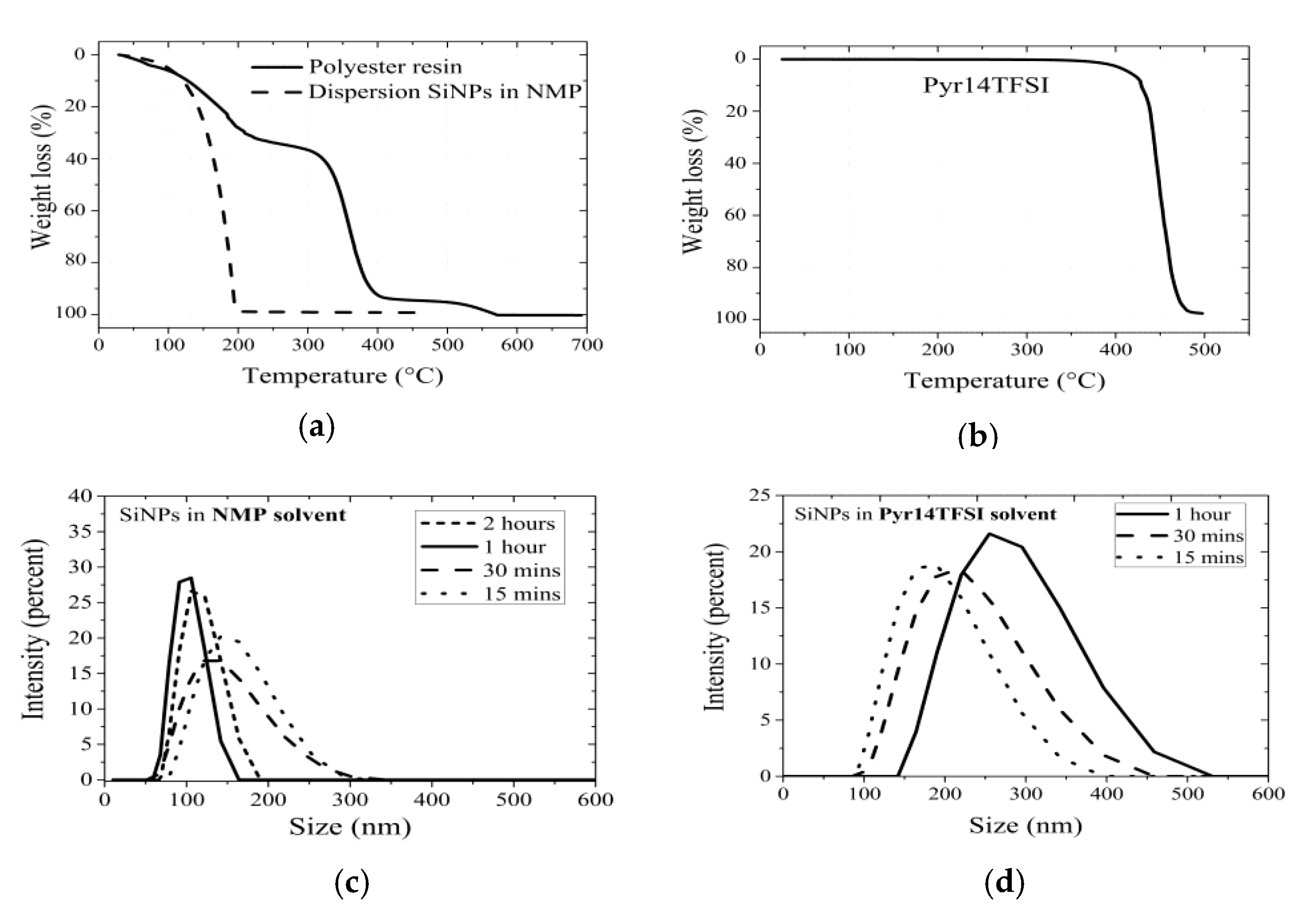
3.1. Thermal Characterization of the Solutions

Figure 3a shows TGA curves for polyester resin and dispersion (SiNPs in NMP) samples recorded at a heating rate of 10 °C·min−1 in airflow. One can see that the NMP solvent can be removed at temperature close to 200 °C. Only Si nanoparticles at a percentage of 1% are present at this temperature (Figure 3a). As shown in Figure 3a, the decomposition of polyester resin is driven by three main reaction stages: the decomposition of the resin terminates at T ≈ 425 °C, with a weight loss close to 94%; the degradation products of the resin are mainly solid carbon, and CO and CO2 under gas form; and the resin/dispersion mixtures are deposited on a 1 × 1 cm2 2D and 3D silicon substrate using a spin coater operated at 5000 rpm for 25 s. After one coating, the sample was kept at room temperature for 1 h, allowing the resin polymerization. Then, it was sequentially heated at 80 °C for 10 min, at 175 °C for 10 min, and at 425 °C for 20 min on a hot plate in order to evaporate the solvent and decompose the polyester resin. This process allowed good adhesion between deposited SiNPs and the substrate current collector. This step is repeated seven times to form the SiNPs thick layer.
Figure 3b shows the TGA trace of the Pyr14TFSI RTIL sample recorded at a heating rate of 10 °C·min−1 in airflow. At around 450 °C, this RTIL starts its decomposition with a weight loss close to 70%. For the process, the sample was heated at this temperature for 5 min to allow the RTIL decomposition. Then, the dispersion mixture (SiNPs or SiNPs/GrNPs in Pyr14TFSI) was deposited by spin coating (at 5000 rpm for 25 s) on a silicon substrate.

3.2. Analysis of the Solutions by DLS

Nanoparticles distributions were determined through the analysis of the solutions by DLS measurements.
Figure 3c shows the particle size distributions in NMP solvent. The absence of particle aggregates confirms the good stability of the obtained dispersions and the narrow distribution of the NPs. From these measurements, the position of the peaks are centered on (155, 140, 105, and 123) nm after (15, 30, 60, and 120) min of sonication, respectively. In fact, DLS results confirm that the ultrasounds allow for the scattering of particles. However, after 2 h of sonication, the particles seem to re-agglomerate together. This explains the increase of the diameter of solvated particles observed. According to our results, the lowest main particles diameter was obtained after 1 h, leading us to select this as the optimal time for the following experiments.
For the Pyr14TFSI-based suspensions (Figure 3d), one can see that the particle size distributions are larger than for NMP solutions (Figure 3c), which could be related to the larger solvation sphere of the Pyr14TFSI than NMP solvent in solution. For example, the position of the observed peak is centered on (196, 226, and 285) nm after (15, 30, and 60) min of sonication, respectively. This leads to a lower main particles diameter value obtained after 15 min, which seems to be much quicker than with the NMP solvent.

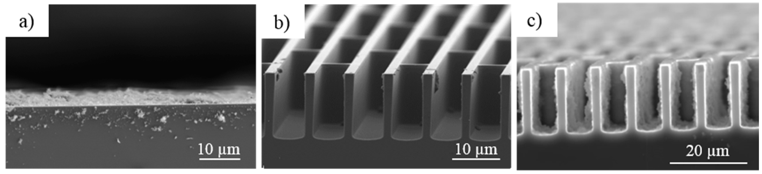
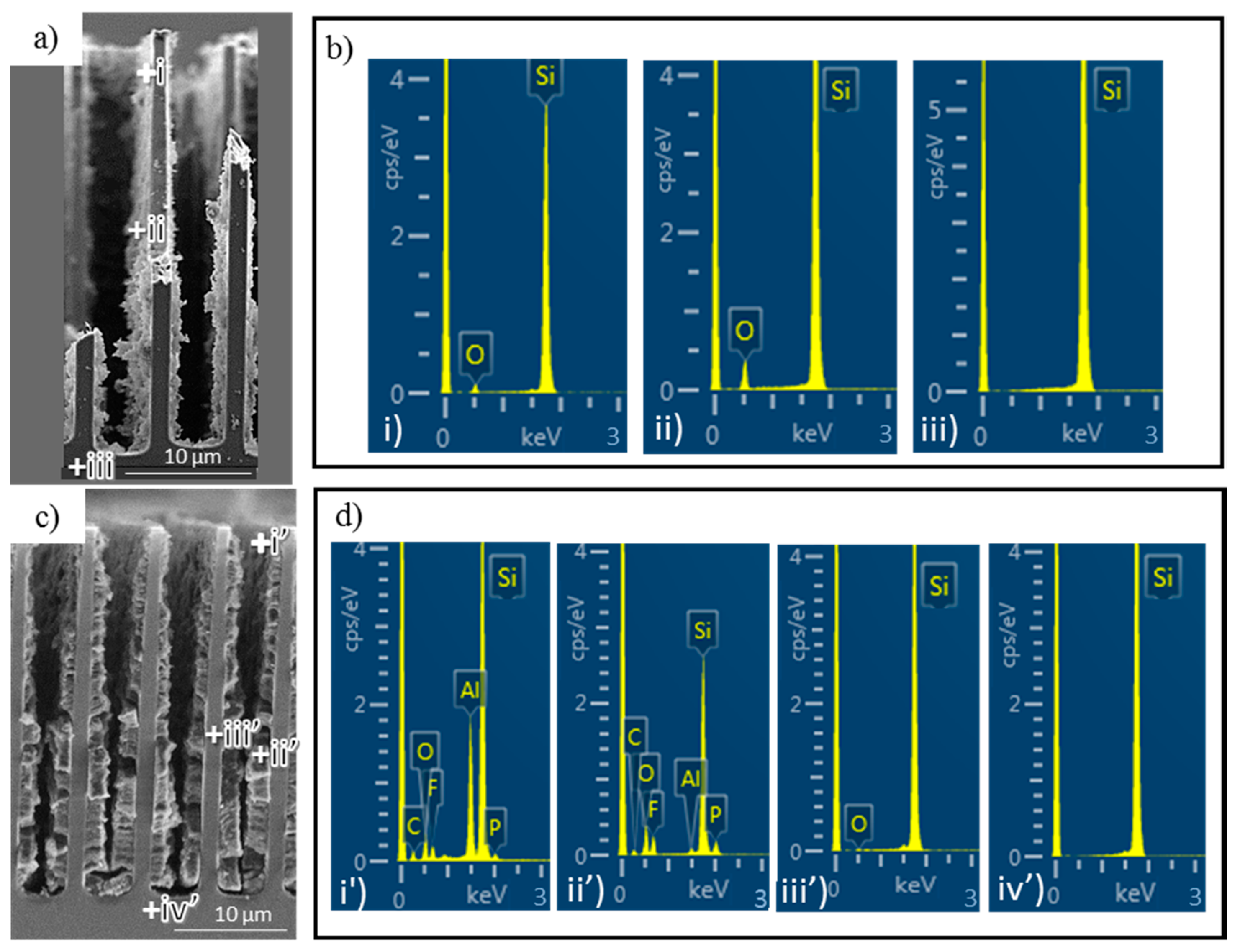
3.3. Morphological Analysis of the 2D and 3D Electrodes

Figure 4a shows the SEM image of 2D electrode after SiNPs deposition with NMP solvent. The coating process described on the experimental part was repeated seven times in order to form a layer of 2.46 µm. The procedure of deposit did not change the morphology and the size of nanoparticles, which remain accessible to the electrolyte. However, some pieces observed on the Si substrate on the SEM image of this SiNPs (NMP) electrode could be explained by the cleavage of our sample when preparing the SEM experiment.
Figure 4b shows SEM images of silicon trenches with an aspect ratio of 3 after etching and cleaning, without the SiO2 layer of 1.2 µm. For the same sample, Figure 4c depicts SEM image after layers deposition. The surface area enlargement depends on the trenches width, trenches depth and spacing between these structures. Here, the trenches with an aspect ratio of 7 are deeper (35 µm) than the trenches with a lower aspect ratio of 3 (Figure 4b, 17 µm) for a same opening (5 µm). As a result and based on the formula defined in the literature [26], for trenches with an aspect ratio of 3 and of 7, a footprint area of 1 cm2 is developed into 5 and 13 cm2 of useful surface area, respectively. The cross-sectional views after SiNPs deposition (Figure 4c) show that the SiNPs can penetrate inside the trenches and cover the walls. The same process as done for the 2D electrode using NMP solvent, presented in the experimental section and repeated seven times, was used for the 3D electrodes. This allows us to design a thickness of the SiNPs deposited on the bottom of Si 3D DRIE etched substrate close to 800 nm.

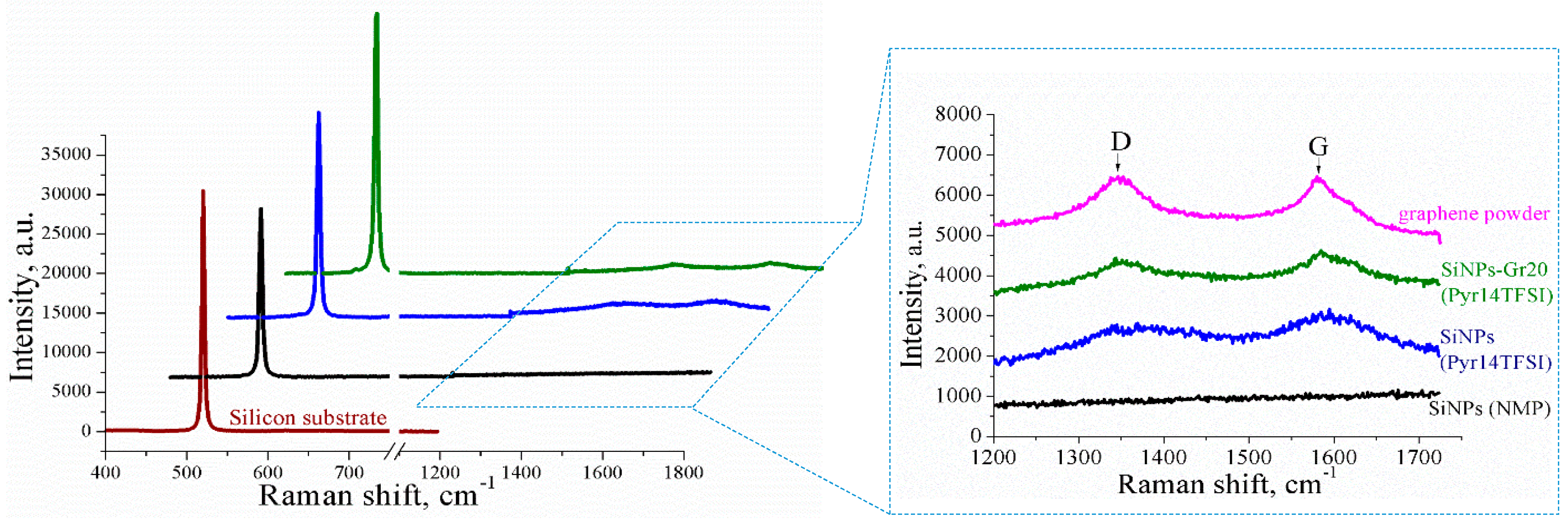
3.4. Raman Characterizations of the Layers

Figure 5 shows the Raman spectra of silicon substrate, graphene powder, Si/SiNPs-Gr20 (solvent Pyr14TFSI with 20 wt %. of graphene), Si/SiNPs (Pyr14TFSI), and Si/SiNPs (NMP) electrodes. The peak observed at 520 cm−1 is characteristic of a highly crystalline Si. As attested by the focus on the 1200–1750 cm−1 range in the Figure 5, the spectra display the carbon D and G band peaks at around 1350 and 1580 cm−1, respectively. These results are consistent with previous studies [27,28,29,30]. The G-band is characteristic of graphitic sheets, and the D-band is attributed to the presence of defects in the hexagonal graphitic structure. Raman analysis of Si/SiNPs-Gr20 (Pyr14TFSI) layers clearly indicates that graphene has been successfully introduced into the Si layer. The G and D bands are not visible in the case of Si/SiNPs (NMP) layer, whereas Raman spectra of Si/SiNPs (Pyr14TFSI) and Si/SiNPs-Gr20 (Pyr14TFSI) electrodes present two large bands at the same frequencies as those for the D and G bands. This may be due to the Pyr14TFSI decomposition during the heating treatment of the layer after deposition, which leads to the formation of amorphous carbon.
Data presented so far show that the proposed spin-coating-based method seems to be suitable for preparing 2D/3D electrode materials. However, does this method affect the electrochemical properties of these 2D and 3D electrodes?

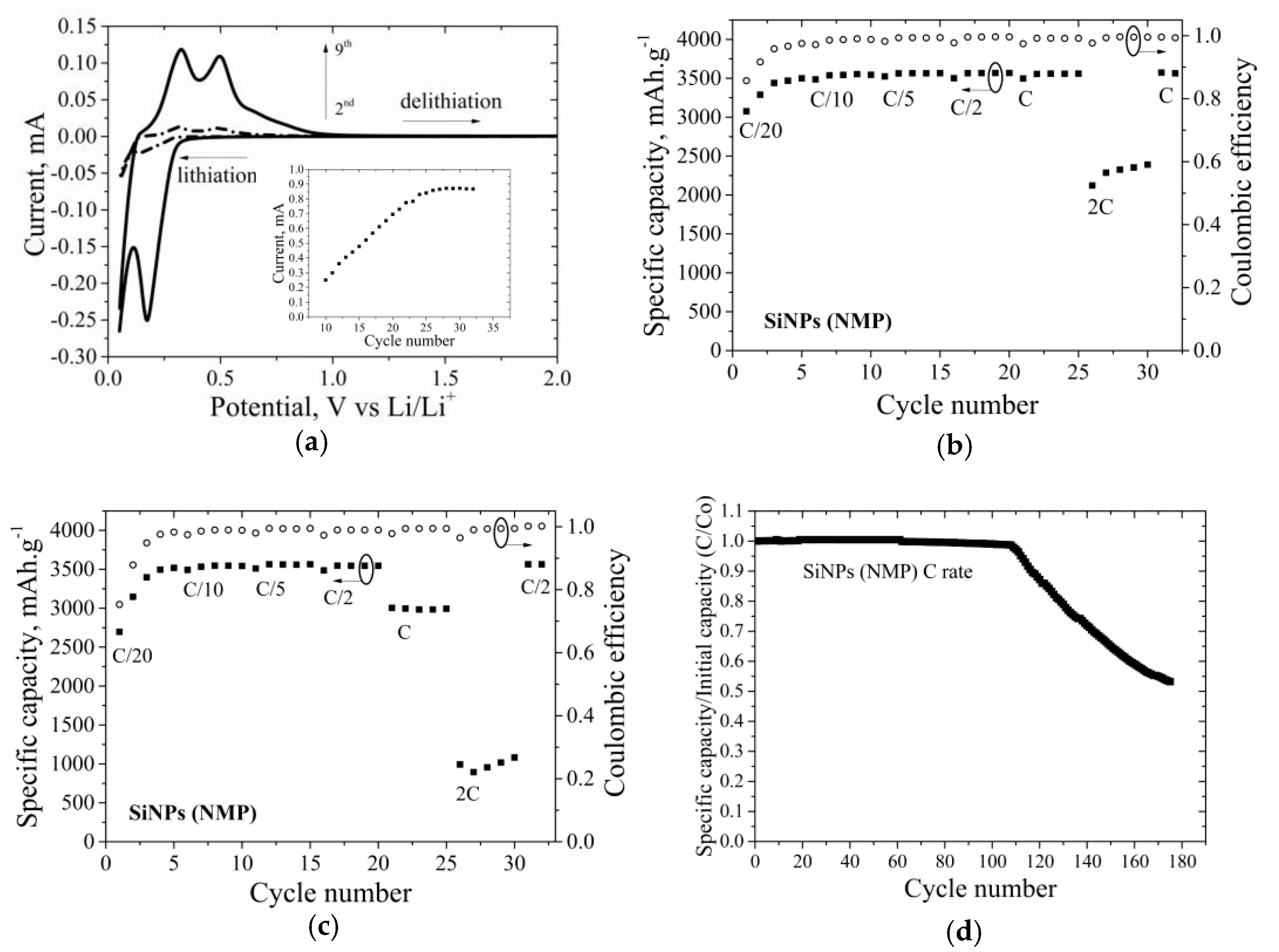
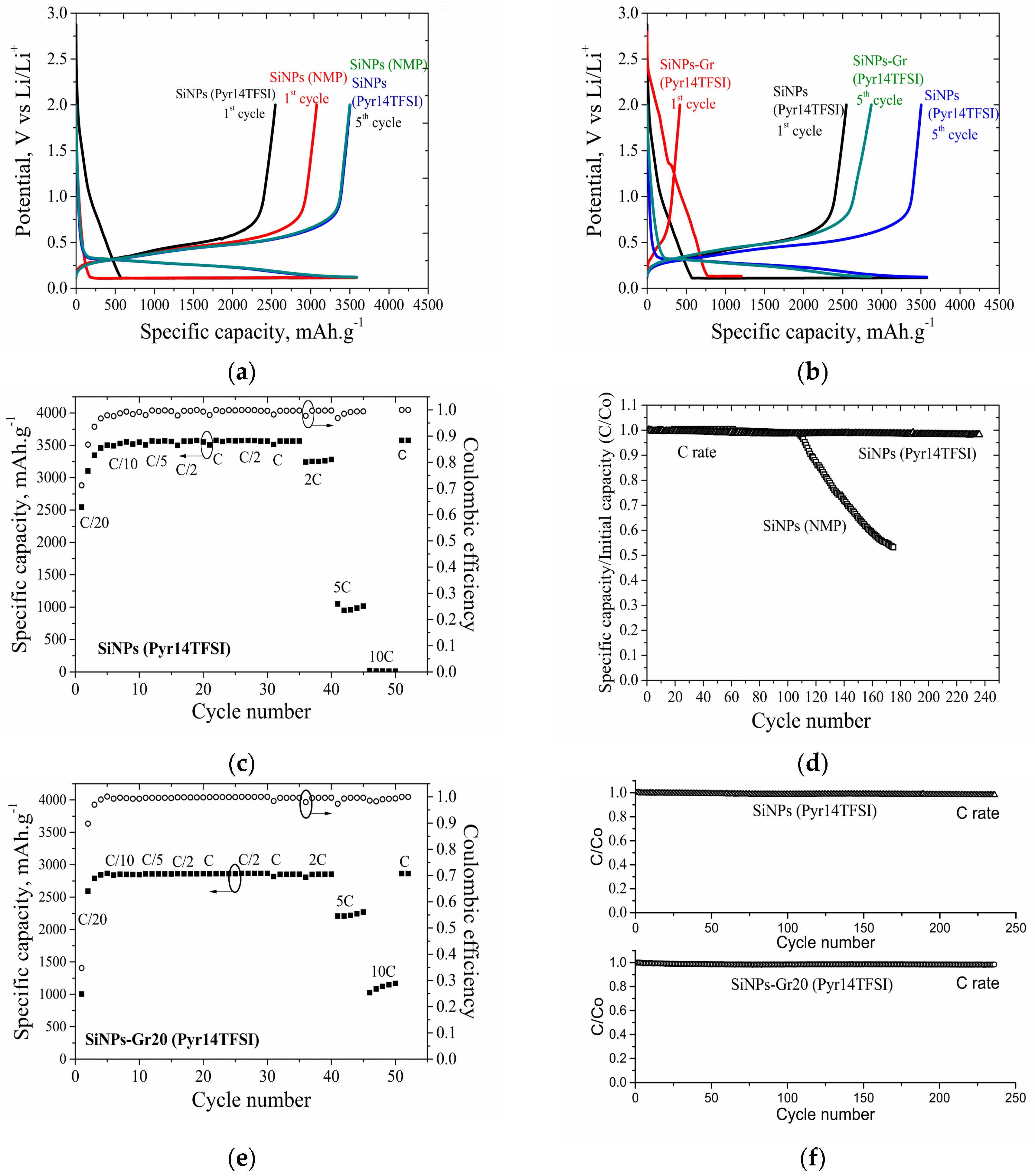
3.5. Electrochemical Properties of the 2D and 3D Electrodes

3.5.1. 2D Electrodes

Figure 6a shows CVs performed using an electrolyte based on the EC:PC:3DMC containing 1 mol·L−1 LiPF6 and recorded at the second and ninth scans using the 2D SiNPs (NMP) electrode. A clear difference between the second and ninth voltammetry cycles is observed. The current density and hence the charge transferred during lithiation/delithiation process increases with the number of scans. The shape of these cyclic voltammograms are consistent with those reported in many previous studies [26,31,32]. The anodic peaks at potentials of 0.32 and 0.50 V observed during the second cycle are attributed to the delithiation reactions of LixSi phases [6,7,33,34,35]. During lithiation reaction (negative current), the two peaks correspond to the symmetrical reversible process of the two anodic peaks. The lithiation/delithiation process results in internal structural changes of the Si electrodes. The rate of observed activation phenomenon is governed by the transport rate of lithium into crystalline silicon or the rate of amorphous Si-Li alloy formation. This gradual activation occurs at each cycle. This enhancement during cyclic voltammetry of the Si samples could be associated to an increase in the Si amount taking part in the lithiation/delithiation process. Li penetrated deeper into the porous electrode.
During 25 CV cycles, the cathode peak intensities increase (the inset of Figure 6a). This current intensity is stabilized for the following cycle. The attainment of steady state cycling suggests the contribution of a constant quantity of Si in the lithiation process. In view of this result, one cannot exclude a lithiation of the Si substrate. However, one can suppose that a lithiation of the substrate would lead to a loss of contact between the layer of SiNPs and the substrate driving a decrease of the performances and capacity. However, results clearly show that such a decrease does not occur (except for the layer SiNPs using the NMP solvent, Figure 6d). In the light of such result, it can be considered that only Si nanoparticles layers are involved in the lithiation/delithiation reactions.
To investigate this in detail, a layer barrier of Ti (100 nm) was also deposited on a 2D substrate by PVD between the SiNPs (Pyr14TFSI) and the substrate. However, by following this methodology, similar electrochemical behavior and capacity were achieved, proving that only the SiNPs layer is involved during lithiation/delithiation reactions.
Figure 6b,c show galvanostatic cycling at different current rates for two Li/SiNPs (solvent NMP) half-cells. For the 2D SiNPs (NMP) electrode with a lower mass (34 µg·cm−2), at C/20, C/10, C/5, C/2, and C rates, stable capacity is recorded with value close to 3500 mAh·g−1 (Figure 6b). However, a stronger capacity fading is observed at 2 C rate to reach a capacity close to 2140 mAh·g−1. However, this capacity fading starts from a lower C rate when the Si nanoparticles mass loading is increased (60 µg·cm−2). Indeed, the electrode keeps its full initial capacity of 3500 mAh·g−1 until C/2 rate prior to decrease for higher C as shown in Figure 6c. This behavior at the high rate could be related to the fact that Li cannot alloy the Si material in depth. This apparent fading is not due to a loss or degradation of the electrode. This is further exemplified in Figure 6b,c, as the capacity returned to its precedent value at C or C/2 rates for Si electrodes with the lowest or highest tested mass, respectively. As can be seen in Figure 6b,c, the specific capacity decreases by increasing the weight of the active mass (i.e., SiNPs loading). Moreover, this behavior is more marked when increasing the charge/discharge rate. Such observations may be explained by the increase of the diffusion depth of the electrolyte into the active material, which could be an evidence that the obtained capacity is due to the SiNPs layer. During the first cycle of charge and discharge, a lower coulombic efficiency is also observed for SiNPs (NMP) electrode with a higher mass electrode (75%, Figure 6c) compared to the SiNPs (NMP) electrode with lower mass loading (86%, Figure 6b). This could be related to the higher mass loading and a higher surface exposed to the electrolyte resulting to a higher electrolyte reactivity with SiNPs electrode to form the SEI layer (solid-electrolyte interphase).
Figure 6d displays the stability under galvanostatic cycling at 1 C rate for SiNPs (NMP) electrode. During the first cycles, a stable capacity is recorded at 1 C rate; however, a strong and rapid capacity fading is then however observed starting from the 105th charge/discharge cycle. This decrease could be explained by the SEI layer formation [3,4], which results from the decomposition of the electrolyte. The cycle life depends of the SEI stability at the interface between SiNPs and the liquid electrolyte. The large volume change during the lithiation/delithiation process cracks the SEI layer. Thus, SiNPs are exposed to the electrolyte while the SEI film continues to grow. As a consequence, active Si particles can be isolated by the electric-insulated SEI layer and lose electrochemical activity, explaining the observed capacity fading shown in Figure 6d. Another reason could also be related to the conductivity loss of SiNPs, which leads to lithiation more and more in depth until the substrate is reached. The substrate cannot support volume changes and therefore involves some material fractures. To confirm this hypothesis, post-mortem analyses were carried out using SEM to show that the layers were compact and confirm the formation of SEI film. However, no crack of the Si substrate were observed.
Figure 7a shows voltage curves of the SiNPs (NMP) and SiNPs (Pyr14TFSI) electrodes cycled vs. lithium metal between 0.05 and 2 V. The obtained voltage curves are characteristic of Si material [32]. The SiNPs (NMP) and SiNPs (Pyr14TFSI) delivered an initial delithiation capacity of 3060 and 2545 mAh·g−1 at C/20 rate, respectively. These capacities increase for the following cycles. After five cycles at C/20, on deep galvanostatic cycling between 0.05 and 2 V, the delithiation capacity for these two electrodes reached a same value close to 3500 mAh·g−1, which is about 10 times higher than the theoretical capacity of graphite. Rate-capability tests show that SiNPs (NMP and Pyr14TFSI) electrodes retain their stable cycling stability at various rates, as shown in Figure 6b and Figure 7c. As seen from Raman analysis (Figure 5), SiNPs (Pyr14TFSI) electrode contains amorphous carbon. This presence leads to a higher surface exposed to the electrolyte, which could explain the higher electrolyte reactivity with the electrode to form the SEI layer. This could also explain the irreversibility observed for SiNPs (Pyr14TFSI) electrode in the first cycle (Figure 7a) and a smaller coulombic efficiency observed for this electrode (71%, Figure 7c) compared to SiNPs (NMP) electrode (86%, Figure 6b).
Galvanostatic cycling at different current rates for a Li/SiNPs (solvent Pyr14TFSI) half-cell is displayed in Figure 7c. Furthermore, for Li/SiNPs (Figure 7c), a high capacity close to 3500 mAh·g−1 is stable for five cycles even at C/20, C/10, C/5, C/2, and C rates. However, the reversible capacity decreases when current rate increases. For example, at a current density higher than 2 C rate, a strong decrease was then observed to reach a capacity close to 3250 mAh·g−1. However, this apparent fading is not due to a loss nor a degradation of the electrode as similar capacity is observed when measuring its value at a lower rate (i.e., at 1 C rate).
Impact of solvent used (NMP or Pyr14TFSI) on materials could be assessed by comparing Figure 6b and Figure 7c. For electrode SiNPs (NMP solvent, Figure 6b), at C/20, C/10, C/5, C/2, and C rates, stable capacity is recorded with value close to 3500 mAh·g−1. For an applied current rate of 2 C, a strong decrease is observed from 3560 to 2140 mAh·g−1. However, even if this fading at a 2 C rate is also observed for electrode SiNPs (Pyr14TFSI solvent, Figure 7c), it seems to be less important, as the capacity only decreases from 3560 to 3250 mAh·g−1.
For SiNPs (Pyr14TFSI) electrode (Figure 7d), the capacity is stable during 235 cycles at 1 C rate, which could be related to the fact that this electrode contains amorphous carbon, as shown during the Raman analysis (Figure 5). Furthermore, this electrode shows much better cycling stability compared to the SiNPs (NMP) electrode (Figure 6d). This difference could be associated to the carbon coatings on Si electrodes, which have been reported to modify the SEI morphology and exhibited smooth surfaces with limited pore structure [36,37].
Figure 7b shows voltage curves of the SiNPs (Pyr14TFSI) and SiNPs-Gr (Pyr14TFSI) electrodes cycled vs. lithium metal between 0.05 and 2 V. The initial lithiation voltages are 2.87 and 2.79 V for SiNPs (Pyr14TFSI) and SiNPs-Gr (Pr14TFSI) electrodes, respectively. While, the SiNPs (Pyr14TFSI) and SiNPs-Gr (Pyr14TFSI) deliver an initial delithiation capacity of 2545 and 415 mAh·g−1 at C/20 rate, respectively. These capacities increase for the following cycles. For example, after five cycles at C/20, the delithiation capacity for these electrodes reached 3500 and 2857 mAh·g−1 for SiNPs (Pyr14TFSI) and SiNPs-Gr (Pyr14TFSI), respectively. Furthermore, the SiNPs-Gr (Pyr14TFSI) electrode delivers a specific capacity close to 1200 mAh·g−1 in the initial lithiation and a reversible capacity of 415 mAh·g−1 in the first delithiation. The irreversible capacity can be associated with the formation of the SEI layer in the first cycle.
As shown in Figure 7e, the capacity of Li/SiNPs-Gr20 (Pyr14TFSI) cell, recorded with value close to 2860 mAh·g−1, presents a good stability until 2 C rate and decreases for the following current rates. This cell has a better stability than Li/SiNPs (Pyr14TFSI) cell. This is likely due to the improvement of the interfacial conductivities linked to the presence of amorphous carbon and graphene. At 2 C rate, 100% of initial capacity is retained even, and only 22% is lost at 5C rate. However, at 10 C, its capacity reaches a value of 1120 mAh·g−1. The high surface area of graphene (750 m2·g−1) produces a stable cycle performance when the hybrid is used as anode material for Li-ion batteries. In other words, the graphene network accommodates large volume changes of Si nanoparticles [38].
A low initial coulombic efficiency for SiNPs-Gr20 (Pyr14TFSI) (35% versus 70% for SiNPs (Pyr14TFSI)) is observed for the first cycle. This could be related to the high specific surface of the graphene and to a larger surface of the anode material is exposed to the electrolyte. Thus, the formation of the SEI layer is promoted, leading to a more irreversible loss in capacity, and therefore a lower initial coulombic efficiency [39]. This result is consistent with previous study in which electrodes containing graphene with high surface areas exhibit a low coulombic efficiency due to the irreversible formation of a large SEI layer over their entire area [40].
Figure 7f displays galvanostatic profiles for SiNPs (Pyr14TFSI) and SiNPs-Gr20 (Pyr14TFSI) electrode. For SiNPs-Gr20 (Pyr14TFSI) and SiNPs (Pyr14TFSI) electrodes, stable capacity is observed at 1 C rate.

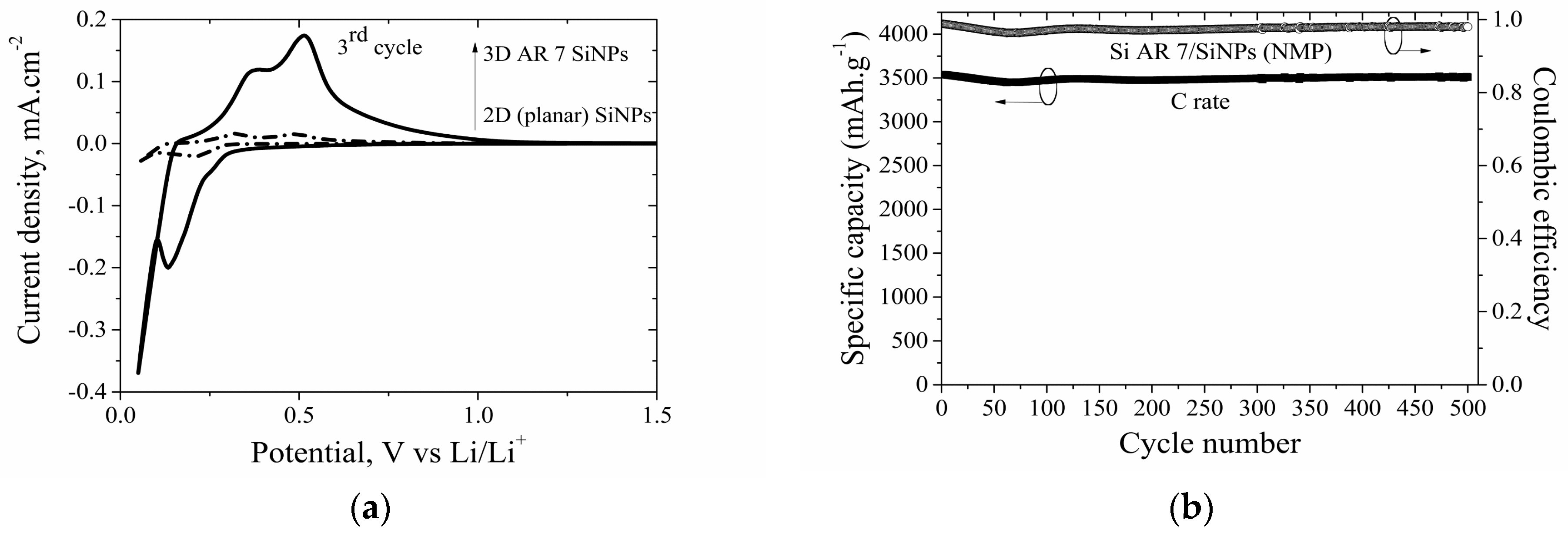
3.5.2. 3D Electrodes

Figure 8a depicts the cyclic voltammograms of 2D and 3D electrodes with trenches with an aspect ratio of 7. The 3D shape electrode with trenches with an aspect ratio of 7 enhances its specific surface area. Thus, the SiNPs layers deposited inside the trenches with specific surface area of 13 cm2 (AR 7) show a larger increase of the current density compared to planar electrode.
Figure 8b shows the stability under galvanostatic cycling at 1 C rate for SiNPs (NMP) coating onto trenches with an aspect ratio of 7. A stable capacity is recorded at 1 C rate with an average value of 3500 mAh·g−1. Contrary to the 2D electrode (see Figure 6d), no fading is observed. In other words, the 3D electrode seems to be more stable, mainly due to its high useful surface area.
The Figure 9a depicts the SEM image of trenches structure with an aspect ratio of 7. The active material mass loading is 43 µg·cm−2. The SiNPs can penetrate inside the trenches and cover the walls. Some breakages observed on the Si substrate on the SEM image of this SiNPs (NMP) electrode could be explained by the cleavage of our sample when preparing the SEM experiment. The data generated by EDX analysis are presented in Figure 9b. Three regions were analyzed: (i) the surface, (ii) the half-height, and (iii) the wafer silicon. The two first spectra show peaks corresponding to the elements Si and O, characteristics of the SiNPs layer. At the wafer silicon, only silicon is observed.
The Figure 9c shows the SEM post-mortem analysis for 3D electrodes after 500 consecutives galvanostatic cycles at 1 C rate. One can see that the layer becomes denser. This phenomenon is consistent with a previous study [41]. As the electrode is still stable electrochemically, the material unsticking is probably due to the cleavage of the sample. The pores kept the same depth and width after lithiation-delithiation cycles. Thus, the Si wafer seems to remain unaffected even after long-time cycling. To confirm this hypothesis, EDX post-mortem analyses were performed on the trenches. The data generated by EDX characterization are represented in Figure 9d. Four regions were analyzed: (i’) the surface, (ii’) the half-height, (iii’) the bulk Si, and (iv’) wafer Silicon. The two first spectra (regions (i’) and (ii’)) show peaks corresponding to the elements Si, O, C, Al, P, and F. The presence of the element Al could be explained by the use of an aluminum SEM cross section holder during SEM observation. The SEI layer is composed of PEO-type oligomers (polyethylene oxide), Li2CO3, LiF, LiPF6, LixPFy, and LixPFyOz products [42,43,44,45]. Thus, in the light of this observation, one can suggest that electrolyte decomposition occurs in the regions where carbon, phosphorous, and fluorine are present. In contrast, at the bulk Si and at the wafer Silicon (regions (iii’) and (iv’)), phosphorous and fluorine are not observed. This observation supports that bulk Si is not involved during lithiation/delithiation process.

4. Conclusions

The aim of this study was to set up a novel approach to deposit SiNPs layer driven by a liquid route with or without graphene nanoplatelets onto a 2D and 3D Si substrate with different aspect ratios using a spin coating technique. This method was selected mainly because it is relatively easily, fast, and cheap, and in fact could be potentially used in industrial applications. Furthermore, during this work, two solvents were used (NMP and Pyr14TFSI) as a proof of concept. The electrochemical properties of layers deposited using NMP or Pyr14TFSI onto the same 2D Si substrate are different. The use of Pyr14TFSI allows amorphous carbon formation into the SiNPs layer, which could be related by its non-volatility and its tendency to decompose rather than evaporate, contrary to conventional solvents such as NMP. For this SiNPs (Pyr14TFSI) electrode, a stable capacity was recorded during 240 cycles at 1 C rate with an average value of 3560 mAh·g−1. With graphene addition, the electrode showed an inferior capacity, close to 2860 mAh·g−1, which was stable during 240 cycles. The retention of the capacity value at high rate is due to the electrical conductivity of graphene which is higher than silicon material. However, the presence of graphene or/and amorphous carbon improves the cycle life of the electrode, which could be due to the increase of the layer conductivity. In this paper, we also showed the increase of the cathodic peak during CV cycling of the 3D electrode with trenches with an aspect ratio of 7 by a factor of about 13, compared to planar electrode, due to its higher specific surface area (13 cm2 for AR 7). Thus, only the SiNPs or SiNPs/GrNPs layer is involved in the lithiation and delithiation reactions, while Si bulk remained unaffected even after long-time cycling. Finally, this work also demonstrates that SiNPs or SiNPs/GrNPs composite obtained by this novel method could be used as negative material for Li-ion batteries.

Acknowledgments

The authors would like to thank Pierre-Yvan Raynal (PPF ASB Tours) for performing SEM observations and Katel Herve Aubert (NMNS Tours) for performing the DLS analysis. The authors are also grateful to the STOCKE-DEPOYDE project supported by the Région Centre, France, for its financial support.

Author Contributions

Marie Gabard prepared the electrode solutions, performed the deposition, the DRIE experiments, the characterizations (TGA, SEM, EDX and electrochemical measurements), analyzed TGA, DLS, SEM, EDX and the electrochemical data and wrote the paper. Mustapha Zaghrioui performed the Raman experiments and analyzed the data. David Chouteau and Virginie Grimal performed the lithography and the RIE experiments, respectively and the data analysis. Thomas Tillocher supervised the DRIE experiments and the data analysis. Fouad Ghamouss supervised the electrochemical studies on the Si anode, the data analysis and contributed in the paper writing. Nathalie Poirot supervised the electrode preparation and the deposition by spin-coating method, the data analysis and provided feedback on drafts of the paper.

Conflicts of Interest

The authors declare no conflict of interest.

References

  1. Kasavajjula, U.; Wang, C.; Appleby, A.J. Nano- and bulk-silicon-based insertion anodes for lithium-ion secondary cells. J. Power Sources 2007, 163, 1003–1039. [Google Scholar] [CrossRef]
  2. Liu, X.H.; Zhong, L.; Huang, S.; Mao, S.X.; Zhu, T.; Huang, J.Y. Size-dependent fracture of silicon nanoparticles during lithiation. ACS Nano 2012, 6, 1522–1531. [Google Scholar] [CrossRef] [PubMed]
  3. Liang, B.; Liu, Y.; Xu, Y. Silicon-based materials as high capacity anodes for next generation lithium ion batteries. J. Power Sources 2014, 267, 469–490. [Google Scholar] [CrossRef]
  4. Su, X.; Wu, Q.; Li, J.; Xiao, X.; Lott, A.; Lu, W.; Sheldon, B.W.; Wu, J. Silicon-based nanomaterials for lithium-ion batteries: A review. Adv. Energy Mater. 2014, 4, 1–23. [Google Scholar] [CrossRef]
  5. Teki, R.; Datta, M.K.; Krishnan, R.; Parker, T.C.; Lu, T.M.; Kumta, P.N.; Koratkar, N. Nanostructured silicon anodes for lithium ion rechargeable batteries. Small 2009, 5, 2236–2242. [Google Scholar] [CrossRef] [PubMed]
  6. Luais, E.; Sakai, J.; Desplobain, G.; Gautier, G.; Tran-Van, F.; Ghamouss, F. Thin and flexible silicon anode based on integrated macroporous silicon film onto electrodeposited copper current collector. J. Power Sources 2013, 242, 166–170. [Google Scholar] [CrossRef]
  7. Luais, E.; Ghamouss, F.; Wolfman, J.; Desplobain, G.; Gautier, G.; Tran-Van, F.; Sakai, J. Mesoporous silicon negative electrode for thin film lithium-ion microbatteries. J. Power Sources 2015, 274, 693–700. [Google Scholar] [CrossRef]
  8. Lee, G.; Schweizer, S.L.; Wehrspohn, R.B. Electrochemical characteristics of palsma-etched black silicon as anodes for Li-ion batteries. J. Vac. Sci. Technol. A 2014, 32, 061202. [Google Scholar] [CrossRef]
  9. Hu, L.; Wu, H.; Hong, S.S.; Cui, L.; McDonough, J.R.; Bohy, S.; Cui, Y. Si nanoparticle-decorated Si nanowire networks for Li-ion battery anodes. Chem. Commun. 2010, 47, 367–369. [Google Scholar] [CrossRef] [PubMed]
  10. Seo, S.D.; Lee, G.H.; Lim, A.H.; Min, K.M.; Kim, J.C.; Shim, H.W.; Park, K.S.; Kim, D.W. Direct assembly of tin-MWCNT 3D-networked anode for rechargeable lithium ion batteries. RSC Adv. 2012, 2, 3315–3320. [Google Scholar] [CrossRef]
  11. Park, M.H.; Kim, M.G.; Joo, J.; Kim, K.; Kim, J.; Ahn, S.; Cui, Y.; Cho, J. Silicon nanotube battery anodes. Nano Lett. 2009, 9, 3844–3847. [Google Scholar] [CrossRef] [PubMed]
  12. Chan, C.K.; Peng, K.; Liu, G.; McIlwrath, K.; Zhang, X.F.; Huggins, R.A.; Cui, Y. High-performance lithium battery anodes using silicon nanowires. Nat. Nanotechnol. 2008, 3, 31–35. [Google Scholar] [CrossRef] [PubMed]
  13. Zhou, X.; Cao, A.M.; Wan, L.J.; Guo, Y.G. Spin-coated silicon nanoparticle/graphene electrode as a binder-free anode for high-performance lithium-ion batteries. Nano Res. 2012, 5, 845–853. [Google Scholar] [CrossRef]
  14. Wen, Y.; Zhu, Y.; Langrock, A.; Manivannan, A.; Ehrman, S.H.; Wang, C. Graphene-bonded and encapsulated Si nanoparticles for lithium ion battery anodes. Small 2013, 9, 2810–2816. [Google Scholar] [CrossRef] [PubMed]
  15. Luo, J.; Zhao, X.; Wu, J.; Jang, H.D.; Kung, H.H.; Huang, J. Crumpled graphene-encapsulated Si nanoparticles for lithium ion battery anodes. J. Phys. Chem. Lett. 2012, 3, 1824–1829. [Google Scholar] [CrossRef] [PubMed]
  16. Zhou, X.; Yin, Y.X.; Wan, L.J.; Guo, Y.G. Facile synthesis of silicon nanoparticles inserted into graphene sheets as improved anode materials for lithium-ion batteries. Chem. Commun. 2012, 48, 2198–2200. [Google Scholar] [CrossRef] [PubMed]
  17. Lee, J.K.; Smith, K.B.; Hayner, C.M.; Kung, H.H. Silicon nanoparticles-graphene paper composites for Li ion battery anodes. Chem. Commun. 2010, 46, 2025–2027. [Google Scholar] [CrossRef] [PubMed]
  18. Xiang, H.; Zhang, K.; Ji, G.; Lee, J.Y.; Zou, C.; Chen, X.; Wu, J. Graphene/nanosized silicon composites for lithium battery anodes with improved cycling stability. Carbon 2011, 49, 1787–1796. [Google Scholar] [CrossRef]
  19. Dussart, R.; Tillocher, T.; Lefaucheux, P.; Boufnichel, M.; Ranson, P. Plasma cryogenic etching of silicon: From the early days to today’s advanced technologies. J. Phys. Appl. Phys. 2014, 47. [Google Scholar] [CrossRef]
  20. Tillocher, T.; Dussart, R.; Mellhaoui, X.; Lefaucheux, P.; Boufnichel, M.; Ranson, P. Silicon cryo-etching of deep holes. Microelectron. Eng. 2007, 84, 1120–1123. [Google Scholar] [CrossRef]
  21. Boufnichel, M.; Aachboun, S.; Grangeon, F.; Lefaucheux, P.; Ranson, P. Profile control of high aspect ratio trenches of silicon. I. Effect of process parameters on local bowing. J. Vac. Sci. Technol. B 2002, 20, 1508–1513. [Google Scholar] [CrossRef]
  22. Konios, D.; Stylianakis, M.M.; Stratakis, E.; Kymakis, E. Dispersion behaviour of graphene oxide and reduced graphene oxide. J. Colloid Interface Sci. 2014, 430, 108–112. [Google Scholar] [CrossRef] [PubMed]
  23. Choi, H.; Kim, H.W.; Ki, J.K.; Lim, Y.J.; Kim, Y.; Ahn, J.H. Nanocomposite quasi-solid-state electrolyte for highsafety lithium batteries. Nano Res. 2017, 1–11. [Google Scholar] [CrossRef]
  24. Lewandowski, A.; Swiderska-Mocek, A. Ionic liquids as electrolytes for Li-ion batteries—An overview of electrochemical studies. J. Power Sources 2009, 194, 601–609. [Google Scholar] [CrossRef]
  25. Vincent, A.; Poirot, N. Procédé de Dépôt d’un Matériau Inorganique sur un Substrat Notamment Texturé à L’échelle du Micron ou Submicronique. French Patent FR3010919, 27 March 2015. (In French). [Google Scholar]
  26. Baggetto, L.; Niessen, R.A.H.; Roozeboom, F.; Notten, P.H.L. High energy density all-solid-state batteries: A challenging concept towards 3D integration. Adv. Funct. Mater. 2008, 18, 1057–1066. [Google Scholar] [CrossRef]
  27. He, D.; Bai, F.; Li, L.; Shen, L.; Kung, H.H.; Bao, N. Fabrication of sandwich—Structured Si nanoparticles-graphene nanocomposites for high-performance lithium-ion batteries. Electrochimica Acta 2015, 169, 409–415. [Google Scholar] [CrossRef]
  28. Zhou, X.; Tang, J.; Yang, J.; Xie, J.; Ma, L. Silicon@carbon hollow core-shell heterostructures novel anode materials for lithium ion batteries. Electrochim. Acta 2013, 87, 663–668. [Google Scholar] [CrossRef]
  29. Liu, G.; Wang, Y.; Pu, X.; Jiang, Y.; Cheng, L.; Jiao, Z. One-step synthesis of high conductivity silver nanoparticle-reduced graphene oxide composite films by electron beam irradiation. Appl. Surf. Sci. 2015, 349, 570–575. [Google Scholar] [CrossRef]
  30. Chung, C.K.; Wu, B.H. Effect of amorphous Si layer on the reaction of carbon and silicon in the C/Si multilayer by high vacuum annealing. Thin Solid Films 2006, 515, 1985–1991. [Google Scholar] [CrossRef]
  31. Green, M.; Fielder, E.; Scrosati, B.; Wachtler, M.; Moreno, J.S. Structured silicon anodes for lithium battery applications. Electrochem. Solid-State Lett. 2003, 6, A75–A79. [Google Scholar] [CrossRef]
  32. Obrovac, M.N.; Chevrier, V.L. Alloy negative electrodes for Li-ion batteries. Chem. Rev. 2014, 114, 11444–11502. [Google Scholar] [CrossRef] [PubMed]
  33. Sun, X.; Huang, H.; Chu, K.L.; Zhuang, Y. Anodized macroporous silicon anode for integration of lithium-ion batteries on chips. J. Electron. Mater. 2012, 41, 2369–2375. [Google Scholar] [CrossRef]
  34. Kang, D.K.; Corno, J.A.; Gole, J.L.; Shin, H.C. Microstructured nanopore-walled porous silicon as an anode material for rechargeable lithium batteries. J. Electrochem. Soc. 2008, 15, A276–A281. [Google Scholar] [CrossRef]
  35. Chen, X.; Gerasopoulos, K.; Guo, J.; Brown, A.; Wang, C.; Ghodssi, R.; Culver, J.N. A patterned 3D silicon anode fabricated by electrodeposition on a virus-structured current collector. Adv. Funct. Mater. 2011, 21, 380–387. [Google Scholar] [CrossRef]
  36. Yen, Y.C.; Chao, S.C.; Wu, H.C.; Wu, N.L. Study on solid-electrolyte-interphase of Si and C-coated Si electrodes in lithium cells. J. Electrochem. Soc. 2009, 156, A95–A102. [Google Scholar] [CrossRef]
  37. Shu, J.; Li, H.; Yang, R.; Shi, Y.; Huang, X. Cage-like carbon nanotubes/Si composite as anode material for lithium ion batteries. Electrochem. Commun. 2006, 8, 51–54. [Google Scholar] [CrossRef]
  38. Zhou, X.; Yin, Y.X.; Cao, A.M.; Wan, L.J.; Guo, Y.G. Efficient 3D conducting networks built by graphene sheets and carbon nanoparticles for high-performance silicon anode. ACS Appl. Mater. Interfaces 2012, 4, 2824–2828. [Google Scholar] [CrossRef] [PubMed]
  39. Chung, G.C.; Jun, S.H.; Lee, K.Y.; Kim, M.H. Effect of surface structure on the irreversible capacity of various graphitic carbon electrodes. J. Electrochem. Soc. 1999, 146, 1664–1671. [Google Scholar] [CrossRef]
  40. Vargas, C.O.A.; Caballero, A.; Morales, J. Can the performance of graphene nanosheets for lithium storage in Li-ion batteries be predicted? Nanoscale 2012, 4, 2083–2092. [Google Scholar] [CrossRef] [PubMed]
  41. Baggetto, L.; Knoops, H.C.M.; Niessen, R.A.H.; Kessels, W.M.M.; Notten, P.H.L. 3D negative electrode stacks for integrated all-solid-state lithium-ion microbatteries. J. Mater. Chem. 2010, 20, 3703–3708. [Google Scholar] [CrossRef]
  42. Chan, C.K.; Ruffo, R.; Hong, S.S.; Cui, Y. Surface chemistry and morphology of the solid electrolyte interphase on silicon nanowire lithium-ion battery anodes. J. Power Sources 2009, 189, 1132–1140. [Google Scholar] [CrossRef]
  43. Graetz, J.; Ahn, C.C.; Yazami, R.; Fultz, B. Highly reversible lithium storage in nanostructured silicon. Electrochem. Solid-State Lett. 2003, 6, A194–A197. [Google Scholar] [CrossRef]
  44. Pereira-Nabais, C.; Swiatowska, J.; Chagnes, A.; Ozanam, F.; Gohier, A.; Tran-Van, P.; Cojocaru, C.S.; Cassir, M.; Marcus, P. Interphase chemistry of Si electrodes used as anodes in Li-ion batteries. Appl. Surf. Sci. 2013, 266, 5–16. [Google Scholar] [CrossRef] [Green Version]
  45. Aurbach, D.; Talyosef, Y.; Markovsky, B.; Markevich, E.; Zinigrad, E.; Asraf, L.; Gnanaraj, J.S.; Kim, H.J. Design of electrolyte solutions for Li and Li-ion batteries: A review. Electrochim. Acta 2004, 50, 247–254. [Google Scholar] [CrossRef]
Figure 1. Schematic representation of 3D substrate material preparation. All scale bars in scanning electron microscopy (SEM) images represent 10 µm.
Chemengineering 01 00005 g001
Figure 2. Schematic representation of SiNPs and SiNPs/GrNPs composites formation on 2D Si substrate.
Chemengineering 01 00005 g002
Figure 3. (a) TGA curves for polyester resin (solid line) and Si particles in NMP (dotted line); (b) TGA curve for Pyr14TFSI; (c) DLS size distribution of Si particles in NMP solvent; (d) DLS size distribution of Si particles in Pyr14TFSI solvent.
Chemengineering 01 00005 g003
Figure 4. (a) SEM image after deposition of 2D SiNPs (NMP) electrode; (b) SEM image of trench structures with an aspect ratio of 3 after DRIE etching and cleaning; (c) SEM image of trench structures with an aspect ratio of 3 after SiNPs deposition.
Chemengineering 01 00005 g004
Figure 5. Raman spectra of SiNPs (NMP), SiNPs (Pyr14TFSI), and SiNPs-Gr20 (Pyr14TFSI) layers, with a detailed focus on the 1200–1750 cm−1 range.
Chemengineering 01 00005 g005
Figure 6. Two-dimensional SiNPs (NMP) electrode: (a) Cyclic voltammograms: second cycle (dotted curve) and ninth cycle (bold curve). Inset: Peak intensity of the cathodic peak (at potential 0.17 V) related to the lithiation of Si; (b) Galvanostatic profile of specific capacities (square dot) and coulombic efficiency (circle dot) at different densities for an electrode mass of 34 µg·cm−2 and (c) for an electrode mass of 60 µg·cm−2; (d) Galvanostatic profile of specific capacities divided by the initial capacity at 1 C rate.
Chemengineering 01 00005 g006
Figure 7. Two-dimensional SiNPs (Pyr14TFSI) electrode (mass of 26 µg·cm−2): (a) Voltage versus capacity curves at C/20 rate with SiNPs (NMP) and (b) with SiNPs-Gr20 (Pyr14TFSI) electrode (mass of 10 µg·cm−2); (c) Galvanostatic profile of specific capacities (square dot) and coulombic efficiency (circle dot) at different densities; (e) the same for SiNPs-Gr20 (Pyr14TFSI); (d) Galvanostatic profile of specific capacities divided by the initial capacity at 1 C rate with SiNPs (NMP) electrode and (f) with SiNPs-Gr20 (Pyr14TFSI) electrode.
Chemengineering 01 00005 g007
Figure 8. Three-dimensional AR7 SiNPs (NMP) electrode: (a) Cyclic voltammograms with 2D SiNPs (NMP) electrode; (b) Galvanostatic profile of specific capacities (square plot) and coulombic efficiency (circle plot).
Chemengineering 01 00005 g008
Figure 9. (a) SEM image of trenches structures with an aspect ratio of 7 after SiNPs NMP layer deposition, showing cross-section; (b) EDX spectra collected from the surface (i), the half-height (ii) and the wafer Silicon (iii); (c) SEM image of the same trenches structures (SiNPs NMP) after 500 consecutives galvanostatic cycles at 1 C rate, showing cross-section; (d) EDX spectra collected from the surface (i’), the half-height (ii’), the bulk Si (iii’), and the wafer Silicon (iv’).
Chemengineering 01 00005 g009
Table 1. Etching parameters for 3D silicon material with trenches structure with an aspect ratio (=trenches depth/width) of 3 (E1) and with trenches structure with an aspect ratio of 7 (E2).
Etching ConditionsE1E2
SF6 gas flow (sccm)200200
O2 gas flow (sccm)1313
Temperature (°C)−104−102
Self-bias (V)−42−42
Source power (W)653–844682–844
Time (s)180450
Pressure (Pa)2.82.8

