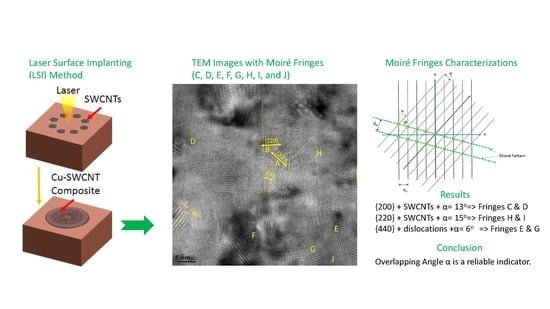
TEM Nano-Moiré Pattern Analysis of a Copper/Single Walled Carbon Nanotube Nanocomposite Synthesized by Laser Surface Implanting


1
Department of Mechanical and Aerospace Engineering, North Carolina State University, Raleigh, NC 27695-8501, USA
2
Department of Engineering Science, University West, 46129 Trollhättan, Sweden
C 2018, 4(1), 19; https://doi.org/10.3390/c4010019
Submission received: 24 January 2018
/
Revised: 6 March 2018
/
Accepted: 16 March 2018
/
Published: 20 March 2018
(This article belongs to the Special Issue Transmission Electron Microscopy and Carbon Materials)
Abstract
:In our previous studies, we have developed a wet process to synthesize a copper-single walled carbon nanotube (Cu–SWCNT) metal nanocomposite with excellent mechanical properties. The nanostructure of this Cu–SWCNT composite was confirmed independently by energy-dispersive X-ray spectroscopy mapping, spectroscopy measurements, and Transmission Electron Microscope (TEM) images with discernable SWCNT clusters in nano sizes. However, TEM images with discernable nano-sized SWCNT clusters are rare. In this paper, we present analysis of indirect TEM image patterns, such as moiré fringes, to infer the existence of SWCNT clusters within the copper matrix. Moiré fringes or patterns in the TEM images of a Cu–SWCNT nanocomposite could be generated due to the overlapping of more than one thin crystals with similar periodic arrangements of atoms, promoted by SWCNT clusters. However, the presence of moiré patterns is not a sufficient or a necessary condition for the existence of SWCNT clusters. It was found that based on the overlapping angle of two periodic arrangements, it is feasible to distinguish the moiré fringes induced by SWCNT clusters from those by other factors, such as dislocations. The ability to identify SWCNTs within the copper matrix based on indirect TEM moiré patterns helps to widen the usability of TEM images.
1. Introduction
Carbon nanotubes (CNTs), due to their exceptional structural properties, are ideal reinforcing elements to form composites for structural applications [1,2,3]. CNT-reinforced composite research first focused on polymer composites and, subsequently, metal composites. One major challenge in the synthesis of CNT–metal composites is due to the difficulty to achieve uniform dispersion of CNTs at small cluster sizes. This challenge is a result of CNTs’ tremendous surface area, up to 200 m2/g, for which van der Waals forces can lead to the formation of large clusters. Summaries and applications of metal–CNT composites can be found in several reviews, and one successful example is CNT-reinforced aluminum for high-frequency MEMS resonators [4,5,6].
Synthesis of Cu–CNT composites are considered, in general, more difficult than Al–CNT composites because copper and carbon do not form intermetallic compounds, as in the case of aluminum and carbon, which form aluminum carbide. In addition, copper and carbon are not soluble. As a result, large clusters are often formed in Cu–CNT composites to limit the strength enhancement.
1.1. Wet Synthesis of Cu–SWCNT Nanocomposite
A wet process, denoted as laser surface implanting (LSI), was reported in [7,8] for the synthesis of Cu–SWCNT nanocomposites. This process disperses SWCNTs into molten copper, followed by rapid and non-equilibrium solidification to lock SWCNTs in positions without agglomerating into large clusters. This wet process is different from the typical dry powder metallurgy method, commonly reported in the literature. Rapid and non-equilibrium solidification is achieved when the heat of the molten copper is rapidly conducted away into the copper substrate due to copper’s excellent heat conductivity. The nanostructure of the Cu–SWCNT composite is confirmed independently by energy-dispersive X-ray spectroscopy mapping, spectroscopy measurements, and TEM images with discernable SWCNT clusters, which were achieved to verify the sizes of SWCNT clusters in the nano-dimensions [9].
1.2. Difficulties in TEM Characterization of the Cu–SWCNT Nanocomposite
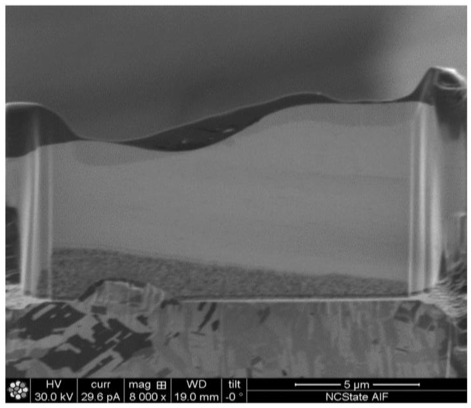
It is very rare to obtain TEM images with discernable and nano-sized clusters of SWCNT inside the copper matrix. Unless an SWCNT cluster occupies a space through the entire thickness of a TEM sample, it is unlikely an SWCNT cluster can be distinctly identified in a TEM image. This is because a TEM sample with a thickness of 40 to 50 nm contains nearly 100 to 150 layers of copper atoms, which would dominate a TEM image to obscure the carbon atoms. It is generally difficult to thin a TEM sample to be thinner than 40 nm using focus ion beam (FIB) processing. In Figure 1, a TEM sample, processed by FIB, with 40 nm thickness, is shown.
1.3. Nano-Moiré Patterns in TEM Images
Moiré patterns or fringes are produced when two similar patterns are overlapped with different spacings or orientations. In a nanostructure, moiré fringes could be due to the overlapping of two different materials with slightly different lattice spacings at the interface [10,11,12], of two differently oriented lattices of the same materials from different grains [13], of two lattices under stresses and strains [14,15], of two lattices with defects or dislocations or due to a slanted grain interface along the depth direction of the sample [16], or of two lattices with not perfectly repeatable atom arrangements under various conditions and configurations, such as those found in graphene [17,18,19,20,21]. In [22], moiré fringes are used to identify the existence of palladium clusters deposited on γ-Al2O3/NiAl{110}. Palladium clusters only produce a small contrast in TEM images, not significant enough for lattice study. However, palladium clusters could produce high contrast moiré fringes which could be exploited for information related to the lattice structure. Similarly, in this paper, we explore the use of moiré fringes to identify the existence of SWCNT clusters within the copper matrix when SWCNT clusters are not directly observed.
1.4. Hypothesis
We propose a hypothesis that within a single crystal of copper, the SWCNT clusters in the copper matrix could alter the lattice structure surrounding the clusters significantly enough to induce moiré patterns or fringes. In addition, these moiré fringes could be distinguished from other fringes induced by other conditions, such as dislocation. Note that the mere presence of moiré patterns is neither a sufficient nor a necessary condition for the existence of SWCNT within the copper matrix. The hypothesis is related to the possibility that SWCNT clusters could disrupt the atom arrangements more substantially to induce specific moiré patterns which are distinctive enough to be identified.
2. Methods
2.1. Sample Preparation and Imaging
TEM imaging was conducted on JEOL 2010F STEM at the facility of Analytical Instrumentation Facility (AIF) of North Carolina State University (NCSU), Raleigh, NC, USA. Sample preparation was carried out to thin the samples to a thickness less than 40 nm with highly smooth surface finish. TEM samples were prepared on FEI Quanta 3D Dual Beam SEM/FIB at AIF operating at 30 kV using the “Lift-Out” technique. The FIB sample preparation typically takes 3–5 h due to the thinness requirement, while TEM inspection about 7 to 10 h, and post-analysis about 6 to 9 h for one sample. Therefore, it is cost prohibitive to produce many samples to cover the entire Cu–SWCNT implant. Details of sample preparation could be found in [7,8,9].
2.2. Modeling of Moiré Fringes
Based on the hypothesis of Section 1.4, the moiré pattern of interest is related to overlapping one group of equispaced parallel lines (lattice) over another group. In Figure 2, two groups of parallel lines with different spacings and an overlapping angle, α, shown in Figure 2. For Figure 2, all clockwise angles are defined as positive.
Based on the models developed by [23] and Figure 2, the most distinct spacing of the moiré pattern can be calculated by Equation (1),
where, for the case of the Cu–SWCNT composite, is the lattice spacing of pure copper, is the altered spacing of copper, is the spacing of the moiré pattern, α is the overlapping angle of the second group with respect to the first group.
The orientation angle, ϕ, of the moiré pattern can be calculated by solving Equation (2),
If α = 0, the resulting moiré pattern is denoted as translational. Its orientation angle, ϕ, becomes zero as indicated by Equation (2), then Equation (1) can be simplified to determine its spacing as
On the other hand, if , but the lattice orientation is altered, the spacing and the orientation of the moiré pattern can be determined as
Based on Equation (5), the moiré pattern will be nearly perpendicular to the original equispaced lines if α is small. This observation is used for identifying the possible original equispaced lines.
2.3. Measurement Errors Involved in Characterizing Moiré Patterns
In the attempt to characterize moiré patterns, their spacings and orientations are measured directly from the TEM images printed on paper. The measurement errors are related to the caliper used to measure the spacing and the protractor used to measure the orientation angle. The scale bar of the TEM images used in this paper is either 2 nm or 5 nm. The repeatability in measuring a scale bar of 18 mm using a caliper is typically ±0.05 mm, confirmed by repeatedly measuring the same scale bar over ten times and verifying the range of the measured length values. In the attempt to measure the spacing of a moiré fringe, over five fringe lines will be identified, and the length across these fringes will be measured by the caliper. The measurement error is mostly associated with the uncertainty in identifying the exact location of a fringe line due to the insufficient sharpness and resolution of the TEM image. Following the same processes, the measurement error related to determining the fringe spacing is typically ±0.5 mm over at least five fringe lines. As a result, the error is ±0.1 mm per fringe. For example, in a TEM image with a 5 nm scale bar of 17.97 mm, the total span of 7 fringe lines of a moiré pattern are measured to be 19.51 mm. Converting the spacing measurement in mm to actual value in nm based on the scale bar, we determine the fringe spacing to be 0.775 nm. By considering the measurement repeatability discussed above, the uncertainty is ±0.02 nm. Therefore, the spacing is labeled as 0.78 ± 0.02 nm. For a TEM image with 2 nm scale bar, the uncertainty is ±0.01 nm. The repeatability of the angle measurement is found to be ±0.1 degree.
2.4. Diffraction Patterning and Indexing via FFT
TEM images can be converted into diffraction patterns via the fast Fourier transform (FFT) method for crystallographic analysis. The diffraction patterns in this paper were obtained using the software “Gatan Digital Micrograph” installed on JEOL 2010F to control its digital camera system, calibrated by authorized JEOL engineers. The area selected for FFT was usually about 20 nm × 20 nm. The unit of the TEM image and that of its diffraction pattern are reciprocal. The TEM image is in the real space, with a unit such as nm, while the diffraction pattern is in the reciprocal space, with a unit such as 1/nm. Some of the diffraction patterns are not provided with scale bars because these images were zoomed in to provide more details. Although technically, the patterns converted by FFT are power spectrums, not directly obtained through diffraction, these patterns contain the same characteristics as diffraction patterns, and are commonly used for diffraction indexing.
3. Results
In this section, we present experimental results, their interpretation, as well as the experimental conclusions that can be drawn.
3.1. TEM Images Showing Nano-Sized SWCNT Clusters within the Copper Matrix
Figure 3 presents an enhanced TEM image, in which distinctive SWCNT clusters embedded in the copper matrix can be discerned [9]. These SWCNT clusters, curved in shape, range from 5 to 30 nm in size. In addition, there also exist many moiré fringes in the vicinity of carbon nanotubes, pointed out by green arrows. The likely scenario for the inducement of moiré fringes could be described as follows. During the solidification of the copper, due to the presence of SWCNT clusters, a single crystal could grow until its solidification is interrupted by SWCNTs, which introduce defects to the crystal lattice. The solidification of copper then continues with a slight adjustment to the spacing or the orientation of the crystal lattice. Please refer to [9] for more TEM and diffraction images of Cu–SWCNT samples.
3.2. Diffraction Patterns and Indexing
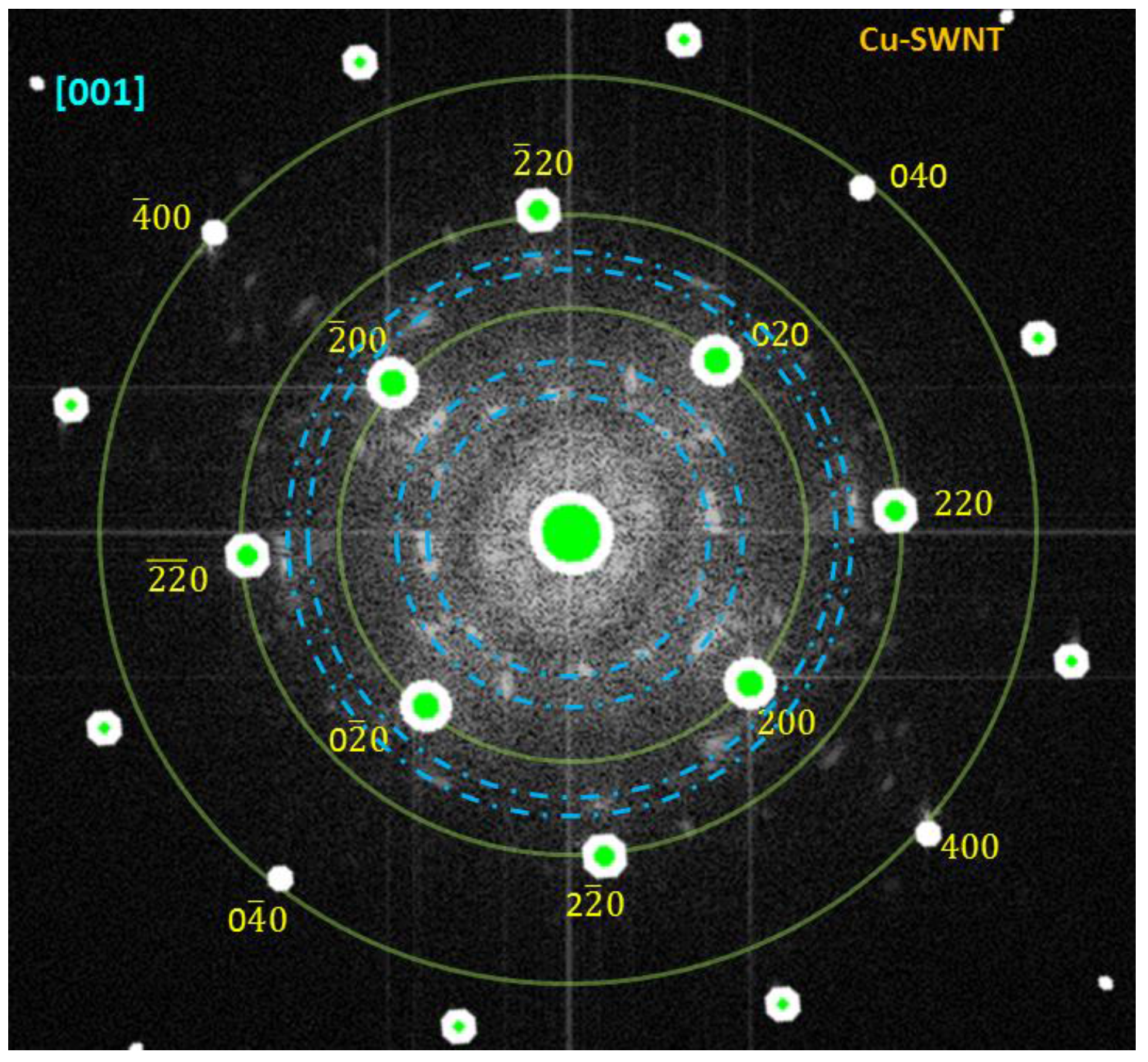
The TEM image of Figure 3 is converted to its diffraction pattern, indexed by a standard indexing template in green dots (Figure 4). The TEM image of Figure 3 is aligned with [001]. The diffraction pattern of Figure 4 contains many seemly randomly distributed clouds, due to SWCNT clusters, different from those bright dots from copper planes (not seen here due to the overlapping of a standard template). For a single piece of SWCNT, in which the carbon atoms are orderly arranged depending its chirality, its diffraction pattern could be simulated to form specific patterns [24,25]. However, for clusters of SWNTs, specific patterns could not be identified, despite that some of the brighter cloud dots appear to be located on the same distances from the center, indicated by the dot-dash rings. This ring-like spot distribution probably is the contribution due to the combination of the orderly SWCNT inner structure and the randomness of overlapping SWCNT clusters.
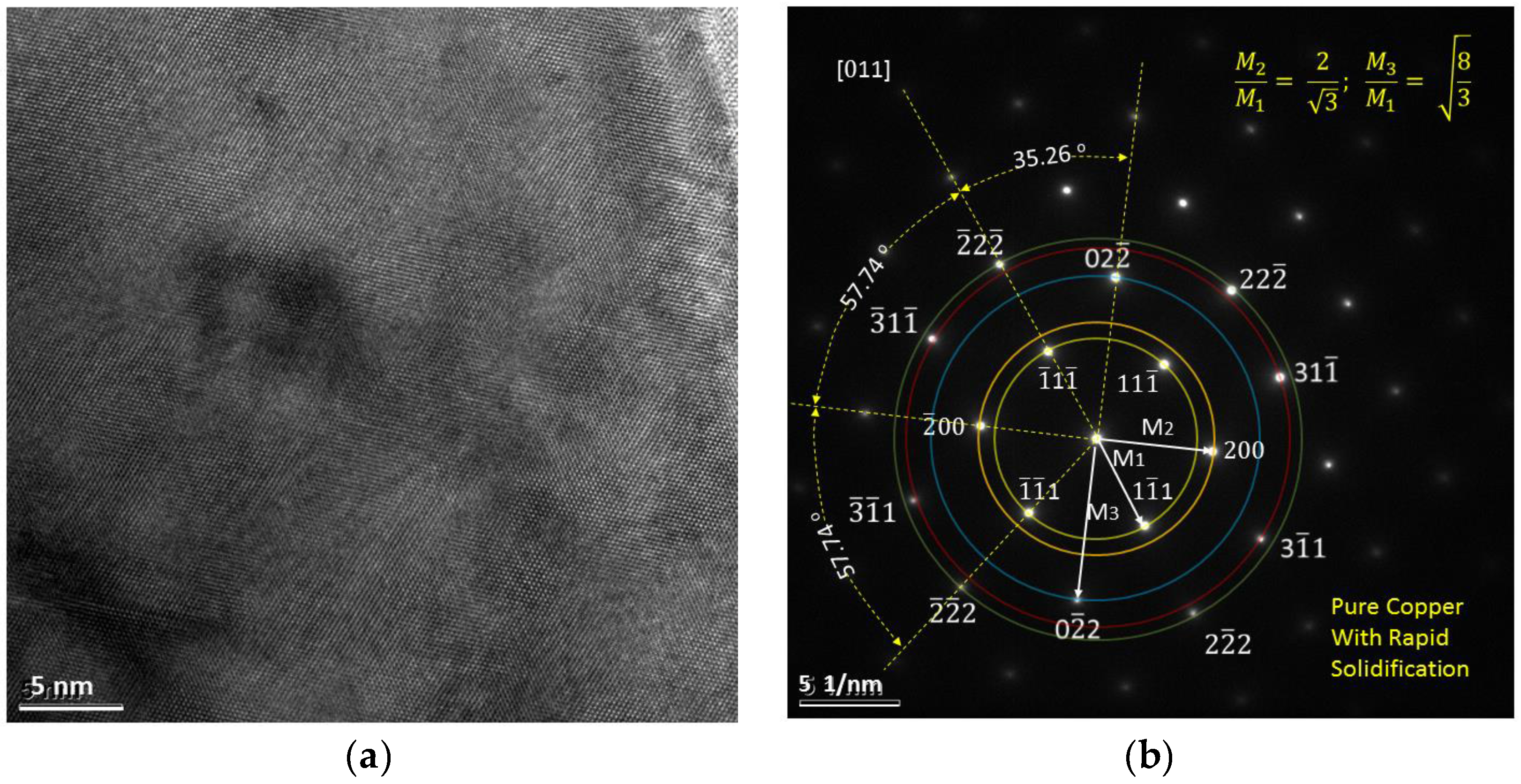
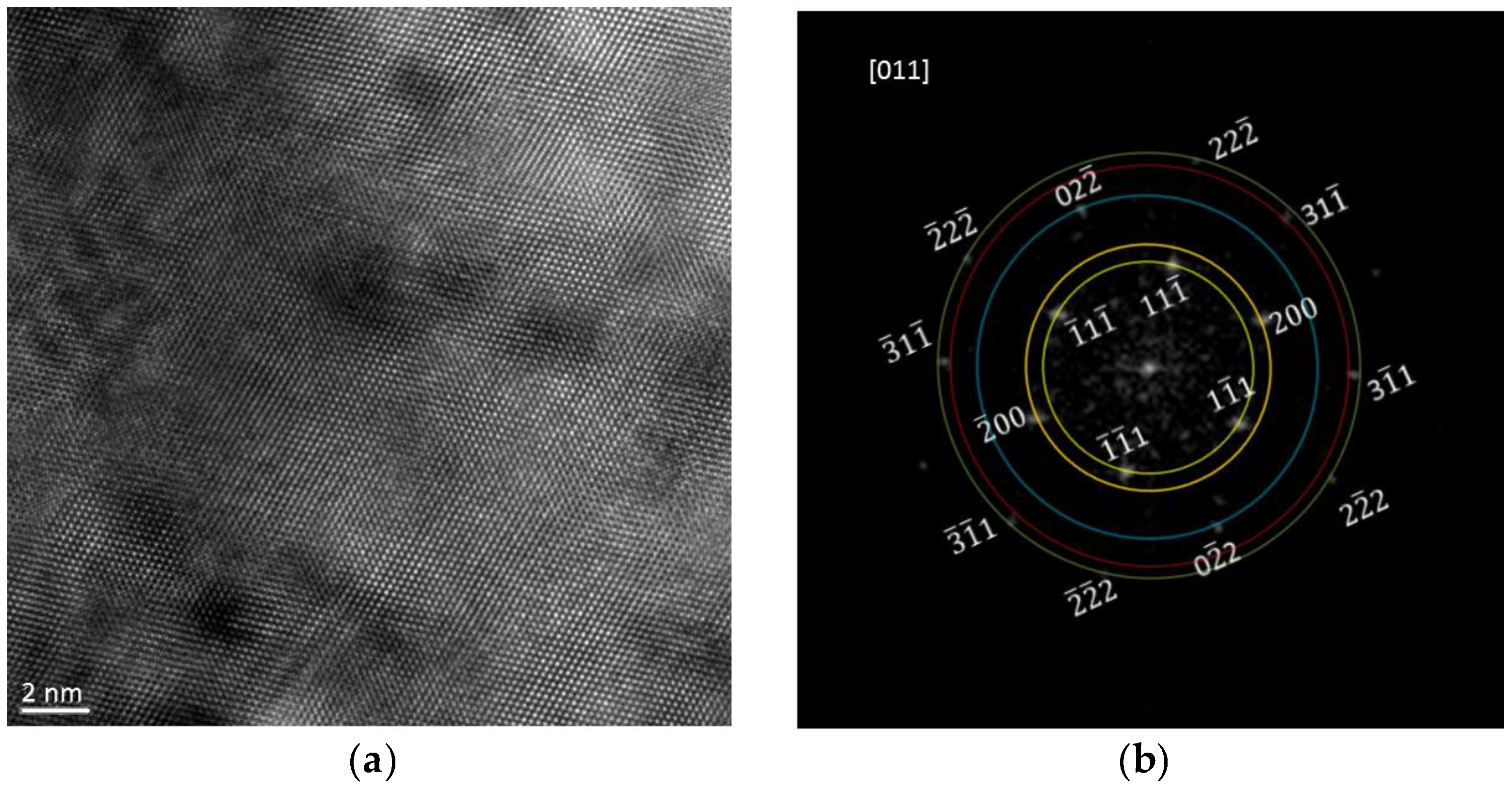
Figure 5 presents another TEM image, which likely contains one distinct SWCNT bundle in a cross-section view. In this image, the bright spots related to copper plans are clearly shown. Because the TEM image contains likely only one bundle of SWCNTs, whose carbon atoms are orderly aligned (Figure 5a), the corresponding diffraction pattern (Figure 5b) is similar to those presented in [24,25] with bright dots forming lines related to the carbon lattice planes, unlike those faint and more random clouds in Figure 4.
Based on the diffraction patterns in Figure 4 and Figure 5, it is likely that the faint clouds or bright spots outside from those of copper planes are due to SWCNTs. More evidence to support this conclusion can be found in [9]. As a result, the moiré fringes in Figure 3 and Figure 5a are likely induced by SWCNTs because of the presence of SWCNTs nearby. However, as discussed in Section 1.4, moiré fringes could be induced by other conditions. We present these cases in the next section.
3.3. Moiré Fringes not Due to SWCNTs
As shown in Figure 6, Figure 7 and Figure 8, the diffraction analysis is also applied to pure copper samples without melting and rapid solidification (annealed copper), as well as pure copper samples which were processed by the same LSI process but without introducing SWNTs (quenched copper), respectively. The enhanced diffraction patterns of Figure 6b and Figure 7b clearly indicate that no SWCNT clusters exist within the copper matrix [9]. Nonetheless, the TEM images of Figure 6a and Figure 7a still contain moiré fringes although they are not as abundant as in Figure 3.
It should be noted that for pure copper subjected to the LSI treatment, some impurities could be introduced. As a result, some cloudiness in the diffraction pattern (Figure 8b) can still be observed in a pure copper sample, although they are not as distinctive and abundant as those in Figure 4 and Figure 5b. Interestingly, even though some faint clouds are observed in Figure 8b, not many moiré fringes are observed. On the other hand, no clouds are observed in Figure 6b, but many distinctive moiré fringes exist. This confirms the statement of Section 1.4 that moiré fringes are neither a sufficient nor a necessary condition of the existence of SWCNTs. We simply could not draw much conclusion from the mere presence of moiré fringes.
In the next section, we attempt to characterize the moiré patterns based on Equations (1)–(5) with an objective to distinguish those due to SWCNT clusters from those which are not. Furthermore, the fringes identified in Figure 6a, not due to SWCNTs, will be used for comparison.
3.4. Moiré Pattern Characterization
3.4.1. Pattern #1
Figure 9 is a TEM image which contains a discernable SWCNT clusters and several fringes. Five zones, which contain equispaced lines, are identified in Figure 9, and their enlarged views are presented. In Zone A, the equispaced lines are found to be copper lattice plane family {200} because their spacing is found to be related to 0.18 nm, which is close to the 0.1807 nm, based on the published lattice constant of 0.3614 nm of copper. On the other hand, the spacings related to those of Zones B, C, D, and E are found to be 0.31, 0.62, 0.62, and 0.62 nm, respectively, with a repeatability of ±0.02 nm as discussed in Section 2.3. These spacings are basically the same or at a half value.
Because the spacing in Zone E is related to an SWCNT cluster, the fringes in Zones B, C, and D are likely direct but undefined images of SWCNT clusters. Furthermore, this SWCNT spacing is also consistent with the spacing observed in [9] and Figure 5a, where a cross-section of SWCNT cluster was observed, with four tubes over 5 nm. If the fringes in Zones B–E are indeed SWCNT clusters, it also explains why there exist many bright spots in the diffraction pattern, also shown in Figure 9. The intensities of these spots could be close to those of copper planes, due to the orderly structure of SWCNTs.
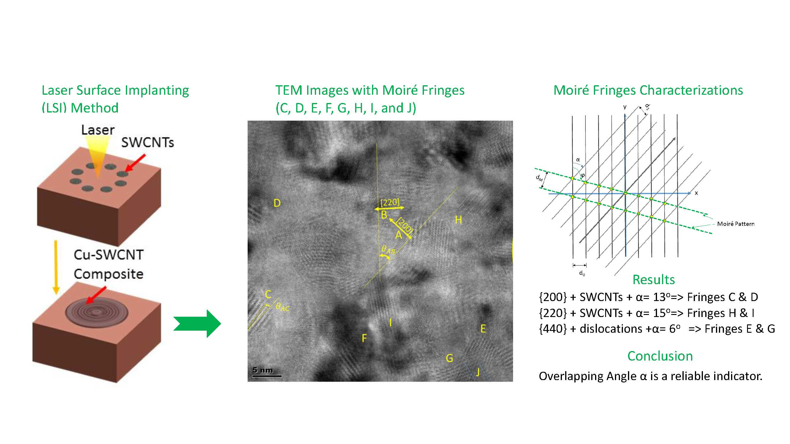
3.4.2. Pattern #2
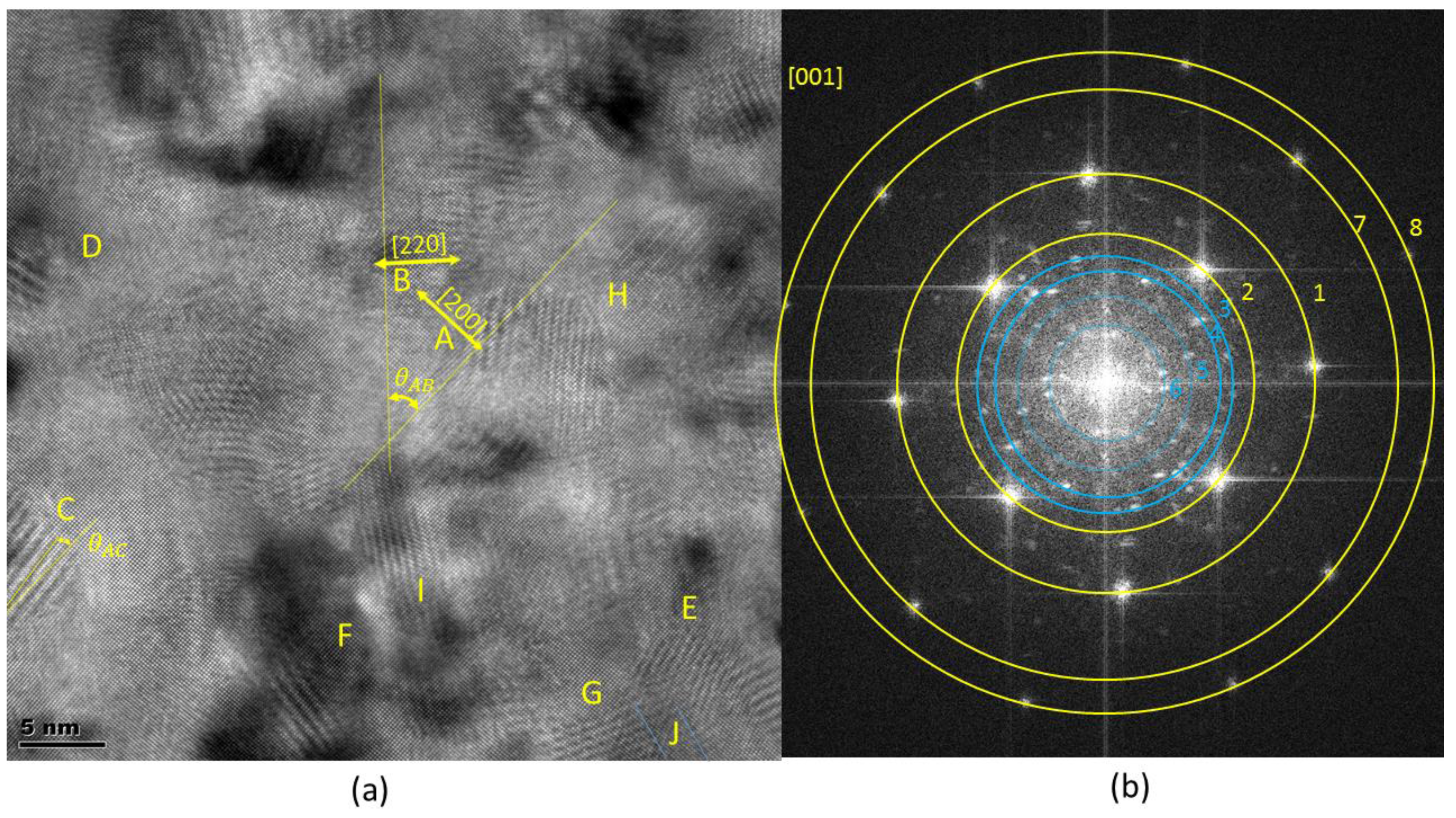
In Figure 10, another TEM image of the Cu–SWCNT composite is presented, in which many different fringes are observed. Eleven zones of patterns are identified in Figure 10, and their spacings are calculated and listed in Table 1. In the meantime, the spacings of the lattice families {220}, {200}, {400}, {420}, and {440} are listed in Table 2, along with the spacings of the rings in Figure 10b, according to its reciprocal space. Fringes in zones A and B are consistent with the spacing of the {220} and {200} lattice families, while fringes F and G in Figure 10a are likely related to Pattern #1 observed in the last section, because they are close to 0.62 nm. Fringes C, D, E, H, I, and J are apparently different. The angular orientation of these fringes with respect to Fringe A are also listed in Table 1 and defined in Figure 10a.
Fringes E and G are overlapped, and apparently form a third moiré fringe, J. The spacing of E and G are 0.55 and 0.56 nm, respectively, with a repeatability of ±0.02 nm. The angle between them is α = 51.0 ± 0.1°. We use fringes E, G, and J to test the validness of Equations (1) and (2). Based on Figure 2 and Equations (1) and (2), the moiré fringe J should have a spacing of 0.64 nm and an orientation , oriented from fringe E. The respectabilities of nm and ±0.1° are determined through programming to calculate possible results of and for the values of d0 from 0.53 to 0.57 nm, d1 from 0.54 to 0.58 nm, and from 50.9 to 51.1°. The measurements from Figure 10a are found to be 0.67 nm and 116 ± 1° with respect to fringe E. The angle measurement for fringe J is difficult because it is blurrier, and thus it suffers a greater error of ±1°. The calculated and measured values for moiré fringe of J essentially match and are within the error tolerance.
Among these fringes identified in Figure 10a, only fringe F has a spacing close to those of SWCNT clusters, as shown in Figure 9.
Fringes C and D are essentially the same spacing and are perpendicular to each other. They are closely aligned with the lattice family {200} (ring#2 in Figure 10b). Because fringe D is nearly perpendicular to the lattice plane of (200), we could assume that it is formed due to the lattice plane of (200) with a different equispaced lines at a different angle. Equations (1) and (2) can then be used to determine the pattern of the second equispaced lines. Therefore, = 0.1807 nm, based on the published value. Fringe D has an orientation , based on the definition of Figure 2 and Table 1, and its spacing is measured to be, = 0.77 nm. Solving Equations (1) and (2), we obtain nm and . Again, the ranges of these results are obtained through programming to examing possible results from possible values of dM and Because and are two unknowns of Equations (1) and (2), their values are deterministically calculated with respective to different values of d0, dM, and . The results will be meaningful only if the value of d1 matches the spacing of the {200} lattice family. Because the calculated values of are from 0.173 to 179 nm, or rounded to 0.17 to 0.18 nm, which are closely related to the published spacing of 0.1807 nm, it is highly likely that the assumption that Fringe D is induced by lattice plane (200) is true.
Similarly, for fringe C, the same calculation can be applied but for the lattice plane (020). We essentially obtain similar results, nm and .
The orientation of fringes H and I are more closely related to the lattice family of {220}. By applying the same calculation for fringe H, with = 0.1278 nm and , we obtain nm and . Similarly, for fringe I, we obtain nm and , essentially the same result as the case of fringe H. The calculated values are very consistent with their related lattice spacings, as in the cases of fringes C and D.
Fringe E is likely related to the lattice family {440}, we have = 0.0639 nm, , and the same calculation yields nm and . Similarly, for fringe G, we obtain nm and . Again, because the calculated values of are close to the spacing of {440}, , we also conclude the fringes E and G are due to the change in the orientation of the copper lattice family {440} at the locations where the fringes E and G appear.
3.4.3. Pattern #3 Found in Pure Copper Samples
We apply the same analyses of Section 3.4.2 to Figure 6a. The related spacings and orientations are listed in Table 3. The angles are measured with respect to zone A in a similar definition as the one defined in Figure 10a. Among them, lattice planes of (200), (220), and (202) are identified as fringes A, B, and C, respectively. Their spacings and orientations match the theoretical values. In addition, five additional fringes D, E, and F, are identified. D and F have essentially the same spacing at 0.91 nm, while fringe E is 0.87 nm. Note that these fringes are all at much larger spacings than those in Figure 10a. If we assume that fringes D and F are related to the lattice family {220}, we can apply the same calculation as in Section 3.4.2, and the calculated values for and are 0.1295 nm and , respectively, for fringe D and 0.1289 ± 0.0001 nm and , respectively for fringe F. The calculated value of is very close to the nominal value of 0.1278 nm.
Assuming that fringe E is related to the family {422}, we obtain nm and . The calculated values of essentially match the nominal value of 0.0738 nm.
These results are consistent with the results earlier with the calculated values matching the nominal value of the corresponding lattice values.
4. Discussion
As discussed in [9], although the SWCNT atoms within the copper matrix display diffraction patterns as seemly random bright clouds, diffusely scattered, this diffuse scattering is clearly ordered, with the {110} diffuse and {200} diffuse, indicating that the SWCNTs incorporation into the Cu-lattice is not completely random. It is likely that the SWCNTs are directionally aligned within the {200} and {220} families of planes of the fcc Cu-lattice. Beyond the ring of {220} in the diffraction pattern, there exists nearly no clouds or random bright spots. Therefore, SWCNT clusters unlikely exist within the {400}, {420}, {422}, and {440} families.
Based on the above observation, For the Cu–SWCNT samples, the fringes related to the {200} and {220} families are likely induced by SWCNT clusters, while those related to the {400}, {420}, and {440} families are not. Note the overlapping angle, of fringes related to the {200} and {220} families (C, D, H, and I) range from 13.4° to 15.0°, much higher than those related to the {440} family (E and G), which range from 6.1° to 6.4°. This angle difference most likely is due to the presence of SWCNT clusters, which could disrupt the grown of the crystalline structure during solidification more than other factors, such as dislocations.
On the other hand, for pure copper samples (Figure 6a), the overlapping angle for the fringes related to the {220} family (D and F) ranges from 7.6° to 8.0°, while the one related to the {422} family (E) of Figure 6a is 5.0°. These angles are all much lower than those induced by SWCNT clusters in Cu–SWCNT samples, while similar to those not induced by SWCNTs.
From the results above, it is concluded that the overlapping angle, could be a reliable indicator to distinguish those moiré fringes induced by SWCNT clusters from those induced by other factors.
5. Conclusions
Based on the results and discussions presented in Section 3 and Section 4, We confirm that distinct moiré patterns in the Cu–SWCNT nanocomposite could be induced due to the overlapping of more than one thin crystal with similar periodic arrangements of atoms. The patterns of the fringes induced by SWCNT clusters could be distinguished from those by other factors based on the overlapping angle of the periodic arrangements. The ability to identify SWCNTs within the copper matrix based on indirect TEM moiré patterns helps to widen the usability of TEM images.
Acknowledgments
The author would like to acknowledge N. Rajule and Y. Liu for their work in processing SWCNT–Cu samples. NSF DMII Grant #0550734 as well Engineering On Line, Department of Mechanical and Aerospace Engineering of NCSU, the CHA!N group, and the Knowledge Foundation of Sweden for their supports and assistance. The TEM work was performed in part at the Analytical Instrumentation Facility (AIF) at North Carolina State University, which is supported by the State of North Carolina and the National Science Foundation (award number ECCS-1542015). The AIF is a member of the North Carolina Research Triangle Nanotechnology Network (RTNN), a site in the National Nanotechnology Coordinated Infrastructure (NNCI).
Conflicts of Interest
The authors declare no conflict of interest. The founding sponsors had no role in the design of the study; in the collection, analyses, or interpretation of data; in the writing of the manuscript, and in the decision to publish the results.
References
- Iijima, S. Helical microtubules of graphitic carbon. Nature 1991, 354, 56–58. [Google Scholar] [CrossRef]
- Ajayan, P.M.; Zhou, O.Z. Applications of Carbon Nanotubes. In Carbon Nanotubes; Dresselhaus, M.S., Dresselhaus, G., Avouris, P., Eds.; Topics in Applied Physics; Spring: Berlin/Heidelberg, Germany, 2001; pp. 391–425. [Google Scholar]
- Endo, M.; Strano, M.S.; Ajayan, P.M. Potential Applications of Carbon Nanotubes. In Carbon Nanotubes; Jorio, A., Dresselhaus, G., Dresselhaus, M.S., Eds.; Topics in Applied Physics; Spring: Berlin/Heidelberg, Germany, 2007; pp. 13–62. [Google Scholar]
- Curtin, W.A.; Sheldon, B.W. CNT-reinforced ceramics and metals. Mater. Today 2004, 7, 44–49. [Google Scholar] [CrossRef]
- Carreño-Morelli, E. Carbon Nanotube–Metal Matrix Composites. In Dekker Encyclopedia of Nanoscience and Nanotechnology, 2ed Edition; CRC Press: Boca Raton, FL, USA, 2009; pp. 611–619. [Google Scholar]
- Agarwal, A.; Bakshi, S.R.; Lahiri, D. Carbon Nanotubes: Reinforced Metal Matrix Composites; CRC Press: Boca, FL, USA, 2011. [Google Scholar]
- Rajule, N. Laser Synthesis and Characterization of Copper-Single Walled Carbon Nanotubes Nanocomposites. Ph.D. Thesis, Department of Mechanical and Aerospace Engineering, North Carolina State University, Raleigh, NC, USA, 2014. [Google Scholar]
- Tu, J.F.; Rajule, R.; Molian, P.; Liu, Y. Laser synthesis of a copper–single-walled carbon nanotube nanocomposite via molecular-level mixing and non-equilibrium solidification. J. Phys. D Appl. Phys. 2016, 49, 495301. [Google Scholar] [CrossRef]
- Tu, J.F.; Rajule, N.; Liu, Y.; Martin, J. Nanostructure diffraction analysis of a copper/single walled carbon nanotube nanocomposite synthesized by laser surface implanting. Carbon 2017, 113, 1–9. [Google Scholar] [CrossRef]
- Hwang, C.; Geiss, R.H.; Howard, J.K. Imaging of the grain-to-grain epitaxy in NiFe/FeMn thin-film couples. J. Appl. Phys. 1988, 64, 6115–6117. [Google Scholar] [CrossRef]
- Poza, P.; Gomez-Garcia, J.; Munez, C.J. TEM analysis of the microstructure of thermal barrier coatings after isothermal oxidation. Acta Mater. 2012, 60, 7197–7206. [Google Scholar] [CrossRef]
- Zhang, X.; Meng, F.; Christianson, J.R.; Arroyo-Torres, C.; Lukowski, M.A.; Liang, D.; Schmidt, J.R.; Jin, S. Vertical heterostructures of layered metal chalcogenides by van der Waals Epitaxy. Nano Lett. 2014, 14, 3047–3054. [Google Scholar] [CrossRef] [PubMed]
- Zhang, H.; Wen, H.; Liu, Z.; Zhang, Q.; Xie, H. TEM nano-moiré evaluation for an invisible lattice structure near the grain interface. Nanoscale 2017, 9, 15923–15933. [Google Scholar] [CrossRef] [PubMed]
- Xie, H.; Liu, Z.; Fang, D.; Dai, F.; Gao, H.; Zhao, Y. A study on the digital nano-moiré method and its phase shifting techniques. Meas. Sci. Technol. 2004, 15, 1716–1721. [Google Scholar] [CrossRef]
- Link, T.; Epishin, A.; Brückner, U.; Portella, P. Increase of misfit during creep of superalloys and its correction with deformation. Acta Mater. 2000, 48, 1981–1994. [Google Scholar] [CrossRef]
- Ohnogi, H.; Isshiki, T.; Sasaki, S.; Sajurai, S. Intriguing transmission electron microscopy images observed for perpendicularly oriented cylindrical microdomains of block copolymers. Nanoscale 2014, 6, 10817–10823. [Google Scholar] [CrossRef] [PubMed]
- Luican, A.; Li, G.; Reina, A.; Kong, J.; Nair, R.R.; Novoselov, K.S.; Geim, A.K.; Andrei, E.Y. Single-layer behavior and its breakdown in Twisted graphene layers. Phys. Rev. Lett. 2011, 106, 12682. [Google Scholar] [CrossRef] [PubMed]
- Macdonald, A.H.; Bistritzer, R. Graphene moiré mystery solved? Nature 2011, 474, 453–454. [Google Scholar] [CrossRef] [PubMed]
- Brown, L.; Hovden, R.; Huang, P.; Wojcik, M.; Muller, D.A.; Park, J. Twinning and twisting of tri- and bilayer graphene. Nano Lett. 2012, 12, 1609–1615. [Google Scholar] [CrossRef] [PubMed]
- Robertson, A.W.; Warner, J.H. Atomic resolution imaging of graphene by transmission electron microscopy. Nanoscale 2013, 5, 4079–4093. [Google Scholar] [CrossRef] [PubMed]
- Kim, J.H.; Kim, K.; Lee, Z. The hide-and-seek of grain boundaries from moiré pattern fringe of two-dimensional graphene. Sci. Rep. 2015, 5, 12508. [Google Scholar] [CrossRef] [PubMed]
- Nepijko, S.; Klimenkov, M.; Adelt, M.; Kuhlenbeck, H.M.; Schlogl, R.; Freund, H.-J. Structural investigation of palladium clusters on γ-Al2O3/NiAl(110) with transmission electron microscopy. Langmuir 1999, 15, 5309–5313. [Google Scholar] [CrossRef]
- Oster, G.; Wasserman, M.; Zwerling, C. Theoretical interpretation of moiré patterns. J. Opt. Soc. Am. 1964, 54, 169–175. [Google Scholar] [CrossRef]
- Colomer, J.-F.; Henrard, L.; Lambin, P.H.; Van Tendeloo, G. Electron diffraction and microscopy of single-wall carbon nanotube bundles produced by different methods. Eur. Phys. J. B 2002, 27, 111–118. [Google Scholar] [CrossRef]
- Qin, L.-C. Electron Diffraction from Carbon Nanotubes. Rep. Prog. Phys. 2006, 69, 2761–2821. [Google Scholar] [CrossRef]
Figure 1.
A TEM sample of 40 nm thickness processed by focus ion beam (FIB).

Figure 2.
Two equispaced parallel lines and their resulting moiré fringes.
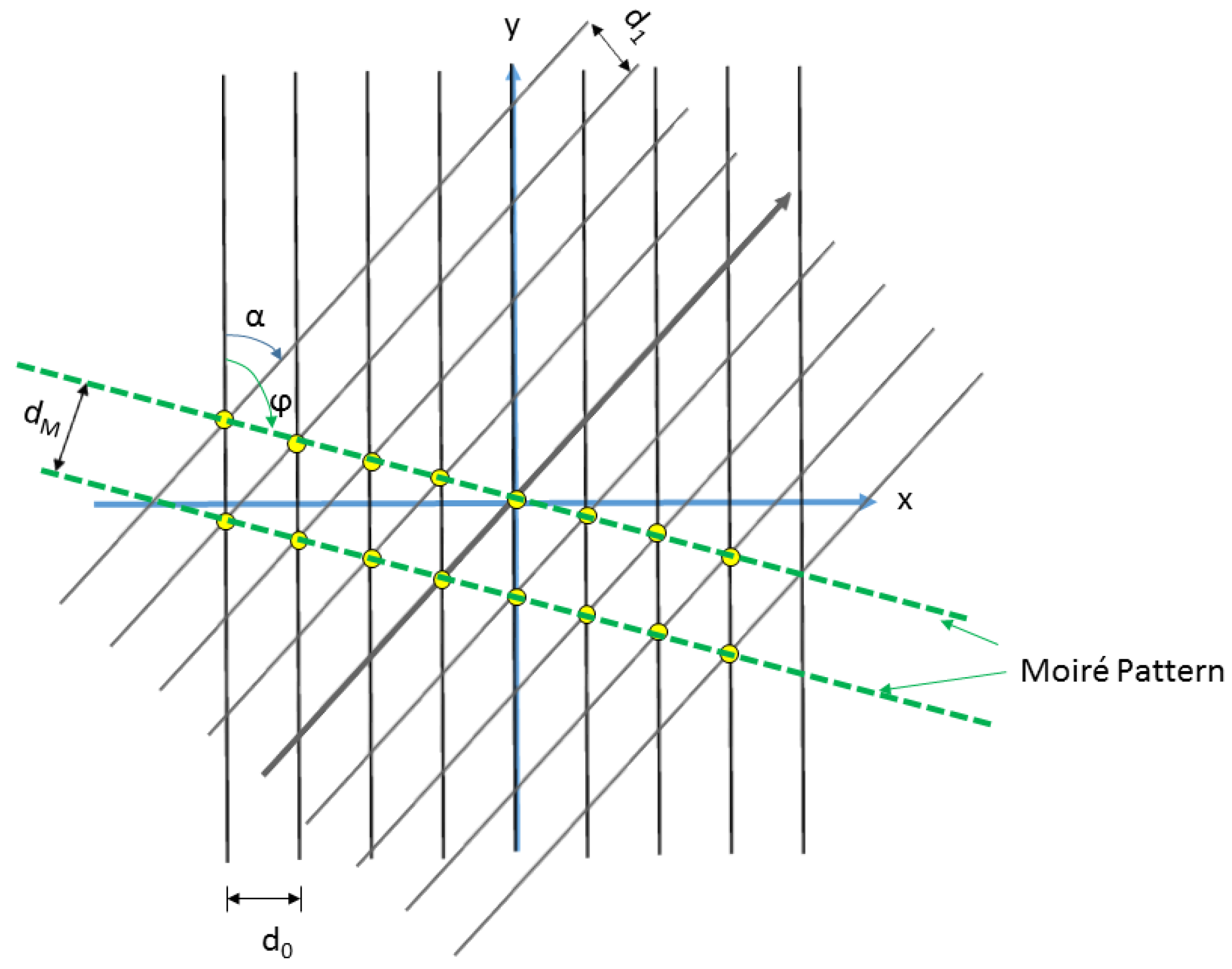
Figure 3.
A TEM image with discernable single walled carbon nanotube (SWCNT) clusters within copper matrix; an enhanced image from [9].
Figure 3.
A TEM image with discernable single walled carbon nanotube (SWCNT) clusters within copper matrix; an enhanced image from [9].
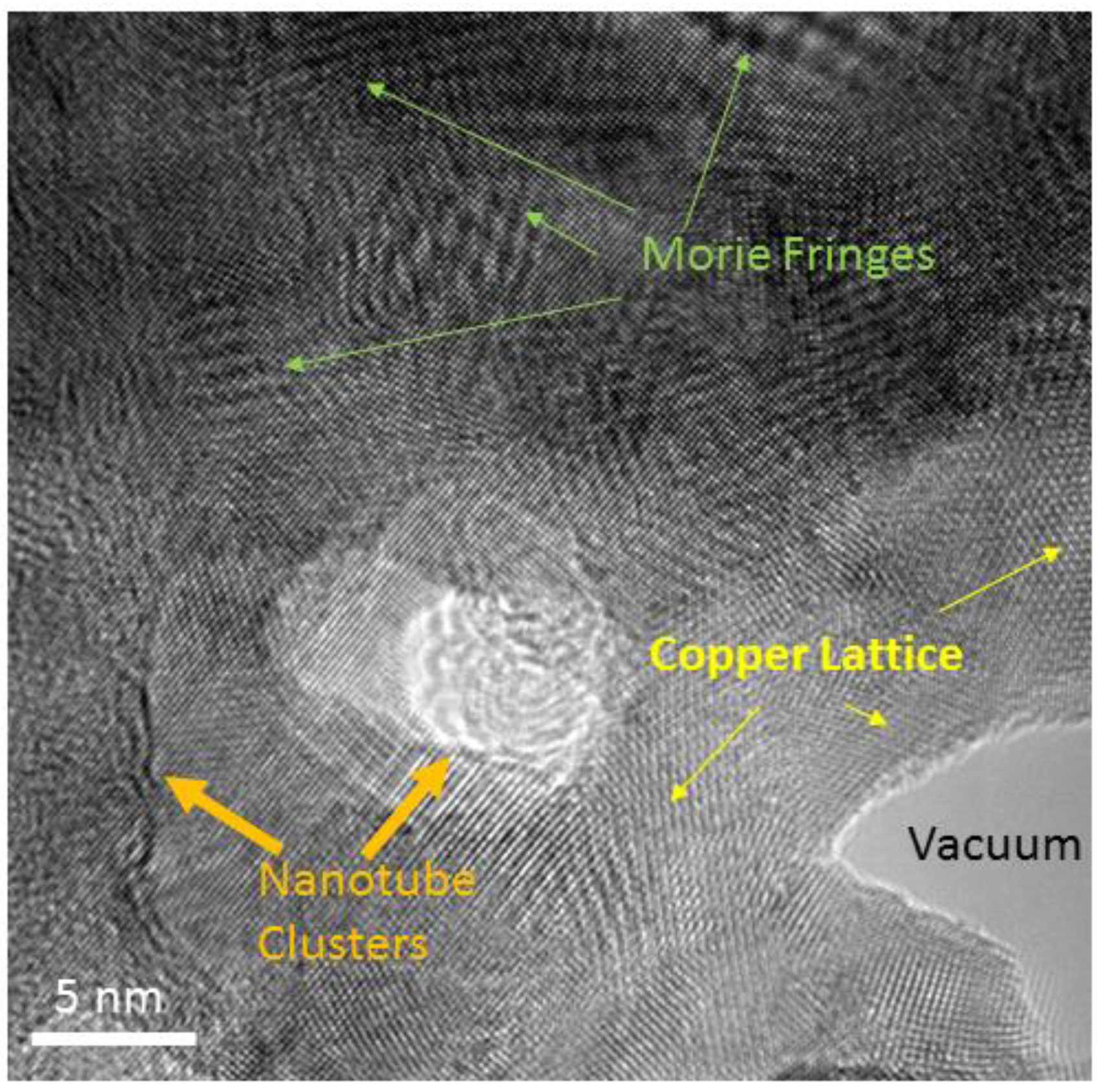
Figure 4.
Overlapped diffraction pattern of Cu–SWNT and a standard template.

Figure 5.
The TEM image of Cu–SWCNT with pattern #1 fringes. (a) the TEM image; (b) corresponding diffraction pattern via FFT.
Figure 5.
The TEM image of Cu–SWCNT with pattern #1 fringes. (a) the TEM image; (b) corresponding diffraction pattern via FFT.
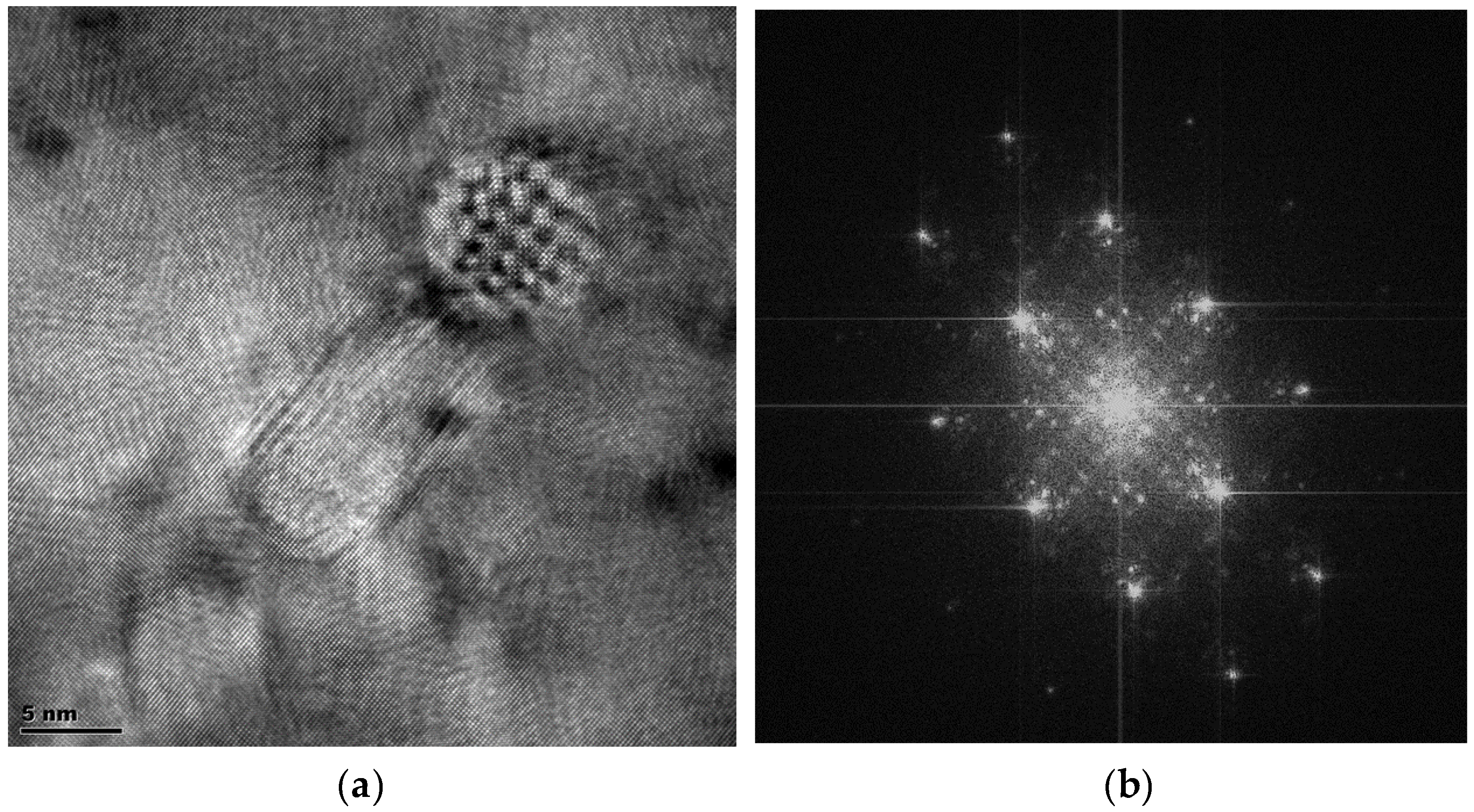
Figure 6.
TEM image and its indexed diffraction pattern of an annealed copper sample, which is an enhanced image from [9]. (a) the TEM image with moiré patterns identified by letters; (b) corresponding indexed diffraction pattern via FFT.
Figure 6.
TEM image and its indexed diffraction pattern of an annealed copper sample, which is an enhanced image from [9]. (a) the TEM image with moiré patterns identified by letters; (b) corresponding indexed diffraction pattern via FFT.
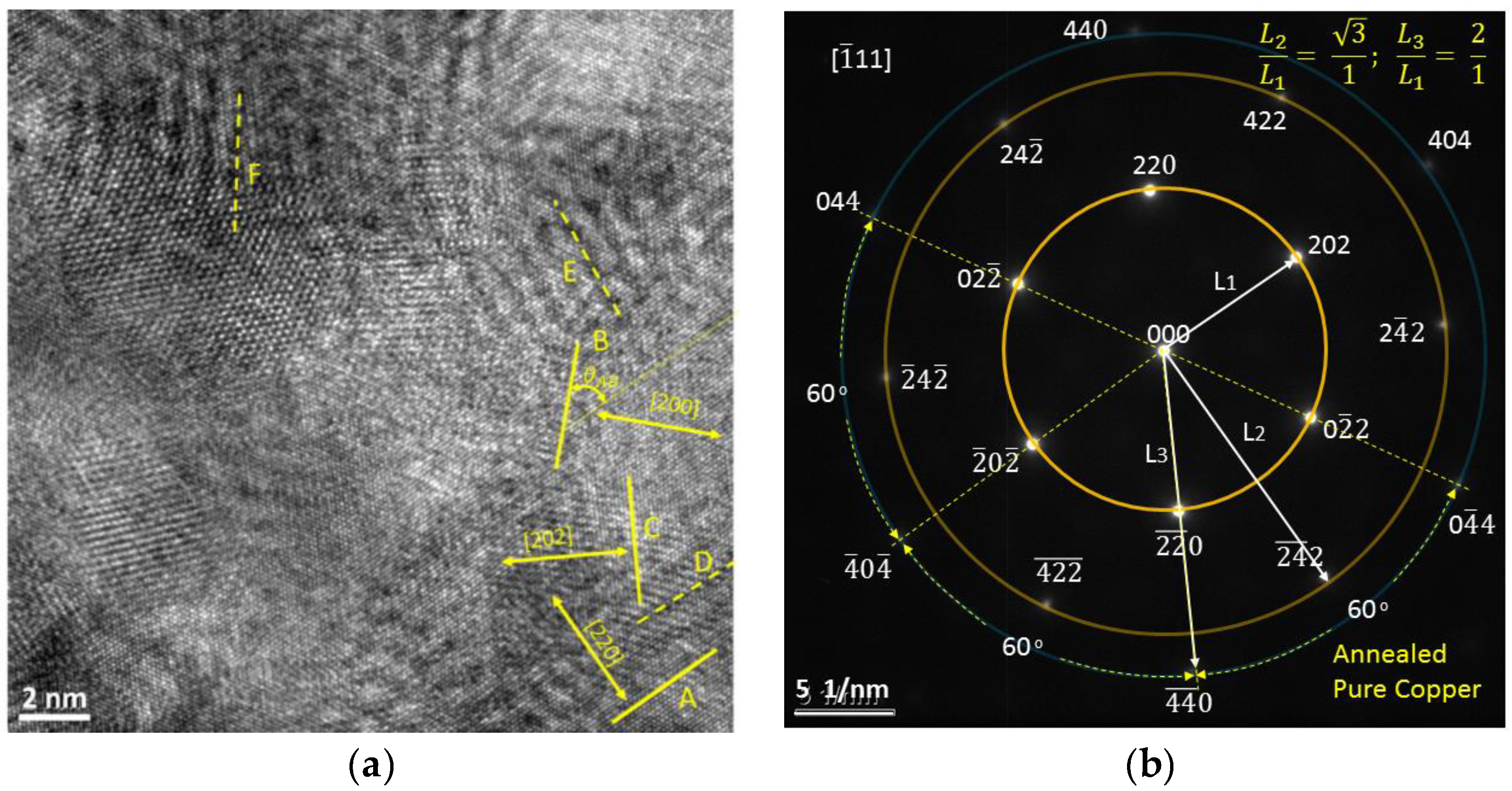
Figure 7.
TEM image and its indexed diffraction pattern of a pure copper sample subjected to the LSI treatment without SWCNT, which is an enhanced image from [9]. (a) the TEM image; (b) corresponding indexed diffraction pattern via FFT.
Figure 7.
TEM image and its indexed diffraction pattern of a pure copper sample subjected to the LSI treatment without SWCNT, which is an enhanced image from [9]. (a) the TEM image; (b) corresponding indexed diffraction pattern via FFT.

Figure 8.
TEM image and its indexed diffraction pattern of a pure copper sample subjected to the LSI treatment without SWCNT. (a) the TEM image; (b) corresponding indexed diffraction pattern via FFT
Figure 8.
TEM image and its indexed diffraction pattern of a pure copper sample subjected to the LSI treatment without SWCNT. (a) the TEM image; (b) corresponding indexed diffraction pattern via FFT

Figure 9.
The TEM image of Cu–SWCNT, its diffraction pattern, and spacings.
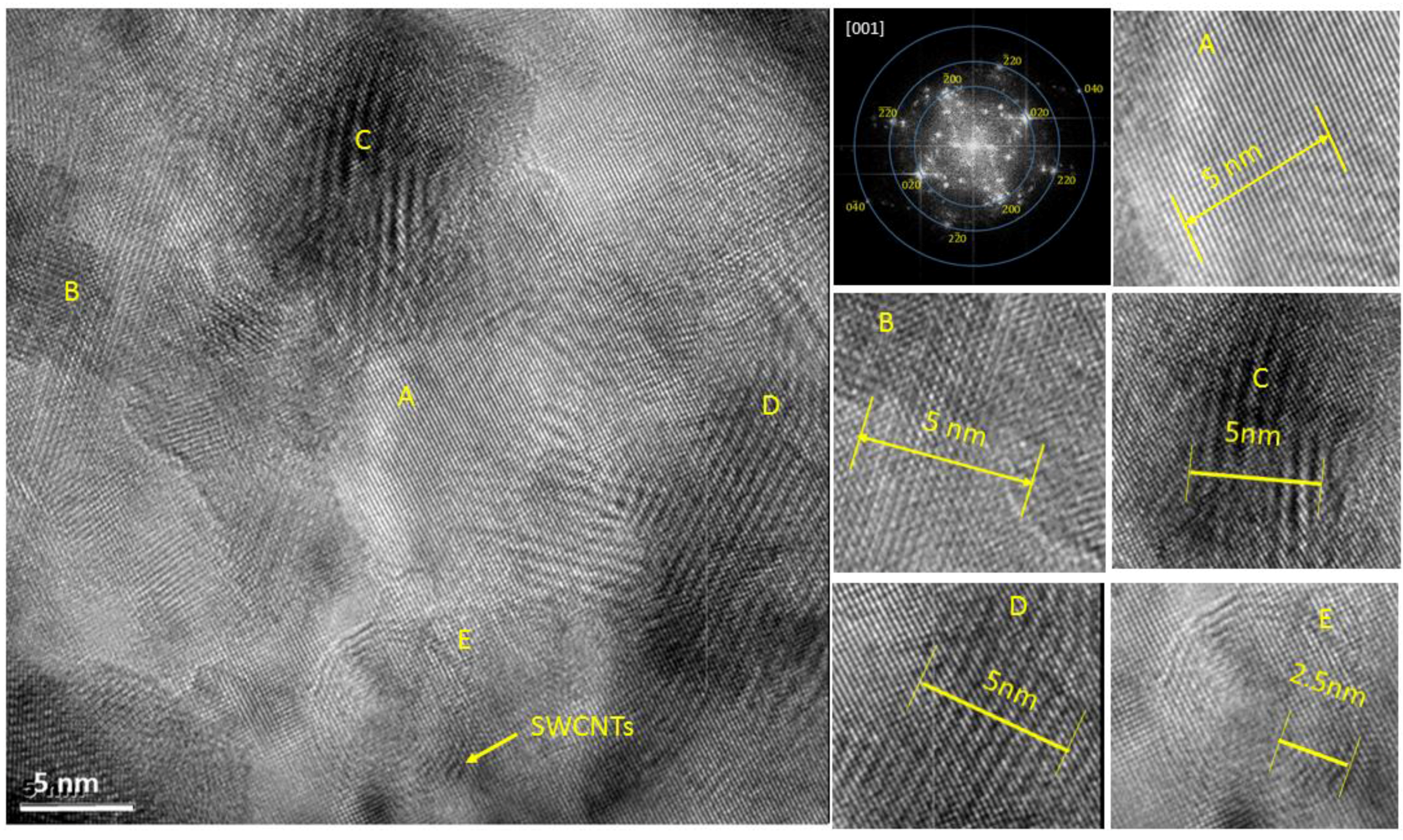
Figure 10.
The TEM image of Cu–SWCNT, its diffraction pattern, and spacings.


Table 1.
Spacings of fringes of Figure 10a.
Table 1.
Spacings of fringes of Figure 10a.
| Fringes Zone | A | B | C | D | E | F | G | H | I | J |
|---|---|---|---|---|---|---|---|---|---|---|
| Spacing, nm | 0.18 | 0.13 | 0.78 | 0.77 | 0.55 | 0.64 | 0.56 | 0.49 | 0.49 | 0.67 |
| ±0.02 nm | ||||||||||
| Angle | 0 | 45.0 | 4.3 | 94.2 | 21.6 | 78.9 | −29.4 | 37.6 | 51.2 | 86 * |
| ±0.1 degree |
* the angular error is ±1° for fringe J.
Table 2.
Reciprocal spacings of rings on Figure 10b.
Table 2.
Reciprocal spacings of rings on Figure 10b.
| Ring # | 1 | 2 | 3 | 4 | 5 | 6 | 7 | 8 | |
|---|---|---|---|---|---|---|---|---|---|
| Lattice Family | {220} | {200} | - | - | - | - | {400} | {420} | {440} |
| Spacing (nm) | 0.1278 | 0.1807 | 0.21 | 0.24 | 0.31 | 0.47 | 0.090 | 0.081 | 0.064 |
Table 3.
Spacings of fringes of Figure 6a.
Table 3.
Spacings of fringes of Figure 6a.
| Fringes Zone | A | B | C | D | E | F |
|---|---|---|---|---|---|---|
| Spacing, nm | 0.13 | 0.18 | 0.13 | 0.91 | 0.87 | 0.91 |
| ±0.01 nm | ||||||
| Angle | 0 | 45.0 | 60.0 | −0.8 | 80.7 | 49.5 |
| ±0.1 degree |
© 2018 by the author. Licensee MDPI, Basel, Switzerland. This article is an open access article distributed under the terms and conditions of the Creative Commons Attribution (CC BY) license (http://creativecommons.org/licenses/by/4.0/).
Share and Cite
MDPI and ACS Style
Tu, J.F. TEM Nano-Moiré Pattern Analysis of a Copper/Single Walled Carbon Nanotube Nanocomposite Synthesized by Laser Surface Implanting. C 2018, 4, 19. https://doi.org/10.3390/c4010019
AMA Style
Tu JF. TEM Nano-Moiré Pattern Analysis of a Copper/Single Walled Carbon Nanotube Nanocomposite Synthesized by Laser Surface Implanting. C. 2018; 4(1):19. https://doi.org/10.3390/c4010019
Chicago/Turabian StyleTu, Jay F. 2018. "TEM Nano-Moiré Pattern Analysis of a Copper/Single Walled Carbon Nanotube Nanocomposite Synthesized by Laser Surface Implanting" C 4, no. 1: 19. https://doi.org/10.3390/c4010019
Note that from the first issue of 2016, this journal uses article numbers instead of page numbers. See further details here.