Transmission Electron Microscopy of Carbon: A Brief History


Electron Microscopy Laboratory, Department of Chemistry, University of Reading, Whiteknights, Reading RG6 6AF, UK
C 2018, 4(1), 4; https://doi.org/10.3390/c4010004
Submission received: 21 December 2017
/
Revised: 5 January 2018
/
Accepted: 8 January 2018
/
Published: 12 January 2018
(This article belongs to the Special Issue Transmission Electron Microscopy and Carbon Materials)
Abstract
:Transmission electron microscopy (TEM) has been used in the study of solid carbon since the 1940s. A number of important forms of carbon have been discovered through the use of TEM, and our understanding of the microstructure of carbon has largely been gained through the application of TEM and associated techniques. This article is an attempt to present an historical review of the application of TEM to carbon, from the earliest work to the present day. The review encompasses both graphitic carbon and diamond, and spectroscopic techniques are covered, as well as imaging. In the final section of the review, the impact of aberration-corrected TEM on current carbon research is highlighted.
1. Introduction
Solid carbon exists in a huge variety of different forms, including graphite, diamond, graphene, nanotubes, glassy carbon, coke, and char. Much of what we know about the microstructure of these materials has come from the application of transmission electron microscopy. While X-ray diffraction can provide more accurate crystallographic information, and spectroscopic techniques can be used to determine the overall order of the carbon and the sp2/sp3 ratio, transmission electron microscopy (TEM) has an unrivalled ability to reveal the microscopic structure, potentially down to the atomic level. This article aims to trace the history of TEM studies of carbon, from the earliest work in the 1940s to current research using aberration-corrected microscopes. An attempt is made to identify landmarks in the field in 20 year periods beginning in 1940. To begin, a brief outline of the history of transmission electron microscopy is given.
2. The Development of Transmission Electron Microscopy
Max Knoll and Ernst Ruska of the Berlin Technische Hochschule demonstrated the first transmission electron microscope in 1931 [1], and in 1933 achieved a resolution greater than that of light with this microscope. Working at Siemens, Ruska helped to develop the first commercial TEM in 1939. At the same time, Otto Scherzer in Darmstadt was laying the basis for the theory of electron optics [2]. After the war, a number of companies developed commercial TEMs, notably JEOL in Japan and Philips in Europe, and the technique grew in importance in both biology and materials science. Biological applications of TEM are outside the scope of this review, but a few milestones in TEM of materials will be mentioned. In 1949 Robert Heidenreich of Bell Labs pioneered the study of metals by TEM, using an electrolytic method to prepare sufficiently thin specimens [3]. Seminal work on defects in metals was subsequently carried out by Peter Hirsch and colleagues in Cambridge who reported the first observations of moving dislocations in aluminium [4] and by Walter Bollman of the Battelle Laboratory in Geneva, who observed dislocations in stainless steel [5].
In 1956 James Menter, working at the Tube Investments research labs near Cambridge, obtained the first direct lattice images of crystals [6]. The specimens he imaged were thin crystals of copper and platinum phthalocyanine, both of which have relatively large lattice spacings, of the order of 1.2 nm. Tsutomu Komoda and colleagues from the Hitachi Labs in Tokyo reported similar images in 1958 [7]. In 1965, Komoda recorded lattice images with a spacing of 0.235 nm from thin films of gold [8], while the first lattice images of graphite were obtained by Heidenreich and colleagues in 1968 [9], as discussed below. It is important to recognise, however, that most of these early lattice images were not directly interpretable in terms of the real crystal structure. True “structure imaging” had to await the development, in the 1970s and 1980s, of improved electron lenses and of accompanying computer techniques for image simulation.
An experimental scanning transmission electron microscope (STEM) had been built by Manfred von Ardenne in Berlin before the war [10]. However, it was the work of Albert Crewe at the University of Chicago in the late 1960s that led to the development of STEM as a practical technique. Crewe employed a field emission gun to give the coherent and intense source of electrons needed for STEM. He also developed an annular dark field detector, and using this detector was able to image individual heavy atoms [11]. Commercial STEMs became available in the 1970s. These early instruments were generally dedicated high vacuum microscopes. Today it is more usual for a scanning unit to be incorporated into a conventional TEM.
Another technique associated with TEM should be mentioned. Electron energy loss spectroscopy (EELS) involves analysing the energy distribution of electrons that have passed through a TEM specimen [12]. It is particularly useful for light element analysis, and can provide information about bonding and oxidation state. Since the early 1990s, EELS has been increasingly used to study both sp2 and sp3 carbon and has helped to provide answers to some long-standing issues in carbon science.
By the mid-1990s, progress in improving the resolution of conventional and scanning transmission electron microscopes had all but drawn to a halt, and it was clear that some major innovations would be needed if further improvements were to be made. Scherzer had realised in the 1930s that the resolution of electron lenses was ultimately limited by spherical and chromatic aberration. Although attempts had been made over the years to design correctors that would compensate for these aberrations, none were completely successful. The development of fully effective aberration correctors in the late 1990s by scientists including Harald Rose (a student of Scherzer), Maximilian Haider, and Knut Urban was therefore a hugely significant advance [13]. Distances smaller than 0.1 nm could now be resolved by both TEM and STEM. As discussed in Section 3.4 below, few areas have benefitted more from this new generation of microscopes than carbon science. More detailed historical reviews of TEM, particularly as applied to materials science, and of aberration-corrected TEM, can be found in references [14,15,16,17]. A previous review of TEM of carbon, focusing mainly on relatively recent work, has also been given [18].
3. Landmarks in the Application of TEM to Carbon
3.1. 1940s and 1950s
It appears that carbon black was one of the first carbon materials to be studied in the TEM [19,20,21]. These early studies established that carbon black consisted of aggregated spheroidal particles, with the individual particles being typically 50–100 nm in size. Work by Hofmann and Höper [19] showed that the particles became faceted on heating to 3000 °C. At this time the resolution of the best TEMs was around 10 nm, so there was no possibility of resolving the individual graphitic planes.
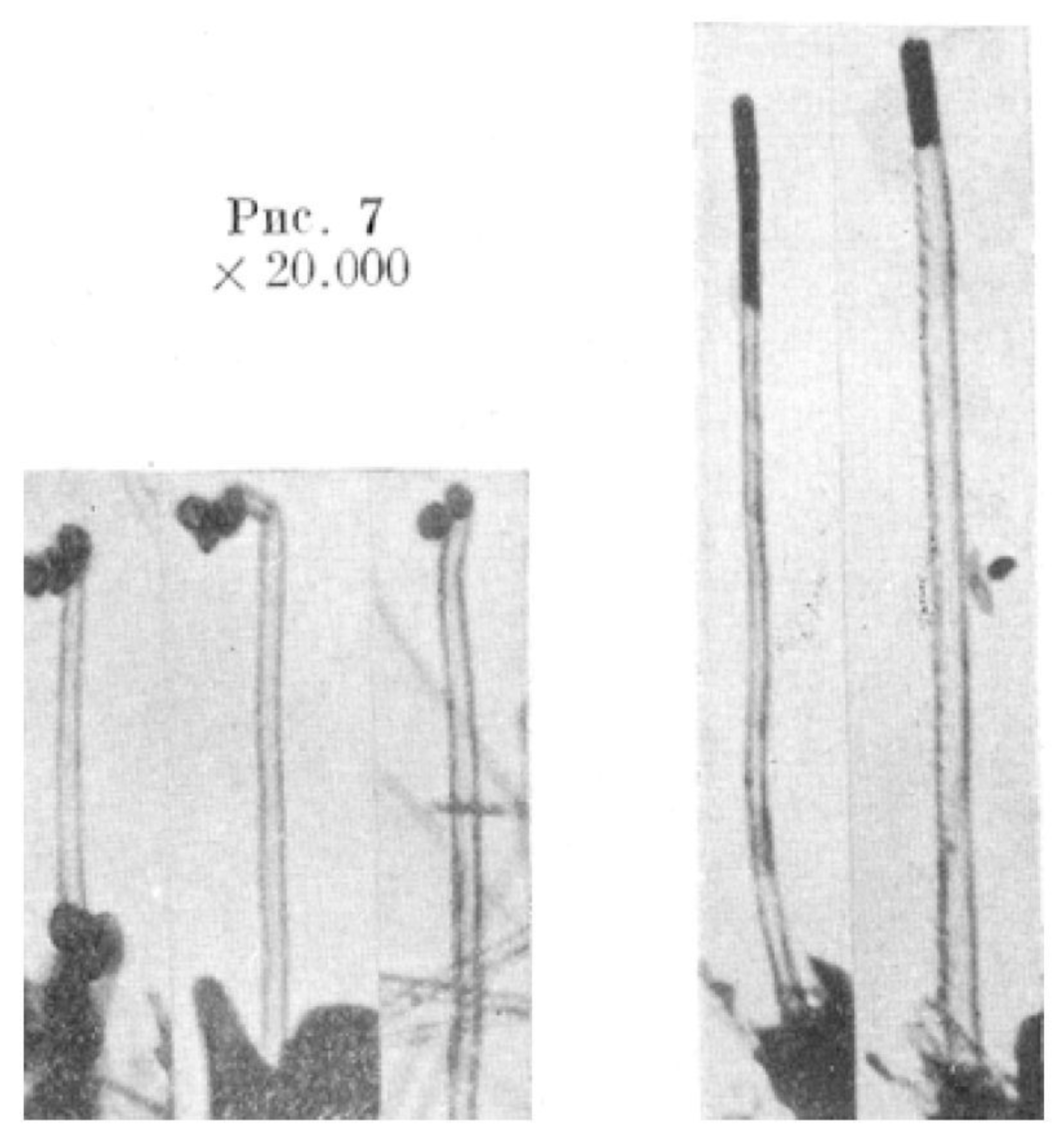
Perhaps the most notable early paper on TEM of carbon was a 1952 study of catalytically grown carbon filaments by the Russian scientists Radushkevich and Lukyanovich [22]. As can be seen in Figure 1, their images clearly showed that the filaments were tubular. This is now recognised as the first observation of the structures now known as carbon nanotubes. However, at the time the article was hardly noticed by Western scientists. Due to the cold war, access to Russian scientific publications was limited, and papers in Russian did not generally appear in literature databases. Only very recently has the achievement of these scientists been fully recognised [23].
In 1953, British scientists also published TEM images of carbon “vermicules”, some of which appeared to be helical, in a Nature paper entitled “An unusual form of carbon” [24]. These structures, which are almost certainly nanotubes, were discovered in studies of carbon deposited on the brickwork of blast furnaces. They were apparently formed from the catalytic decomposition of carbon monoxide by iron oxide particles in the bricks. The paper had no references, and it is very unlikely that the authors were aware of the earlier Russian work.
3.2. 1960s and 1970s
In 1960, Roger Bacon of the Union Carbide Corporation was carrying out experiments on the triple point of carbon using a direct current (DC) carbon arc furnace when he noticed fine filaments growing from the vapour phase on the negative electrode. Examination of the fibres in the TEM showed that they had a scroll-like structure, with diameters ranging from a fraction of a μm to over 5 μm [25]. Bacon christened the fibres “graphite whiskers”, and showed that they had exceptional mechanical properties, close to the ideal value for a graphite cylinder. Although the whiskers never became a commercial product, owing to their high production cost, for many years they were the strongest and stiffest carbon fibres available, and in some ways represented a precursor to fullerene-related carbon nanotubes.
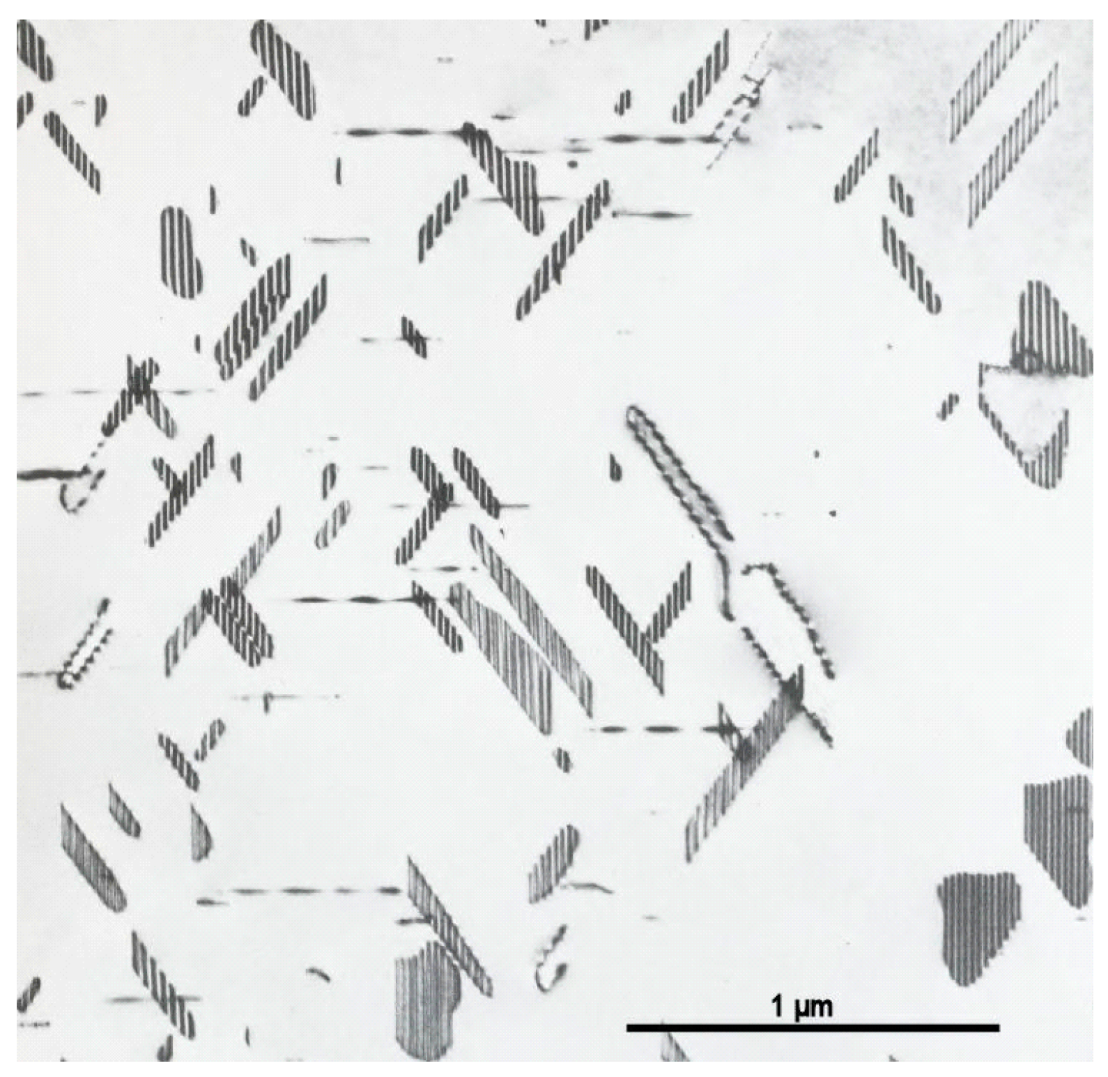
One of the most important applications of graphite over the past 60 years has been as a neutron moderator in nuclear reactors. The very first nuclear reactor, the Chicago “squash court” reactor, used graphite as a neutron moderator, and many commercial reactors, both gas-cooled and water-cooled, have used graphite in this way. Understanding the structure and properties of graphite therefore became a priority for the nuclear industry, particularly in view of the fact that that radiation effects on the structure of graphite may have played a role in the Windscale reactor fire of 1957. As a result, much important and fundamental work on the structure of graphite was carried out using conventional bright and dark field TEM during the 1960s (e.g., [26,27,28]), as discussed in reviews by Amelinckx [29] and Thrower [30]. Important studies of graphite reactivity, which also originated in nuclear-related research, were also carried out by John Meurig Thomas and colleagues, firstly using optical microscopy [31] and later using TEM [32].
Another area of carbon science that benefitted from nuclear-related research is the study of catalytically-grown carbon tubes. As noted above, these were first observed in 1952 by Russian scientists, but little further work was done in this area until the studies of R.T.K. ”Terry” Baker and colleagues at the UK’s Atomic Energy Research Establishment, from about 1970. Baker was investigating the formation of carbon deposits on nuclear fuel-pins in gas-cooled reactors, and in order to model these processes he employed controlled atmosphere transmission electron microscopy [33]. In this technique, which had been pioneered by Marton as early as 1935 [34], a differential pumping system allows the specimen to be exposed to relatively high gas pressures while being heated. Baker used this method to directly observe the growth of filamentous carbon by the catalytic decomposition of hydrocarbons on metal particles, gaining important insights into the growth mechanism. Although Baker’s work was aimed at preventing carbon filament formation, other workers, notably Morinobu Endo [35], suggested that the filaments could be valuable materials in their own right. The discovery of fullerene-related nanotubes by Iijima in 1991 (see below) stimulated a renewed burst of fundamental work on the growth and structure of catalytically-grown carbon filaments, and much of this work drew on Baker’s pioneering studies.
A major breakthrough in TEM of carbon came in 1968 when the first lattice images of graphitic carbon were obtained by Robert Heidenreich of Bell Labs and colleagues [9]. Images of graphitized carbon black were reported in which the approximately 0.34 nm spacing was clearly visible. A typical image of graphitized carbon black, taken a few years later by Ban [36], is shown in Figure 2. The ability to resolve graphitic structure directly prompted a rapid expansion of TEM work on sp2-based carbon materials, including carbon fibres [37], glassy carbon [38] microporous carbon [39], and coal [40]. Several reviews of these early studies have been given [36,41,42].
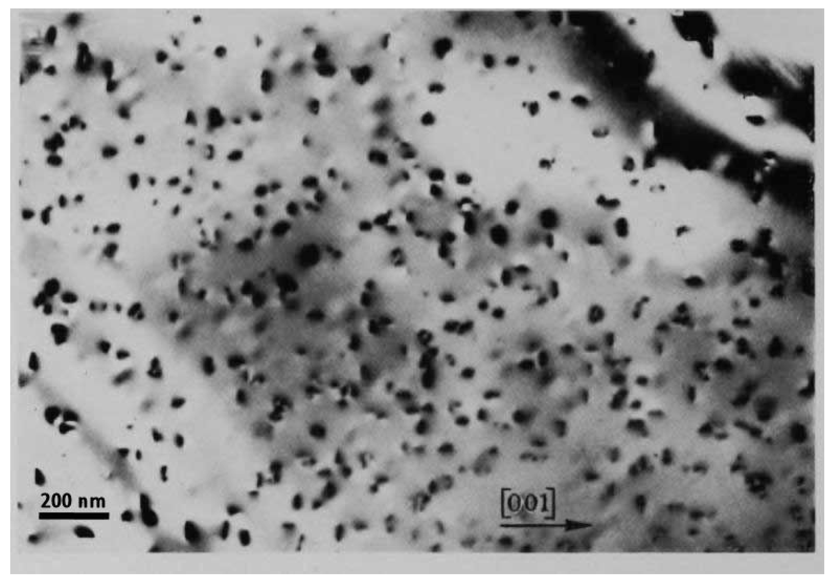
The study of diamond by transmission electron microscopy was pioneered in 1962 by Trevor Evans and Cornelius Phaal of Reading University [43]. These workers showed that natural diamonds could be thinned by oxidation to the point where imaging in the TEM became possible. In this way, they achieved the first images of platelets on the {100} lattice planes in type Ia diamonds, an example of which is shown in Figure 3. Such defects were absent in type II diamonds, but both types contained dislocations (diamonds are classified into different types depending on the kind of impurities they contain). The precise nature of the platelets, which had been first postulated by F.C. Frank in 1956 to explain anomalous features in X-ray diffraction patterns of type Ia diamond [44], was a subject of controversy for many years. Evans and Phaal initially suggested that the platelets contained nitrogen, which is the main impurity in type Ia diamonds. A detailed structural model of nitrogen-containing platelets was proposed by Andrew Lang of the University of Bristol in 1964 [45]. However, later work cast doubt on the idea that nitrogen was a major component of platelets (e.g., [46]), and the issue remained unresolved.
Another kind of defect in type Ia diamond discovered using transmission electron microscopy are voidites. These structures were first observed by Robert Stephenson, a Ph.D. student at Reading in 1978 [47]. Voidites are tiny {111}-faceted cavities that lie in {100} planes in circumstances strongly suggesting that they result from the decomposition of platelets. Further studies of both voidites and platelets are discussed below.
3.3. 1980s and 1990s
These two decades saw a revolution in carbon science, which was initiated by the discovery of C60 in 1985 [48]. Although transmission electron microscopy was not involved in the initial discovery of C60, it played an important role in subsequent developments. One of the first of these was the discovery of fullerene-related carbon nanotubes by Sumio Iijima, of the NEC laboratories in Japan, in 1991 [49]. Prompted by the demonstration that C60 could be produced in bulk in a simple arc-evaporation apparatus [50], Iijima embarked on a detailed TEM study of the soot produced by their technique. When he examined the hard, cylindrical deposit that had formed on the graphite cathode after arc-evaporation, he found that this was filled with multiwalled carbon nanotubes (MWCNTs), much more perfect than those produced by catalysis. Some images taken from Iijima’s 1991 Nature paper [49] are shown in Figure 4a. The publication of Iijima’s paper stimulated huge interest, and many important advances followed, mostly involving TEM.
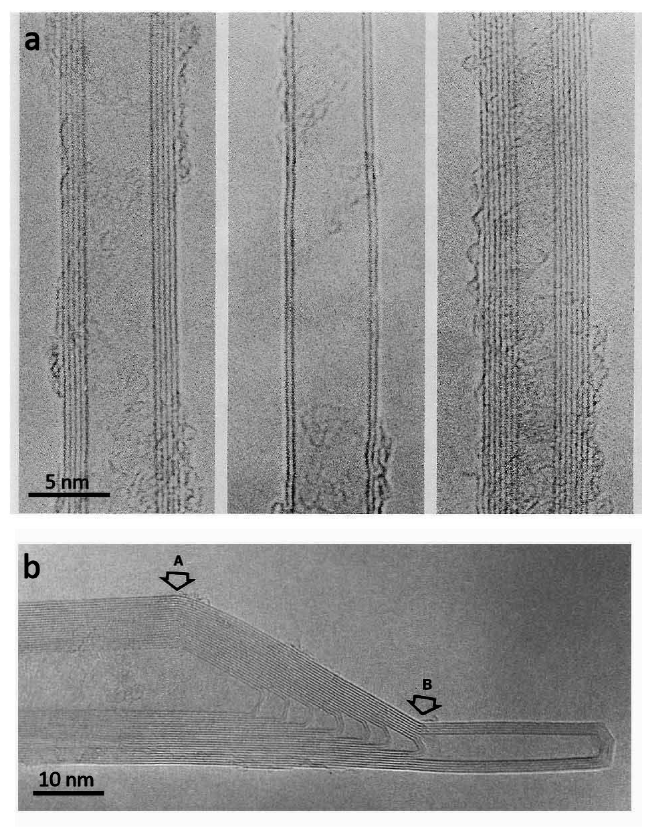
One of the characteristic features of nanotubes produced by arc-evaporation is that they are almost always closed at both ends with caps that can have a variety of structures. In 1992, Iijima and Toshinari Ichihashi published images of caps displaying a “bill-like” morphology, as shown in Figure 4b [51]. In these structures it is believed that a heptagonal ring occurs at the saddle point, labelled “B” in the figure. These images represented the first evidence for 7-membered rings in graphitic materials. In 1993, Iijima’s group and a team led by Donald Bethune at the IBM Almaden Research Center in California independently reported the synthesis of single-walled nanotubes (SWCNTs) [52,53]. These were discovered while carrying out arc-evaporation experiments using graphite electrodes impregnated with metals. This was found to produce single-walled tubes with diameters of the order of 1 nm entangled with amorphous soot and residual particles of metal or metal carbide. Micrographs taken from the Bethune paper are shown in Figure 5. This discovery gave an important boost to nanotube science.
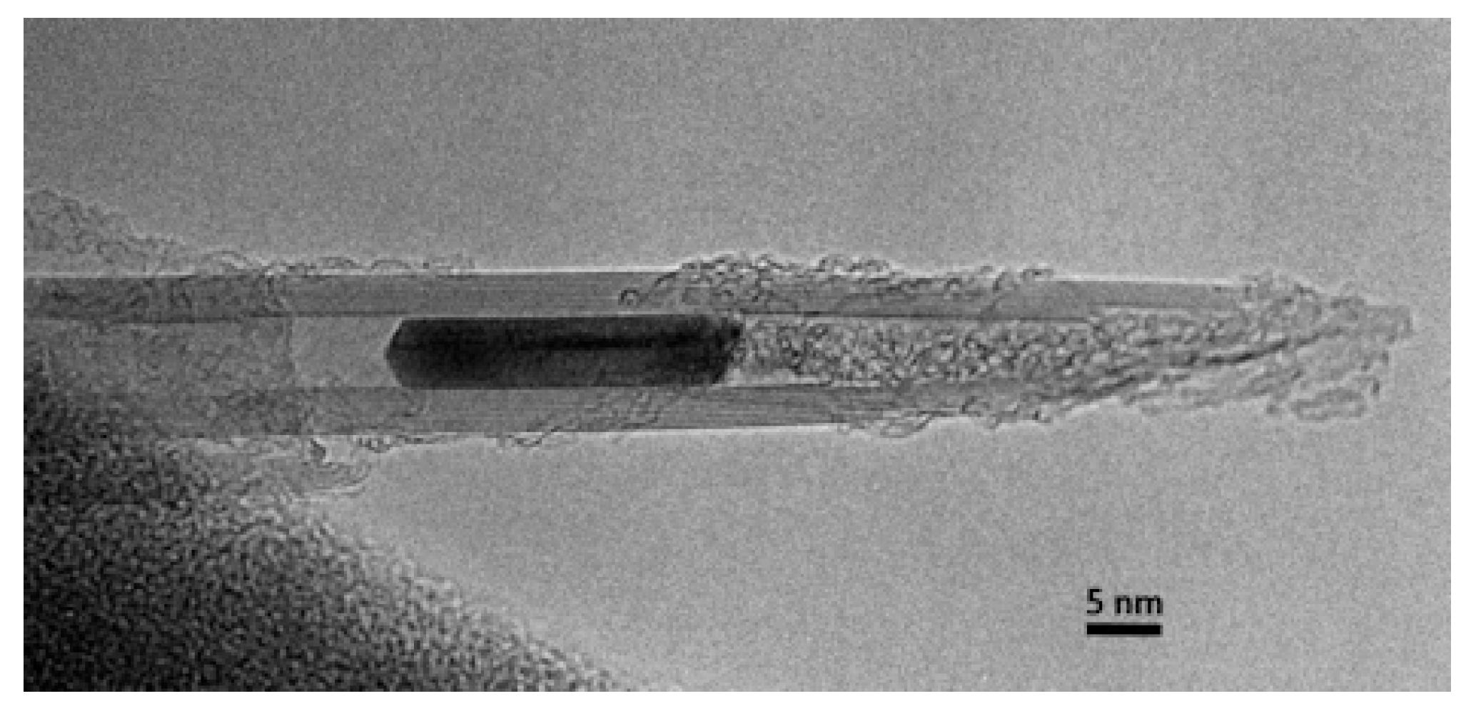
Another very active area of research during the 1990s involved opening and filling carbon nanotubes. The first demonstration of nanotube filling was given by Pulickel Ajayan and Iijima in 1993 [54]. In this work, particles of lead were deposited onto multiwalled tubes in a vacuum and then heated in air at 400 °C, a temperature sufficient to melt the lead. Examination of the resulting material in a TEM showed that small proportion of the tubes had been partially filled. A short time later, more controlled and efficient methods of opening multiwalled nanotubes, using oxidation, were described by Edman Tsang and colleagues (including the present author) at Oxford [55], and by a team led by Ajayan [56]. The Oxford group subsequently showed that MWCNTs could be opened by treating with nitric acid, and that tubes opened in this way could be partially filled with a variety of materials [57]. Figure 6, taken from this work, shows a crystal of metallic nickel inside a multiwalled tube. Jeremy Sloan and colleagues from Oxford showed in 1998 that SCWNTs can be opened and filled using techniques similar to those employed for MCWNTs [58]. At around the same time, Brian Smith, Marc Monthioux, and David Luzzi used a pulsed laser vaporization technique to prepare SCWNTs partially filled with C60 molecules [59]. This remarkable work prompted other groups to explore the encapsulation of larger fullerenes and of metallofullerenes in single-walled tubes (see next section).
Daniel Ugarte, working at the Ecole Polytechnique Fédérale de Lausanne in Switzerland, made an extraordinary discovery in 1992. He found that irradiating carbon nanotubes and nanoparticles with an intense beam of electrons in a TEM caused the structures to evolve into almost perfect spheres apparently made up of concentric fullerenes. In a paper published in Nature [60], Ugarte christened the particles “carbon onions”. They differ from the carbon nanoparticles that accompany nanotubes produced by arc-evaporation: the latter usually have relatively large inner cavities, while onions appear to have a C60 molecule at the centre. Carbon onions should therefore be considered a distinct species of carbon.
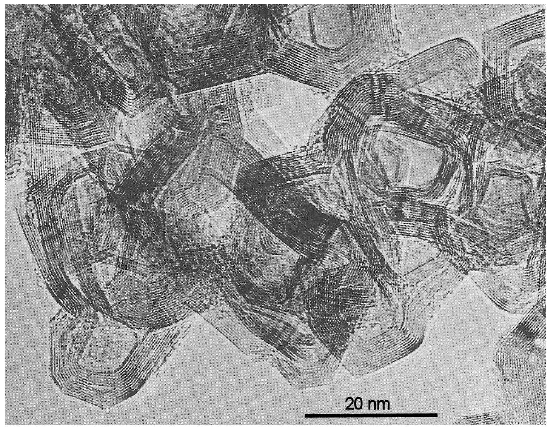
The discovery of fullerenes and of fullerene-related carbons stimulated huge interest. As well as researching the new materials themselves, a number of workers were prompted to take a fresh look at much “older” forms of carbon. In 1997, the present author, with Tsang, published a high resolution TEM study of some non-graphitizing carbons [61]. These are carbons that cannot be transformed into crystalline graphite even at temperatures of 3000 °C and above. They are also known as chars. Their precise structure, and the reasons for their resistance to graphitization, has been a matter of debate since the classic work of Rosalind Franklin in 1951 [62]. In our 1997 work, we showed that heating non-graphitizing carbons to 2600 °C could result in the formation of closed carbon nanoparticles, which were apparently fullerene-like in structure, as shown in Figure 7. Based on these observations, we proposed a new model for the structure of non-graphitizing carbons consisting of curved carbon sheets, in which pentagons and heptagons are dispersed randomly throughout networks of hexagons to create a microporous structure. We believe that this model helps to explain the properties of non-graphitizing carbons, and there is growing evidence that it is correct [63] (see also next section).
Detailed TEM studies of defects in diamond continued into the 1980s. Figure 8 shows a beautiful micrograph of a type Ia diamond, taken from a review of work carried out at Bristol and Oxford in the late 70s and early 80s [64]. This image shows platelets and collapsed platelets. The stripes within the platelets are stacking-fault fringes, which occur because the platelets disrupt the normal stacking sequence in the crystal, creating a diffraction interference effect. The controversy concerning whether the platelets contain nitrogen also continued. In 1982, Steven Berger and Stephen Pennycook of the Cavendish Laboratory, Cambridge, published results obtained using an EELS spectrometer attached to a scanning transmission electron microscope which showed that nitrogen was present [65]. John Bruley and Mick Brown from the same laboratory using the same technique in 1989 found no detectable nitrogen in platelets [66]. Improvements in TEM technology during the 1980s and 1990s meant that lattice imaging of the diamond structure became a practical possibility, and this helped to resolve the nitrogen-in-platelets issue. In 1995, Fallon, Brown, Barry, and Bruley, using a combination of EELS and high-resolution TEM [67], showed that the nitrogen concentration differed from platelet to platelet and concluded that the most likely structure for the platelets was a variation of a model that had been proposed by Humble in 1982 [68]. In this model, the platelets consist of an interstitial layer of carbon atoms pentagonally bonded to the surrounding diamond matrix. The nitrogen is not an essential component of the platelets, but tends to accumulate in the platelets as a result of aggregation of “A centres” (A centres are pairs of nitrogen atoms on adjacent atomic sites in the diamond). Although the precise nature of platelets continues to be debated today, it seems to be generally accepted that the model put forward by Fallon et al. in 1995 is broadly correct.
The nature of voidites was investigated by a number of groups. An edge-on view of a voidite sheet, taken from the review mentioned above [64], is shown in Figure 9. Far from being void, it turned out that these defects are filled with a solid phase. John Hutchison and Leslie Bursill reported in 1983 that the voidites often displayed Moiré patterns [69], and Barry [70] and Hirsch et al. [71] suggested that these were due to the presence of solid nitrogen. Bruley and Brown’s 1989 EELS study confirmed the presence of nitrogen in voidites [66]. Species that would normally be gaseous at room temperature are solid because they experience a high pressure in the voidites. Voidites are believed to form when diamonds containing platelets are subducted to depths of 150 km or so in the continental crust. At these depths, diamonds are metastable and nitrogen is forced out of solid solution. The exsolved nitrogen then forms voidites by displacing carbon atoms [72].
As well as studying defects in natural diamond, Trevor Evans’ group at Reading carried out remarkable work in which the conditions experienced by diamonds in the Earth over millions of years were replicated in the laboratory [73]. This was achieved by placing diamond samples in a specially designed tetrahedral cell, in which they could be subjected to pressures up to 9.5 GPa while being heated to temperatures as high as 2500 °C. When synthetic diamonds containing a high concentration of nitrogen atoms were treated in this way, all the types of aggregate that are found in natural type la diamonds were produced. By analysing the results of these experiments, Evans and colleagues were able to draw conclusions about the conditions experienced by diamonds in the Upper Mantle.
3.4. 2000 to Present
The in-plane carbon-carbon bond distance in graphene is 0.142 nm, too small to be resolved in most conventional TEMs. However, the development of aberration-corrected TEMs meant that the atomic structure of graphene-related carbons could now be directly imaged and, as already noted, this has had a major impact on carbon science. Much of the AC-TEM work on carbon has involved the use of relatively low accelerating voltages (60–80 kV), in order to avoid beam damage. It seems that the first application of aberration-corrected TEM to carbon was a study of single-walled nanotubes by Nobuo Tanaka of Nagoya University [74]. However, the leading figure in this area, at least in the early days, was Kazu Suenaga of Japan’s National Institute for Advanced Industrial Science and Technology. In a series of papers beginning in 2007, Suenaga and his colleagues published images of nanotubes and graphene of a quality that had not been previously seen [75,76,77,78,79,80]. These provided new insights into the nature of defects in SWCNTs [75], the structure of molecules encapsulated inside nanotubes [78], and the edge structure of graphene [79,80]. Figure 10 and Figure 11 show examples of the work of the Suenaga group. In Figure 10, three micrographs are shown, taken a short time apart, of C80 molecules inside a SWCNT [78]. The atomic structures of both the fullerene molecules and the nanotube can be clearly seen, and orientational changes of the fullerene molecules are evident. Figure 11 is taken from a 2010 paper by Suenaga and Masanori Koshino entitled “Atom-by-atom spectroscopy at graphene edge” [80]. Here a low-voltage STEM was used to obtain atomic resolution images of a graphene edge using an annular dark field detector, and to record energy-loss near-edge fine structure (ELNES) spectra of single carbon atoms. In this way, they were able to investigate the electronic and bonding structures of individual edge atoms, a remarkable achievement.
As well as studying nanotubes and graphene, Suenaga’s group, with the present author, recorded the first aberration-corrected TEM images of a microporous carbon in 2008 [81]. The aim of this work was to establish whether evidence could be found to support the idea that these carbons contain pentagons and other non-six-membered rings, in addition to hexagons. Obtaining atomic resolution images of the fresh carbon proved difficult, so samples of carbon heated to 2000 °C were examined. In such samples, clear evidence was found for the presence of pentagonal rings, supporting the view that the carbons have a fullerene-related structure. Junjie Guo et al. reported aberration-corrected TEM images of “fresh” microporous carbons in 2012 [82]. Again, non-six-membered rings were found, but in this case groups of pentagonal and heptagonal carbon rings were seen, rather than isolated pentagons. More studies of this kind on microporous carbons, and other “well-known” forms of carbon would be welcome.
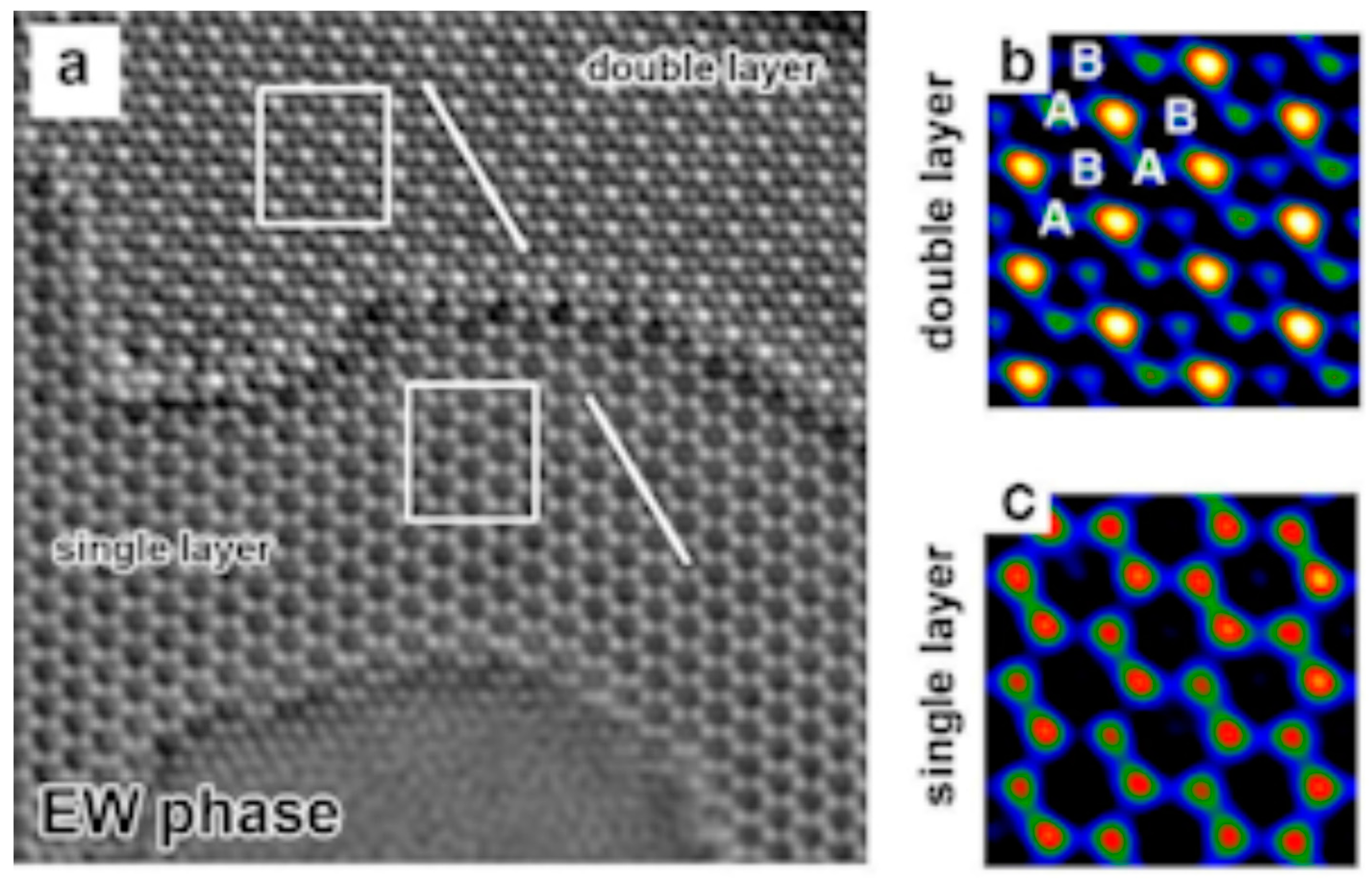
Following the pioneering work of Suenaga and co-workers on the application of aberration-corrected TEM (AC-TEM) to carbon, a number of other groups have carried out exceptional work in this field. Workers from Berkeley using the TEAM (Transmission Electron Aberration-Corrected Microscope) have published beautiful images of defects and edge structures in graphene [83,84], and Jannik Meyer, who was a member of the Berkeley group, has continued to study graphene using AC-TEM at the University of Vienna [85,86]. Jamie Warner and co-workers at Oxford have conducted a comprehensive analysis of defects in single-layer and bilayer graphene [87,88,89,90], while the Manchester group [91] and the SuperSTEM team at Daresbury [92] have studied a range of 2-dimensional materials and heterostructures, as well as graphene. Three-dimensional forms of graphene have also been investigated by the present author in partnership with the Manchester and SuperSTEM microscopists [93]. Joerg Jinschek of the FEI Company and co-workers used the technique of exit-wave reconstruction to obtain extremely high quality images of graphene using an AC-TEM at 80 kV [94]. Exit-wave reconstruction involves extracting the wave function at the exit surface of the specimen, with aberrations and incoherence due to the imaging optics removed. Jinschek et al. applied this method to a through focal series of micrographs of a region containing single-layer and bilayer graphene to produce the superb image shown in Figure 12.
If imaging graphene using aberration-corrected TEM presents a challenge [95], then obtaining AC-TEM images of diamond is even more demanding. Whereas graphene is naturally just one atomic layer thick, bulk diamond has to be thinned down to a thickness of less than 50 nm in order to obtain interpretable images, and this is a non-trivial task. One of the few AC-TEM studies of bulk natural diamond was carried out by Iain Godfrey and Ursel Bangert at Manchester [96]. Aberration-corrected STEM imaging and EELS were used to investigate the factors that determine their colour, with a particular focus on vacancy clusters. Unlike natural diamond, synthetic diamond produced by chemical vapor deposition (CVD) is relatively amenable to TEM study. It can be deposited as a thin film and then further thinned using ion milling to produce electron-transparent specimens. In 2006, an international group led by Rolf Erni used an aberration-corrected STEM to resolve the 0.089 nm “dumbbell” distance in the <110> zone axis orientation of CVD diamond [97]. A Japanese group, including Suenaga, Hidetaka Sawada, and Kunio Takayanagi, recorded a similar image, shown in Figure 13, using an aberration-corrected TEM in 2013 [98]. These images provide a vivid demonstration of the resolving power of this new generation of microscopes.
4. Discussion
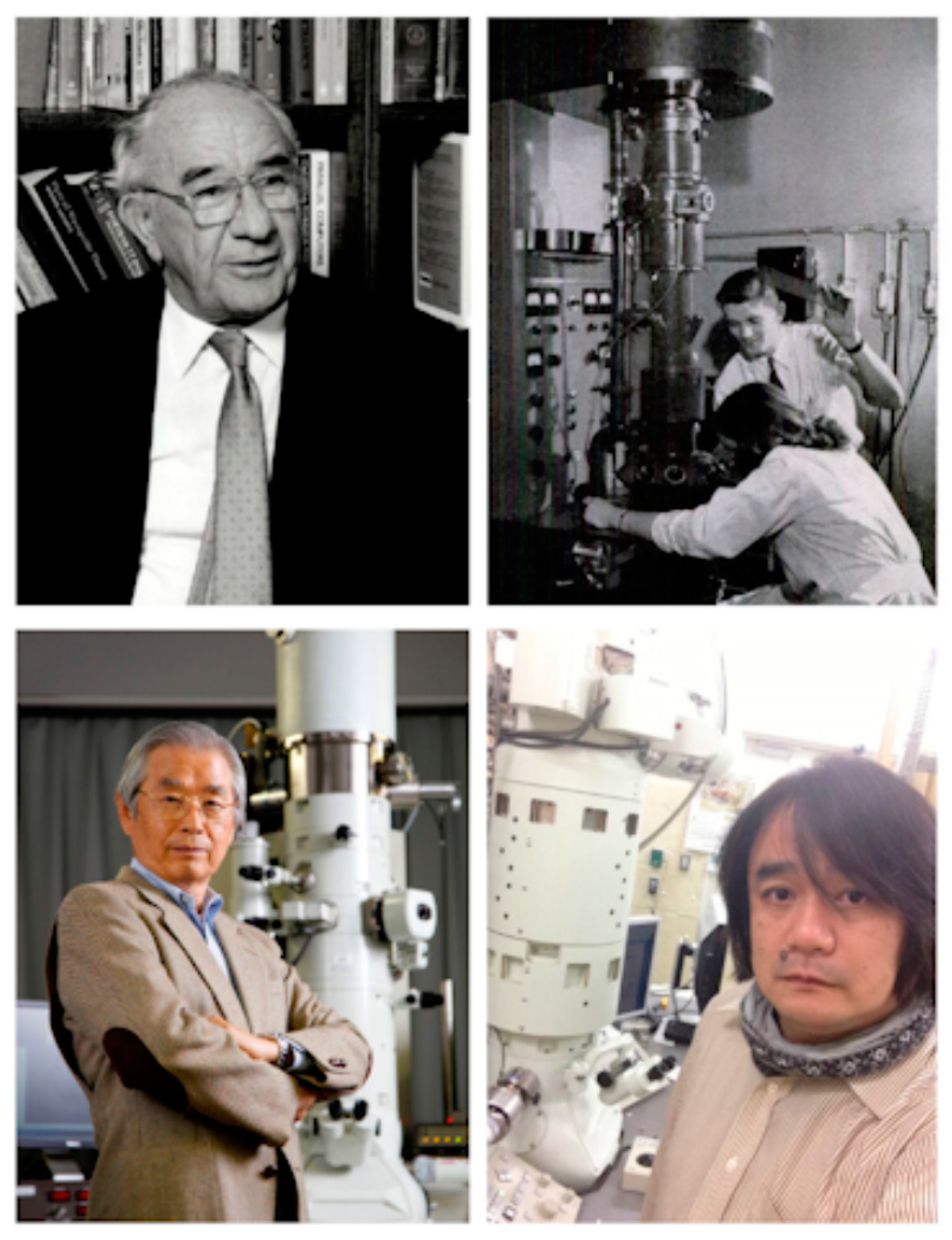
In the past 70 years, transmission electron microscopy of carbon has advanced from low resolution imaging of carbon black particles to recording images and spectra from individual atoms. These amazing advances have been made possible by the skill and dedication of many outstanding scientists. Some of the leading figures in the field are shown in Figure 14. Trevor Evans of Reading University was the first to study diamond by TEM, and his group was responsible for recording the first images of platelets and voidites. Reading remained at the forefront of TEM studies of diamond for many years, together with workers from Oxford, including Peter Hirsch, John Barry, John Bruley, and John Hutchison, and Mick Brown and colleagues from Cambridge. These researchers pushed against the limits of the technology available at the time to eventually establish the true nature of the defects that had been first observed at Reading in the early 1960s.
Robert Heidenreich of Bell Labs was a pioneer in the application of TEM to metals, and made a very significant contribution to the study of carbon by recording the first lattice images of graphitized carbon black in 1968. In Heidenreich’s work, the carbon black was intended to be a “test object” for high resolution TEM, but the demonstration that graphite planes could be directly imaged opened the way for a massive expansion of TEM studies of sp2 carbon in all its forms. This led to many important advances in our understanding of graphite, glassy carbon, carbon black, carbon fibres, and catalytically grown carbon filaments.
Sumio Iijima of the NEC Corporation is best known for the discovery of a completely new form of carbon filaments—fullerene-related carbon nanotubes—in 1991, but he had been a leading figure in electron microscopy since the early 1970s, making important contributions to the study of complex oxides and ultra-fine metal particles. Since 1991, he has concentrated most of his research effort on carbon nanotubes, carbon nanohorns, and graphene, and continues to publish papers on TEM of carbon to this day. Kazu Suenaga of AIST in Tsukuba, who has worked closely with Iijima, led the way in the application of aberration-corrected TEM to carbon, recording some of the first truly atomic resolution images of carbon nanotubes and graphene. The development of these new super-high resolution microscopes has represented a quantum leap in carbon imaging and fortuitously coincided with the discovery of graphene; much of what we now know about defect structures in graphene has been obtained by the application of AC-TEM. Carbon science has seen some extraordinary advances in recent years. However the field develops in the future, it seems certain that TEM will continue to play a central role.
Acknowledgments
I am grateful to Chris Ewels, Malcolm Heggie, Fredrik Hage, Jon Goss, Kazu Suenaga, and Hidetaka Sawada for helpful discussions and comments. Special thanks go to John Barry for helping to guide me through the complexities of defects in diamond.
Conflicts of Interest
The author declares no conflict of interest.
References
- Ruska, E.; Knoll, M. Das Elektronenmikroskop. Z. Phys. 1932, 78, 318–339. [Google Scholar]
- Scherzer, O. Über einige Fehler von Elektronenlinsen. Z. Phys. 1936, 101, 593–603. [Google Scholar] [CrossRef]
- Heidenreich, R.D. Electron microscope and diffraction study of metal crystal textures by means of thin sections. J. Appl. Phys. 1949, 20, 993–1010. [Google Scholar] [CrossRef]
- Hirsch, P.B.; Horne, R.W.; Whelan, M.J. Direct observations of the arrangement and motion of dislocations in aluminium. Philos. Mag. 1956, 1, 677–684. [Google Scholar] [CrossRef]
- Bollmann, W. Interference effects in the electron microscopy of thin crystal foils. Phys. Rev. 1956, 103, 1588–1589. [Google Scholar] [CrossRef]
- Menter, J.W. The direct study by electron microscopy of crystal lattices and their imperfections. Proc. R. Soc. A 1956, 236, 119–135. [Google Scholar] [CrossRef]
- Suito, E.; Uyeda, N.; Watanabe, H.; Komoda, T. Lattice image of twin structure observed directly by electron microscope in a crystal of copper phthalocyanine. Nature 1958, 181, 332–333. [Google Scholar] [CrossRef]
- Komoda, T. Observation of lattice planes of 2.35 Å spacing with an electron microscope. Jpn. J. Appl. Phys. 1966, 3, 122–123. [Google Scholar] [CrossRef]
- Heidenreich, R.D.; Hess, W.M.; Ban, L.L. A test object and criteria for high resolution electron microscopy. J. Appl. Crystallogr. 1968, 1, 1–19. [Google Scholar] [CrossRef]
- Von Ardenne, M. Das elektronen-rastermikroskop. Theoretische grundlagen. Z. Phys. 1938, 109, 553–572. [Google Scholar] [CrossRef]
- Crewe, A.V.; Wall, J.; Langmore, J. Visibility of single atoms. Science 1970, 168, 1338–1340. [Google Scholar] [CrossRef] [PubMed]
- Brydson, R. Electron Energy Loss Spectroscopy; Taylor & Francis: London, UK, 2001. [Google Scholar]
- Haider, M.; Rose, H.; Uhlemann, S.; Schwan, E.; Kabius, B.; Urban, K. Towards 0.1 nm resolution with the first spherically corrected transmission electron microscope. J. Electron Microsc. 1998, 47, 395–405. [Google Scholar] [CrossRef]
- Hawkes, P.W. The Beginnings of Electron Microscopy; Academic Press: Orlando, FL, USA, 1985. [Google Scholar]
- Braun, E. Mechanical properties of solids. In Out of the Crystal Maze: Chapters from the History of Solid-State Physics; Hoddeson, L., Braun, E., Teichmann, J., Weart, S., Eds.; Oxford University Press: Oxford, UK, 1991; pp. 317–358. [Google Scholar]
- Hirsch, P.B. Electron microscopy in materials science a historical perspective. In The Electron: Proceedings of the International Centennial Symposium on the Electron; Kirkland, A.I., Brown, P.D., Eds.; IOM Communications: London, UK, 1998; pp. 64–81. [Google Scholar]
- Rose, H.H. Historical aspects of aberration correction. J. Electron Microsc. 2009, 58, 77–85. [Google Scholar] [CrossRef] [PubMed]
- Zhang, B.; Su, D.S. Transmission electron microscopy and the science of carbon nanomaterials. Small 2014, 10, 222–229. [Google Scholar] [CrossRef] [PubMed]
- Hofmann, U.; Höper, W. On the “active sites” in catalysis (in German). Naturwissenschaften 1944, 32, 225–226. [Google Scholar] [CrossRef]
- Watson, J.H.L. Filmless sample mounting for the electron microscope. J. Appl. Phys. 1946, 17, 121–127. [Google Scholar] [CrossRef]
- Hall, C.E. Dark-field electron microscopy: II. Studies of colloidal carbon. J. Appl. Phys. 1948, 19, 271–277. [Google Scholar] [CrossRef]
- Radushkevich, L.V.; Lukyanovich, V.M. On the carbon structure formed during thermal decomposition of carbon monoxide in the presence of iron (in Russian). Zhurnal Fizicheskoi Khimii 1952, 26, 88–95. [Google Scholar]
- Monthioux, M.; Kuznetsov, V.L. Who should be given the credit for the discovery of carbon nanotubes? Carbon 2006, 44, 1621–1623. [Google Scholar] [CrossRef]
- Davis, W.; Slawson, R.; Rigby, G.R. An unusual form of carbon. Nature 1953, 171, 756. [Google Scholar] [CrossRef]
- Bacon, R. Growth, structure and properties of graphite whiskers. J. Appl. Phys. 1960, 31, 283–290. [Google Scholar] [CrossRef]
- Bollmann, W. Electron-microscopic observations on radiation damage in graphite. Philos. Mag. 1960, 5, 621–624. [Google Scholar] [CrossRef]
- Jenkins, G.M.; Turnbull, J.A.; Williamson, G.K. Electron microscope studies of graphitization and deformation in carbon film. J. Nucl. Mater. 1962, 7, 215–217. [Google Scholar] [CrossRef]
- Jenkins, G.M.; Williamson, G.K.; Barnett, J.T. The role of crystal structure in determining the mechanical properties of graphite. Carbon 1965, 3, 1–6. [Google Scholar] [CrossRef]
- Amelinckx, S.; Delavignette, P.; Heerschap, M. Dislocations and stacking faults in graphite. Chem. Phys. Carbon 1965, 1, 1–71. [Google Scholar]
- Thrower, P.A. The study of defects in graphite by transmission electron microscopy. Chem. Phys. Carbon 1969, 5, 217–319. [Google Scholar]
- Thomas, J.M. Microscopic studies of graphite oxidation. Chem. Phys. Carbon 1966, 1, 122–202. [Google Scholar]
- Evans, E.L.; Griffiths, R.J.M.; Thomas, J.M. Kinetics of single-layer graphite oxidation: Evaluation by electron microscopy. Science 1971, 171, 174–175. [Google Scholar] [CrossRef] [PubMed]
- Baker, R.T.K.; Harris, P.S. The formation of filamentous carbon. Chem. Phys. Carbon 1978, 14, 83–165. [Google Scholar]
- Marton, L.L. La microscopie électronique des objets biologiques. Bull. Acad. R. Med. Belg. 1935, 21, 553–564. [Google Scholar]
- Endo, M. Grow carbon-fibers in the vapor-phase. Chemtech 1988, 18, 568–576. [Google Scholar]
- Ban, L.L. Direct study of structural imperfections by high-resolution electron microscopy. In Surface and Defect Properties of Solids; Roberts, M.W., Thomas, J.M., Eds.; Chemical Society: London, UK, 1972; Volume 1, pp. 54–94. [Google Scholar]
- Crawford, D.; Johnson, D.J. High-resolution electron microscopy of high-modulus carbon fibres. J. Microsc. 1971, 94, 51–62. [Google Scholar] [CrossRef]
- Jenkins, G.M.; Kawamura, K. Structure of glassy carbon. Nature 1971, 231, 175–176. [Google Scholar] [CrossRef] [PubMed]
- Ban, L.L.; Crawford, D.; Marsh, H. Lattice-resolution electron-microscopy in structural studies of non-graphitizing carbons from polyvinylidene chloride (PVDC). J. Appl. Crystallogr. 1975, 8, 415–420. [Google Scholar] [CrossRef]
- Oberlin, A.; Terriere, G. Graphitization studies of anthracites by high-resolution electron-microscopy. Carbon 1975, 13, 367–376. [Google Scholar] [CrossRef]
- Crawford, D.; Marsh, H. High resolution electron microscopy of carbon structure. J. Microsc. 1977, 109, 145–152. [Google Scholar] [CrossRef]
- Millward, G.R.; Jefferson, D.A. Lattice resolution of carbons by electron microscopy. Chem. Phys. Carbon 1978, 14, 1–82. [Google Scholar]
- Evans, T.; Phaal, C. Imperfections in type I and type II diamonds. Proc. R. Soc. A 1962, 270, 538–552. [Google Scholar] [CrossRef]
- Frank, F.C. On the X-ray diffraction spikes of diamond. Proc. R. Soc. A 1956, 237, 168–174. [Google Scholar] [CrossRef]
- Lang, A.R. A proposed structure for nitrogen impurity platelets in diamond. Proc. Phys. Soc. Lond. 1964, 84, 871–876. [Google Scholar] [CrossRef]
- Woods, G.S. Electron microscopy of ‘giant’ platelets on cube planes in diamond. Philos. Mag. A 1976, 34, 993–1012. [Google Scholar] [CrossRef]
- Stephenson, R.F. The Partial Dissociation of Nitrogen Aggregates in Diamond by High Temperature-High Pressure Treatments. Ph.D. Thesis, University of Reading, Reading, UK, 1978. [Google Scholar]
- Kroto, H.W.; Heath, J.R.; O’Brien, S.C.; Curl, R.F.; Smalley, R.E. C60: Buckminsterfullerene. Nature 1985, 318, 162–163. [Google Scholar] [CrossRef]
- Iijima, S. Helical microtubules of graphitic carbon. Nature 1991, 354, 56–58. [Google Scholar] [CrossRef]
- Krätschmer, W.; Lamb, L.D.; Fostiropoulos, K.; Huffman, D.R. Solid C60: A new form of carbon. Nature 1990, 347, 354–358. [Google Scholar] [CrossRef]
- lijima, S.; Ichihashi, T.; Ando, Y. Pentagons, heptagons and negative curvature in graphite microtubule growth. Nature 1992, 356, 776–778. [Google Scholar] [CrossRef]
- Iijima, S.; Ichihashi, T. Single-shell carbon nanotubes of 1-nm diameter. Nature 1993, 363, 603–605. [Google Scholar] [CrossRef]
- Bethune, D.S.; Kiang, C.H.; de Vries, M.S.; Gorman, G.; Savoy, R.; Vazquez, J.; Beyers, R. Cobalt-catalysed growth of carbon nanotubes with single-atomic-layer walls. Nature 1993, 363, 605–607. [Google Scholar] [CrossRef]
- Ajayan, P.M.; Iijima, S. Capillarity-induced filling of carbon nanotubes. Nature 1993, 361, 333–334. [Google Scholar] [CrossRef]
- Tsang, S.C.; Harris, P.J.F.; Green, M.L.H. Thinning and opening of carbon nanotubes by oxidation using carbon dioxide. Nature 1993, 362, 520–522. [Google Scholar] [CrossRef]
- Ajayan, P.M.; Ebbesen, T.W.; Ichihashi, T.; Iijima, S.; Tanigaki, K.; Hiura, H. Opening carbon nanotubes with oxygen and implications for filling. Nature 1993, 362, 522–525. [Google Scholar] [CrossRef]
- Tsang, S.C.; Chen, Y.K.; Harris, P.J.F.; Green, M.L.H. A simple chemical method of opening and filling carbon nanotubes. Nature 1994, 372, 159–162. [Google Scholar] [CrossRef]
- Sloan, J.; Hammer, J.; Zwiefka-Sibley, M.; Green, M.L.H. The opening and filling of single walled carbon nanotubes (SWTs). Chem. Commun. 1998, 3, 347–348. [Google Scholar] [CrossRef]
- Smith, B.W.; Monthioux, M.; Luzzi, D.E. Encapsulated C60 in carbon nanotubes. Nature 1998, 396, 323–324. [Google Scholar] [CrossRef]
- Ugarte, D. Curling and closure of graphitic networks under electron-beam irradiation. Nature 1992, 359, 707–709. [Google Scholar] [CrossRef] [PubMed]
- Harris, P.J.F.; Tsang, S.C. High-resolution electron microscopy studies of non-graphitizing carbons. Philos. Mag. A 1997, 76, 667–677. [Google Scholar] [CrossRef]
- Franklin, R.E. Crystallite growth in graphitizing and non-graphitizing carbons. Proc. R. Soc. A 1951, 209, 196–218. [Google Scholar] [CrossRef]
- Harris, P.J.F. Fullerene-like models for microporous carbon. J. Mater. Sci. 2013, 48, 565–577. [Google Scholar] [CrossRef]
- Barry, J.C.; Bursill, L.A.; Hutchison, J.L.; Lang, A.R.; Rackham, G.M.; Sumida, N. On voidites: A high-resolution transmission electron microscopic study of faceted void-like defects in natural diamonds. Philos. Trans. R. Soc. Lond. Ser. A 1987, 321, 361–401. [Google Scholar] [CrossRef]
- Berger, S.D.; Pennycook, S.J. Detection of nitrogen at {100} platelets in diamond. Nature 1982, 298, 635–637. [Google Scholar] [CrossRef]
- Bruley, J.; Brown, L.M. Quantitative electron energy-loss spectroscopy microanalysis of platelet and voidite defects in natural diamond. Philos. Mag. A 1989, 59, 247–261. [Google Scholar] [CrossRef]
- Fallon, P.J.; Brown, L.M.; Barry, J.C.; Bruley, J. Nitrogen determination and characterization in natural diamond platelets. Philos. Mag. A 1995, 72, 21–37. [Google Scholar] [CrossRef]
- Humble, P. The structure and mechanism of formation of platelets in natural type Ia diamond. Proc. R. Soc. A 1982, 381, 65–81. [Google Scholar] [CrossRef]
- Hutchison, J.L.; Bursill, L.A. Fresnel fringe contrast of faceted voids within gem-quality diamond. J. Microsc. 1983, 131, 63–66. [Google Scholar] [CrossRef]
- Barry, J.C. Voidites in diamond—Do they contain nitrogen? Ultramicroscopy 1986, 20, 169–176. [Google Scholar] [CrossRef]
- Hirsch, P.B.; Hutchison, J.L.; Titchmarsh, J. Voidites in diamond: Evidence for a crystalline phase containing nitrogen. Philos. Mag. A 1986, 54, L49–L54. [Google Scholar] [CrossRef]
- Barry, J.C.; Queensland University of Technology, Brisbane, Australia. Personal communication, 2017.
- Evans, T.; Qi, Z. The kinetics of the aggregation of nitrogen atoms in diamond. Proc. R. Soc. A 1982, 381, 159–178. [Google Scholar] [CrossRef]
- Hirahara, K.; Saitoh, K.; Yamasaki, J.; Tanaka, N. Direct observation of six-membered rings in the upper and lower walls of a single-wall carbon nanotube by spherical aberration-corrected HRTEM. Nano Lett. 2006, 6, 1778–1783. [Google Scholar] [CrossRef] [PubMed]
- Suenaga, K.; Wakabayashi, H.; Koshino, M.; Sato, Y.; Urita, K.; Iijima, S. Imaging active topological defects in carbon nanotubes. Nat. Nanotechnol. 2007, 2, 358–360. [Google Scholar] [CrossRef] [PubMed]
- Guan, L.; Suenaga, K.; Iijima, S. Smallest carbon nanotube assigned with atomic resolution accuracy. Nano Lett. 2008, 8, 459–462. [Google Scholar] [CrossRef] [PubMed]
- Sato, Y.; Yanagi, K.; Miyata, Y.; Suenaga, K.; Kataura, H.; Iijima, S. Chiral-angle distribution for separated single-walled carbon nanotubes. Nano Lett. 2008, 8, 3151–3154. [Google Scholar] [CrossRef] [PubMed]
- Sato, Y.; Suenaga, K.; Okubo, S.; Okazaki, T.; Iijima, S. Structures of D5d-C80 and Ih-Er3N@C80 Fullerenes and Their Rotation Inside Carbon Nanotubes Demonstrated by Aberration-Corrected Electron Microscopy. Nano Lett. 2007, 7, 3704–3708. [Google Scholar] [CrossRef]
- Liu, Z.; Suenaga, K.; Harris, P.J.F.; Iijima, S. Open and closed edges of graphene layers. Phys. Rev. Lett. 2009, 102, 015501. [Google Scholar] [CrossRef] [PubMed]
- Suenaga, K.; Koshino, M. Atom-by-atom spectroscopy at graphene edge. Nature 2010, 468, 1088–1090. [Google Scholar] [CrossRef] [PubMed]
- Harris, P.J.F.; Liu, Z.; Suenaga, K. Imaging the atomic structure of activated carbon. J. Phys. Condens. Matter 2008, 20, 362201. [Google Scholar] [CrossRef]
- Guo, J.; Morris, J.R.; Ihm, Y.; Contescu, C.I.; Gallego, N.C.; Duscher, G.; Pennycook, S.J.; Chisholm, M.F. Topological defects: Origin of nanopores and enhanced adsorption performance in nanoporous carbon. Small 2012, 8, 3283–3288. [Google Scholar] [CrossRef] [PubMed]
- Meyer, J.C.; Kisielowski, C.; Erni, R.; Rossell, M.D.; Crommie, M.F.; Zettl, A. Direct imaging of lattice atoms and topological defects in graphene membranes. Nano Lett. 2008, 8, 3582–3586. [Google Scholar] [CrossRef] [PubMed]
- Girit, Ç.Ö.; Meyer, J.C.; Erni, R.; Rossell, M.D.; Kisielowski, C.; Yang, L.; Park, C.-H.; Crommie, M.F.; Cohen, M.L.; Louie, S.G.; et al. Graphene at the edge: Stability and dynamics. Science 2009, 323, 1705–1708. [Google Scholar] [CrossRef] [PubMed]
- Meyer, J.C.; Kotakoski, J.; Mangler, C. Atomic structure from large-area, low-dose exposures of materials: A new route to circumvent radiation damage. Ultramicroscopy 2014, 145, 13–21. [Google Scholar] [CrossRef] [PubMed]
- Kotakoski, J.; Mangler, C.; Meyer, J.C. Imaging atomic-level random walk of a point defect in graphene. Nat. Commun. 2014, 5, 3991. [Google Scholar] [CrossRef] [PubMed]
- Warner, J.H.; Ruemmeli, M.H.; Gemming, T.; Buechner, B.; Briggs, G.A.D. Direct imaging of rotational stacking faults in few layer graphene. Nano Lett. 2009, 9, 102–106. [Google Scholar] [CrossRef] [PubMed]
- Warner, J.H.; Margine, E.R.; Mukai, M.; Robertson, A.W.; Giustino, F.; Kirkland, A.I. Dislocation-driven deformations in graphene. Science 2012, 337, 209–212. [Google Scholar] [CrossRef] [PubMed]
- Robertson, A.W.; Allen, C.S.; Wu, Y.A.; He, K.; Olivier, J.; Neethling, J.; Kirkland, A.I.; Warner, J.H. Spatial control of defect creation in graphene at the nanoscale. Nat. Commun. 2012, 3, 1144. [Google Scholar] [CrossRef] [PubMed]
- Gong, C.; Lee, S.; Hong, S.; Yoon, E.; Lee, G.D.; Warner, J.H. Point defects in turbostratic stacked bilayer grapheme. Nanoscale 2017, 9, 13725–13730. [Google Scholar] [CrossRef] [PubMed]
- Haigh, S.J.; Gholinia, A.; Jalil, R.; Romani, S.; Britnell, L.; Elias, D.C.; Novoselov, K.S.; Ponomarenko, L.A.; Geim, A.K.; Gorbachev, R. Cross-sectional imaging of individual layers and buried interfaces of graphene-based heterostructures and superlattices. Nat. Mater. 2012, 11, 764–767. [Google Scholar] [CrossRef] [PubMed]
- Zan, R.; Ramasse, Q.M.; Jalil, R.; Tu, J.-S.; Bangert, U.; Novoselov, K.S. Imaging two dimensional materials and their heterostructures. J. Phys. Conf. Ser. 2017, 902, 012028. [Google Scholar] [CrossRef]
- Harris, P.J.F.; Slater, T.J.A.; Haigh, S.J.; Hage, F.S.; Kepaptsoglou, D.M.; Ramasse, Q.M.; Brydson, R. Bilayer graphene formed by passage of current through graphite: Evidence for a three-dimensional structure. Nanotechnology 2014, 25, 465601. [Google Scholar] [CrossRef] [PubMed]
- Jinschek, J.R.; Yucelen, E.; Calderon, H.A.; Freitag, B. Quantitative atomic 3-D imaging of single/double sheet graphene structure. Carbon 2011, 49, 556–562. [Google Scholar] [CrossRef]
- Urban, K.W. Electron microscopy: The challenges of graphene. Nat. Mater. 2011, 10, 165–166. [Google Scholar] [CrossRef] [PubMed]
- Godfrey, I.S.; Bangert, U. An analysis of vacancy clusters and sp2 bonding in natural type IIa diamond using aberration corrected STEM and EELS. J. Phys. Conf. Ser. 2011, 281, 012024. [Google Scholar] [CrossRef]
- Erni, R.; Freitag, B.; Hartel, P.; Müller, H.; Tiemeijer, P.; van der Stam, M.; Stekelenburg, M.; Hubert, D.; Specht, P.; Garibay-Febles, V. Atomic scale analysis of planar defects in polycrystalline diamond. Microsc. Microanal. 2006, 12, 492–497. [Google Scholar] [CrossRef] [PubMed]
- Hosokawa, F.; Sawada, H.; Kondo, Y.; Takayanagi, K.; Suenaga, K. Development of Cs and Cc correctors for transmission electron microscopy. Microscopy 2013, 62, 23–41. [Google Scholar] [CrossRef] [PubMed]
Figure 1.
Very early transmission electron microscopy images of hollow carbon filaments. Reproduced with permission from [22]. Nauka Publishers, 1952.
Figure 1.
Very early transmission electron microscopy images of hollow carbon filaments. Reproduced with permission from [22]. Nauka Publishers, 1952.

Figure 2.
Early lattice image of carbon black, by Ban. Reproduced with permission from [36]. Royal Society of Chemistry, 1972.
Figure 2.
Early lattice image of carbon black, by Ban. Reproduced with permission from [36]. Royal Society of Chemistry, 1972.

Figure 3.
One of the first TEM images of platelets in type Ia diamond, from a 1962 paper by Evans & Phaal. Reproduced with permission from [43]. Royal Society, 1962.
Figure 3.
One of the first TEM images of platelets in type Ia diamond, from a 1962 paper by Evans & Phaal. Reproduced with permission from [43]. Royal Society, 1962.

Figure 4.
(a) Some of Iijima’s first images of multiwalled nanotubes. Reproduced with permission from [49]. Springer Nature, 1991; (b) Multiwalled nanotube cap. “A” indicates position of single pentagon; “B” indicates probable position of single heptagon. Reproduced with permission from [51]. Springer Nature, 1992.

Figure 5.
Images from the work of Bethune et al. showing single-walled carbon nanotubes produced by co-vaporization of graphite and cobalt. Reproduced with permission from [53]. Springer Nature, 1993.
Figure 5.
Images from the work of Bethune et al. showing single-walled carbon nanotubes produced by co-vaporization of graphite and cobalt. Reproduced with permission from [53]. Springer Nature, 1993.
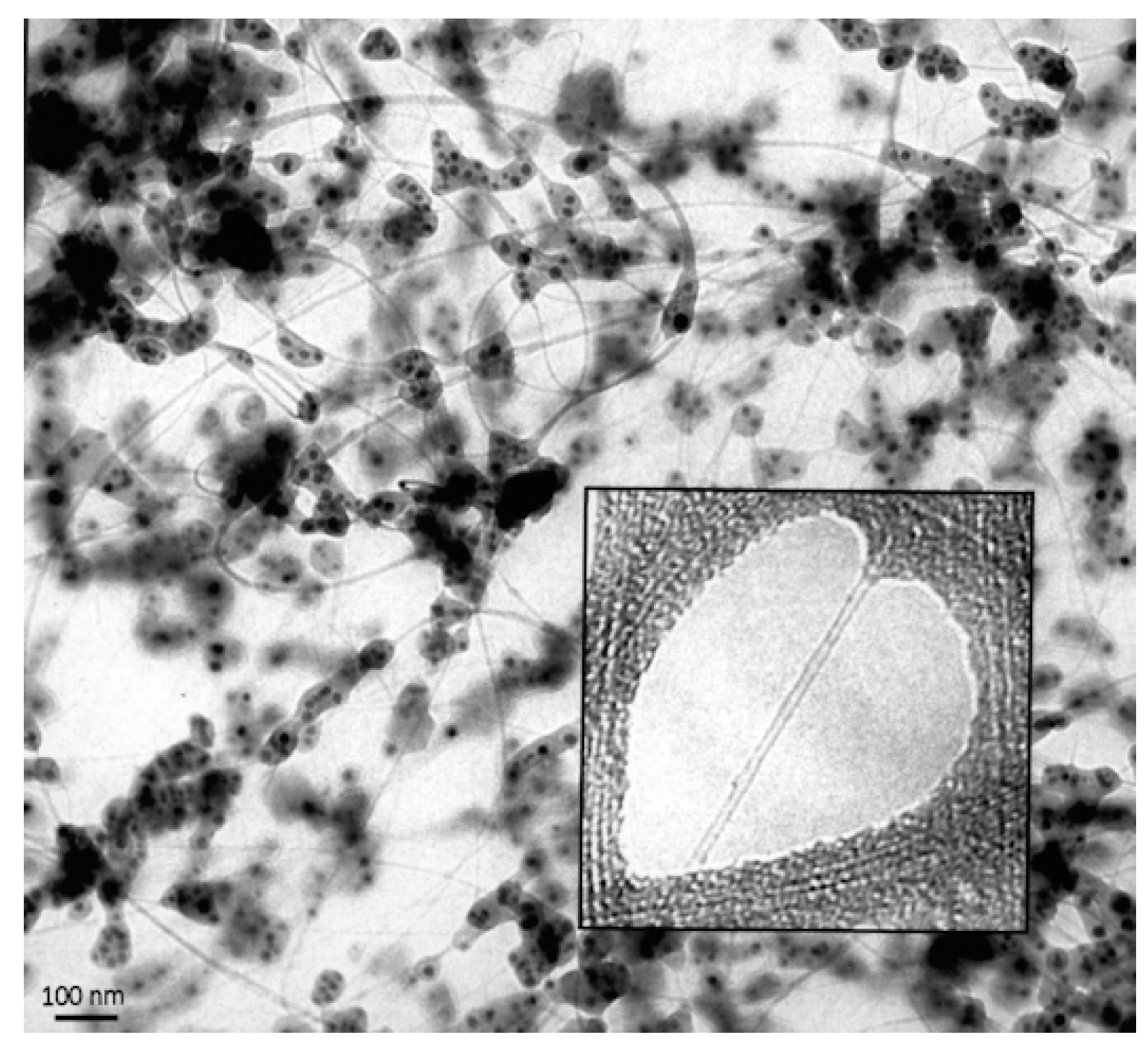
Figure 6.
Nanotube partially filled with metallic nickel prepared by hydrogen reduction of a NiO precursor. Reproduced with permission from [57]. Springer Nature, 1994.
Figure 6.
Nanotube partially filled with metallic nickel prepared by hydrogen reduction of a NiO precursor. Reproduced with permission from [57]. Springer Nature, 1994.

Figure 7.
(a) Micrograph showing closed structure in polyvinylidene chloride (PVDC)-derived carbon heated at 2600 °C; (b) another micrograph of same sample, with arrows showing regions of negative curvature. From work by Harris and Tsang. Reproduced with permission from [61]. Taylor & Francis, 1997.
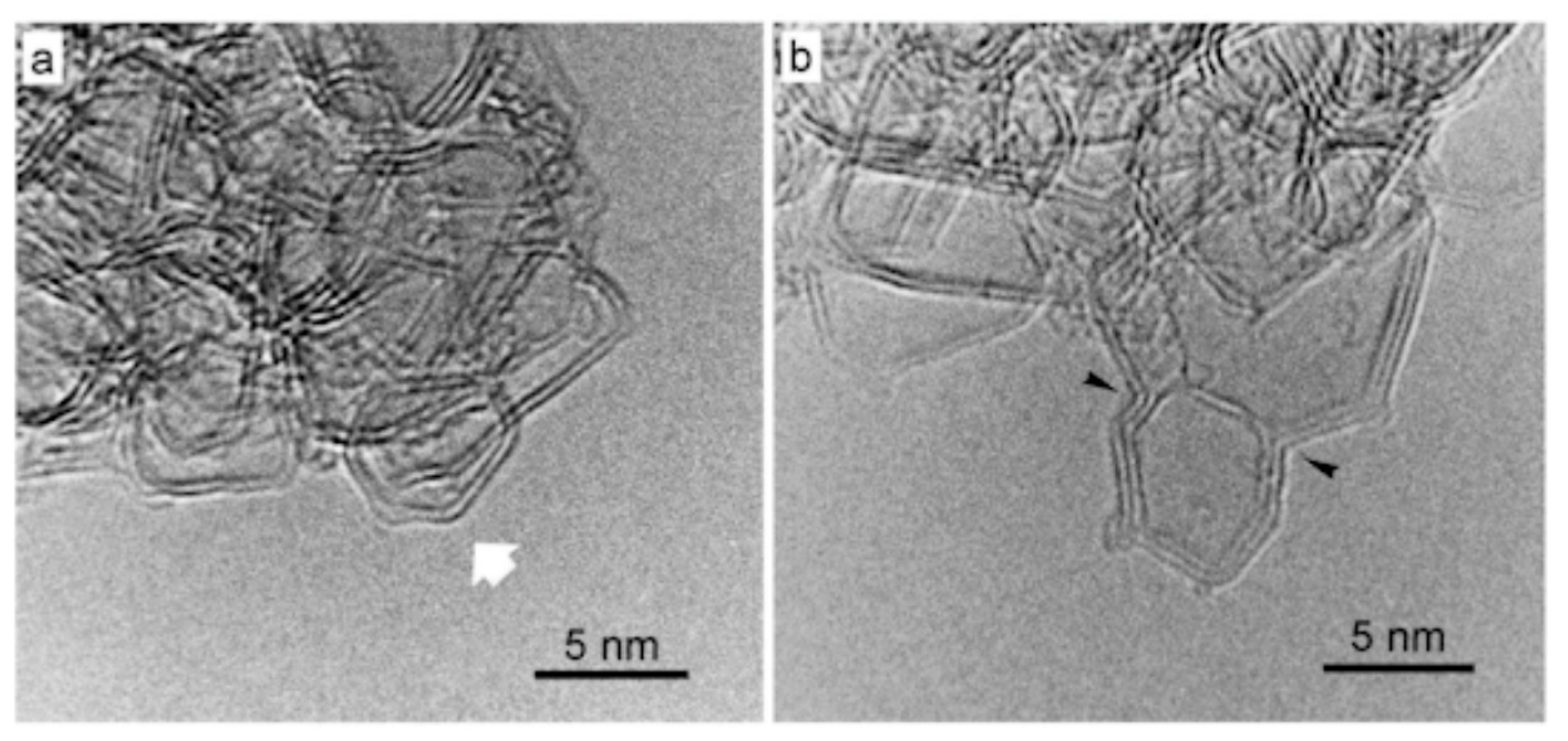
Figure 8.
Image of type Ia diamond from work by Barry et al. showing large platelets. Reproduced with permission from [64]. Royal Society, 1987.
Figure 8.
Image of type Ia diamond from work by Barry et al. showing large platelets. Reproduced with permission from [64]. Royal Society, 1987.

Figure 9.
Voidite sheet in type Ia diamond. Reproduced with permission from [64]. Royal Society, 1987.
Figure 9.
Voidite sheet in type Ia diamond. Reproduced with permission from [64]. Royal Society, 1987.
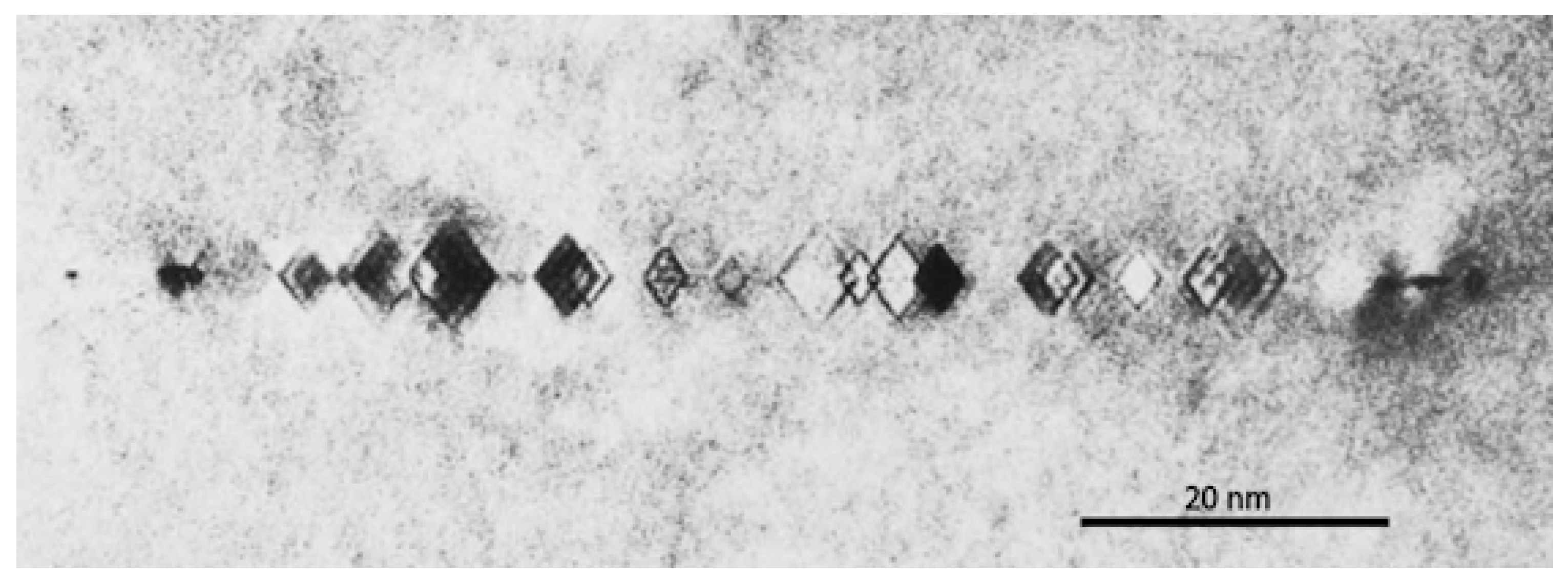
Figure 10.
Aberration-corrected TEM images of D5d-C80 fullerene molecules inside (18,1) SWNT, from work by Suenaga et al. Reproduced with permission from [78]. American Chemical Society, 2007. Triangles indicate encapsulated molecule undergoing orientational changes.
Figure 10.
Aberration-corrected TEM images of D5d-C80 fullerene molecules inside (18,1) SWNT, from work by Suenaga et al. Reproduced with permission from [78]. American Chemical Society, 2007. Triangles indicate encapsulated molecule undergoing orientational changes.
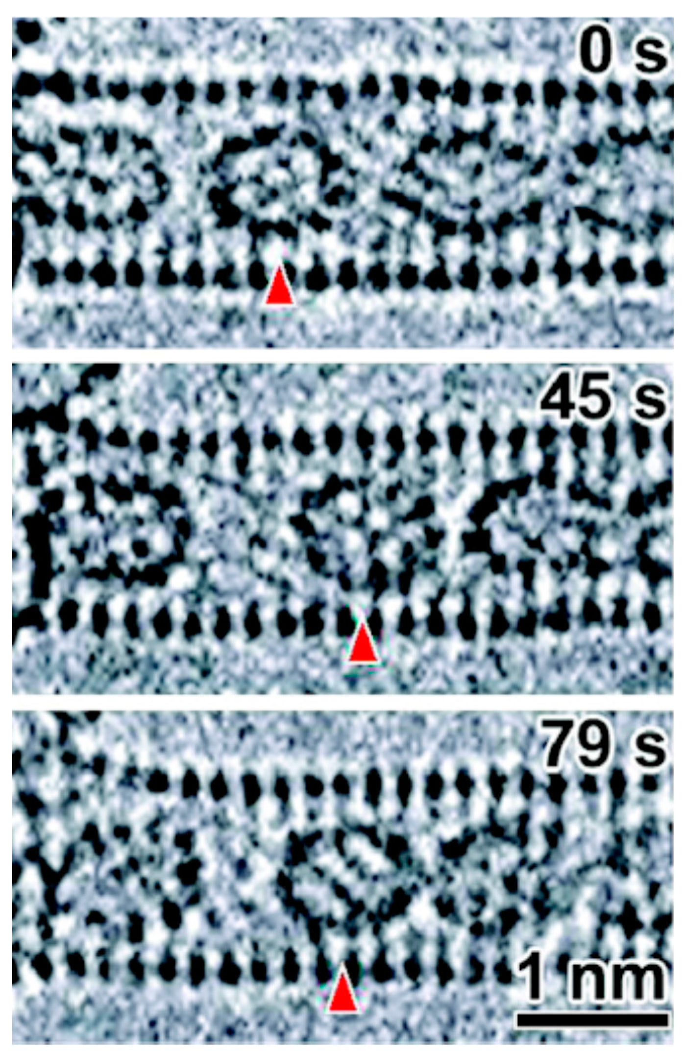
Figure 11.
Imaging and spectroscopy of a graphene edge, from work by Suenaga and Koshino. Reproduced with permission from [80]. Springer Nature, 2010. (a) Unprocessed ADF image of single graphene layer; Atomic positions are marked by circles in smoothed image (b). Scale bars, 0.5 nm. (d) ELNES of carbon K (1 s) spectra taken at the colour-coded atoms indicated in (b). Green, blue, and red spectra correspond to the normal sp2 carbon atom, a double-coordinated atom and a single-coordinated atom, respectively. These different states of atomic coordination are marked by coloured arrows in (a,b) and illustrated in (c).
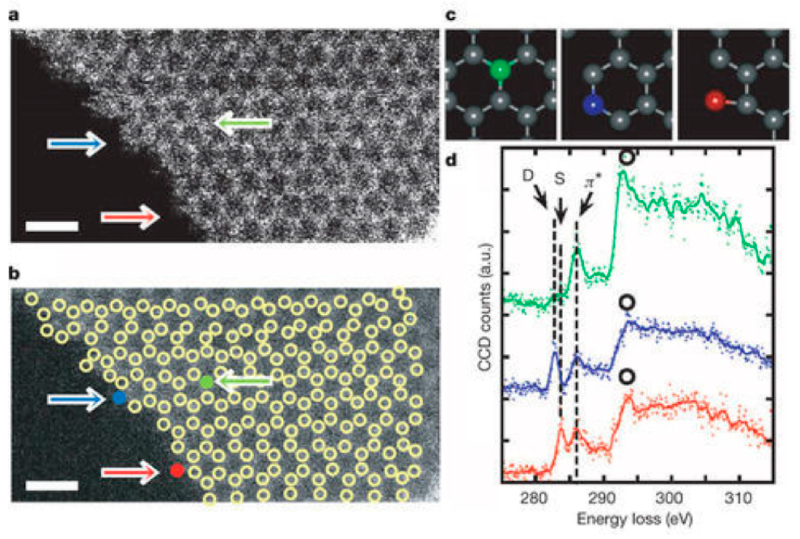
Figure 12.
(a) Exit wave function (EW) reconstruction TEM image of single and bilayer graphene sheets; (b,c) Higher magnification colourised images from parts of single and bilayer regions. Reproduced with permission from [94]. Elsevier, 2011.
Figure 12.
(a) Exit wave function (EW) reconstruction TEM image of single and bilayer graphene sheets; (b,c) Higher magnification colourised images from parts of single and bilayer regions. Reproduced with permission from [94]. Elsevier, 2011.

Figure 13.
Aberration corrected TEM image of diamond projected along <110>. (a) Magnified image. (b) Full image. An intensity profile is shown at upper right and a simulated image is shown as an insert in (a). From work by Hosokawa et al. Reproduced with permission from [98]. Oxford University Press, 2013.
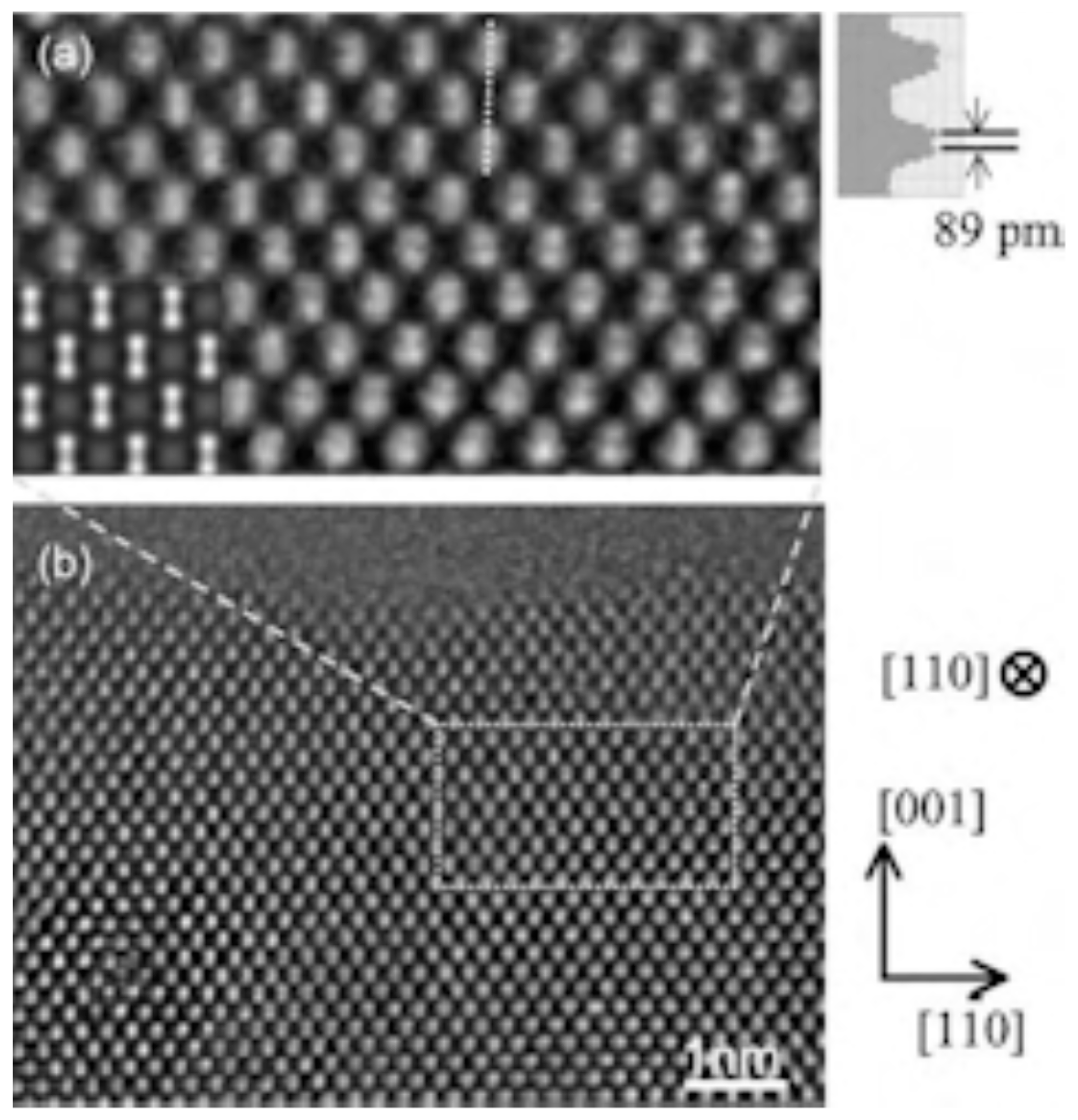
Figure 14.
Some of the pioneers of the study of carbon by TEM. Clockwise from top left: Trevor Evans, Robert Heidenreich, Kazu Suenaga, and Sumio Iijima.
Figure 14.
Some of the pioneers of the study of carbon by TEM. Clockwise from top left: Trevor Evans, Robert Heidenreich, Kazu Suenaga, and Sumio Iijima.
© 2018 by the author. Licensee MDPI, Basel, Switzerland. This article is an open access article distributed under the terms and conditions of the Creative Commons Attribution (CC BY) license (http://creativecommons.org/licenses/by/4.0/).
Share and Cite
MDPI and ACS Style
Harris, P.J.F. Transmission Electron Microscopy of Carbon: A Brief History. C 2018, 4, 4. https://doi.org/10.3390/c4010004
AMA Style
Harris PJF. Transmission Electron Microscopy of Carbon: A Brief History. C. 2018; 4(1):4. https://doi.org/10.3390/c4010004
Chicago/Turabian StyleHarris, Peter J. F. 2018. "Transmission Electron Microscopy of Carbon: A Brief History" C 4, no. 1: 4. https://doi.org/10.3390/c4010004
Note that from the first issue of 2016, this journal uses article numbers instead of page numbers. See further details here.