Morphological and Radio Frequency Characterization of Graphene Composite Films


1
Department of Information, Electronic and Telecom. Eng., ‘’La Sapienza’’ University, 00184 Roma, Italy
2
Department of Chemistry, Università di Genova, 16146 Genova, Italy
3
Department of Electronic and Telecom., Politecnico di Torino, 10128 Torino, Italy
*
Author to whom correspondence should be addressed.
C 2018, 4(2), 32; https://doi.org/10.3390/c4020032
Submission received: 16 April 2018
/
Revised: 15 May 2018
/
Accepted: 16 May 2018
/
Published: 20 May 2018
Abstract
:Graphene is a monolayer of carbon atoms which exhibits remarkable electronic and mechanical properties. Graphene based nano-materials have gained a lot of interest for many applications. In this paper, inks with three different graphene concentrations (12.5, 25, and 33 wt % in graphene) were prepared and deposited by screen printing. A detailed investigation of films’ surface morphology using Scanning Electron Microscope (SEM) and Atomic Force Microscopy (AFM) revealed that the graphene films present a homogeneous dispersion of the filler with a comparatively lower surface roughness at higher concentrations and negligible agglomerates. The films were then printed between copper electrodes on FR-4 substrate (trade name for glass-reinforced epoxy laminate material), commonly used in Radio Frequency (RF) circuits, and the measured scattering parameters analyzed. Finally, the reflection coefficient of a patch antenna, fabricated on FR-4 substrate with and without a stub loaded by a thin film were measured. The difference of the resonant frequency due to the different interaction between graphene flakes and polymer binders shows attractive features of functionalized graphene films for chemical and bio-sensing applications.
1. Introduction
Graphene is a two-dimensional (2D) structure with sp2 chemical bonds of carbon atoms, with remarkable electronic and mechanical properties amenable to several applications [1,2]. With proper solvent, surfactant and stabilizer chemistry, graphene flakes can be dispersed in different binders to produce inks with widely tunable rheology which can be used in conjunction with various printing methods [3]. There are several techniques to fabricate films, such as spin coating or drop casting [4], epitaxial growth [5], chemical vapor deposition [6], and, more recently, low cost deposition techniques such as screen printing [7], aerosol printing [8], transfer printing [9], and contact printing [10].
Graphene films have found many applications as electrochemical sensors (see e.g., [11]), biosensors [12], gas sensors (see e.g., [13,14]), humidity, temperature, and pressure monitoring [15]. Graphene electrical properties have been widely analyzed in the terahertz frequency [16] range where plasmonic effects occur. Recently, the practical utility of graphene in the microwaves frequency spectrum has been researched [17]. On the other hand, single-walled CNT (SWCNT) films have been already used for tuning microstrip patch antennas [18] demonstrating an 8% tunability range in the C-band frequency region. The frequency shift of CNT films has been found out to be beneficial for gas sensors in which the film’s dielectric, conductive or inductive properties have been modified upon exposure to gases (e.g., ammonia) [19]. The same principle has been exploited for biomedical applications such as breast cancer tumor cells detection [20] and glucose biosensor [21]. Also graphene-related structures (i.e., graphene oxide and reduced graphene oxide) have been successfully used as sensors [22] Nevertheless, investigations concerning the electrical properties of carbon nanostructured materials like graphene and carbon nanotubes in the microwave frequencies and their correlation to films’ morphological characteristics and composition are still scarce.
In this paper, the material effects of graphene films were investigated in the microwave frequencies. In particular, SEM (Scanning Electron Microscopy) and AFM (Atomic Force Microscopy) measurements and electrical characterization were used as a powerful set of tools to directly correlate the nature of the nano-fillers with the morphology of the nanocomposite films. Films with different concentrations (12.5%, 25%, and 33% in weight) were printed across the gap of a microstrip line and the results of a full-wave model compared with the measured scattering parameters. In addition, the best performing film (i.e., 33 wt %) was employed to tune the resonant frequency of a stub-loaded patch antenna.
2. Materials and Methods
Three α-terpineol (Sigma-Aldrich, Saint Louis, MO, USA, boiling point (b.p.) 220 °C) based screen printing pastes comprising a thermoplastic binder, additives, and different loads of graphene nanoplatelets, namely 12.5, 25, and 33 wt % were prepared. The first (i.e., 12.5 wt % of graphene) paste relied on an organic vehicle composed of 9.4 wt % of ethyl cellulose (EC) (Sigma-Aldrich, viscosity 0.01 Pa·s, 5% toluene/ethanol, 48% ethoxyl) and 78.1 wt % of α-terpineol. In this paste formulation, the ethyl cellulose acted as graphene nanoplatelets binder, thickener, and steric stabilizer. Nonetheless, the insulating character of this film (see results part) stemming from the low graphene load made the 12.5 wt % material unsuitable for RF resonator application. Thus, other two pastes containing a higher wt % of graphene were prepared. The original composition was modified by adding 7.5 wt % of castor oil (Sigma-Aldrich) for the case of the 25 wt % graphene load in order to plasticize the paste and compensate for the lower degree of printability due to the larger amount of carbon filler. A similar ethyl cellulose-based screen-printing pastes was prepared also for the 33 wt % graphene load. However, the filler dispersion, rheological behavior, and consequently the homogeneity and uniformity of the printed film were not optimal. Thus, a new composition comprised of 6.0 wt % of Butvar 98 polyvinyl-butyral (PVB, molecular weight 40,000−70,000 g/mol. determined by size exclusion chromatography, Sigma-Aldrich) and 1.7 wt % of polyvinyl-pyrrolidone (PVP, average molecular weight 360,000 g/mol., Sigma-Aldrich) and 3.1 wt % of linoleic acid (≥99%, Sigma-Aldrich) was prepared. The PVB and PVP polymers performed as binders. Furthermore, the latter was also used as a thickening agent in order to increase the paste viscosity and improve the thixotropic effect during the printing. It is worth noting that the lack of any cross-linking agent (i.e., transition metal salts) impeded the thermal curing of the linoleic acid. Therefore, the linoleic acid was employed only as wetting agent and dispersant additive to functionalize the graphene flakes surface and preventing their agglomeration. All the paste components had been pre-solubilized in anhydrous ethanol before being mixed and sonicated for 16 h by using a titanium ultrasonic horn. The ethanol was removed by rota-evaporation at 40 °C. The pastes containing the different graphene loads were printed in 3 × 3 mm2 the gap between a copper-etched microstrip onto an FR-4 substrate with a 230 mesh/inch polyester screen. Similarly, films were deposited at the end of a stub-loaded microstrip patch antenna etched on FR-4. A graphene film thickness of 10–20 µm was attained by multiple layers printing (i.e., one or two layers). A drying step between layers deposition was carried out at 125 °C. The final thermal curing aiming at evaporating the solvent (i.e., α-terpineol) was performed in a muffle (Thomas Scientific, Swedesboro, NJ, USA) at 160 °C.
Scanning electron microscopy micrographs of films were obtained by a Carl Zeiss Gemini 500 (Oberkochen, Baden-Württemberg, Germany) at an acceleration voltage of 5 keV. AFM (Asylum Research MFP-3D, 6310 Hollister Avenue, Santa Barbara, CA, USA) measurements at room temperature and air atmosphere were acquired by using an SPI 4000 system in the trapping mode. Data were analyzed through the Gwyddion software (Department of Nanometrology, Czech Metrology Institute, Brno, Czech Republic). Micro Raman data were collected with a Renishaw spectrometer (Wotton-under-Edge, Gloucestershire, UK) with excitation energy of 532 nm. A 50× objective was used for the characterization. The spectral resolution of the spectrometer was 2–3 cm−1 and laser power was kept well below 1 mW to avoid damage. The D, G, and 2D peaks were fitted with Lorentzian functions. Sheet resistance measurements on graphene films of one or two layers (each layer approximately 10 µm thick) screen-printed on FR-4 were performed by using the four-probe method with a Solatron 1286 electrochemical interface. Scattering parameters measurements with a Network Analyzer (E8361A, Keysight Agilent, Santa Rosa, CA, USA) were collected after standard open/short/load calibration.
3. Results
3.1. Morphology Characterization
3.1.1. Scanning Electron Microscope (SEM) and Atomic Force Microscopy (AFM)
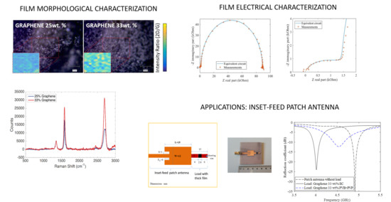
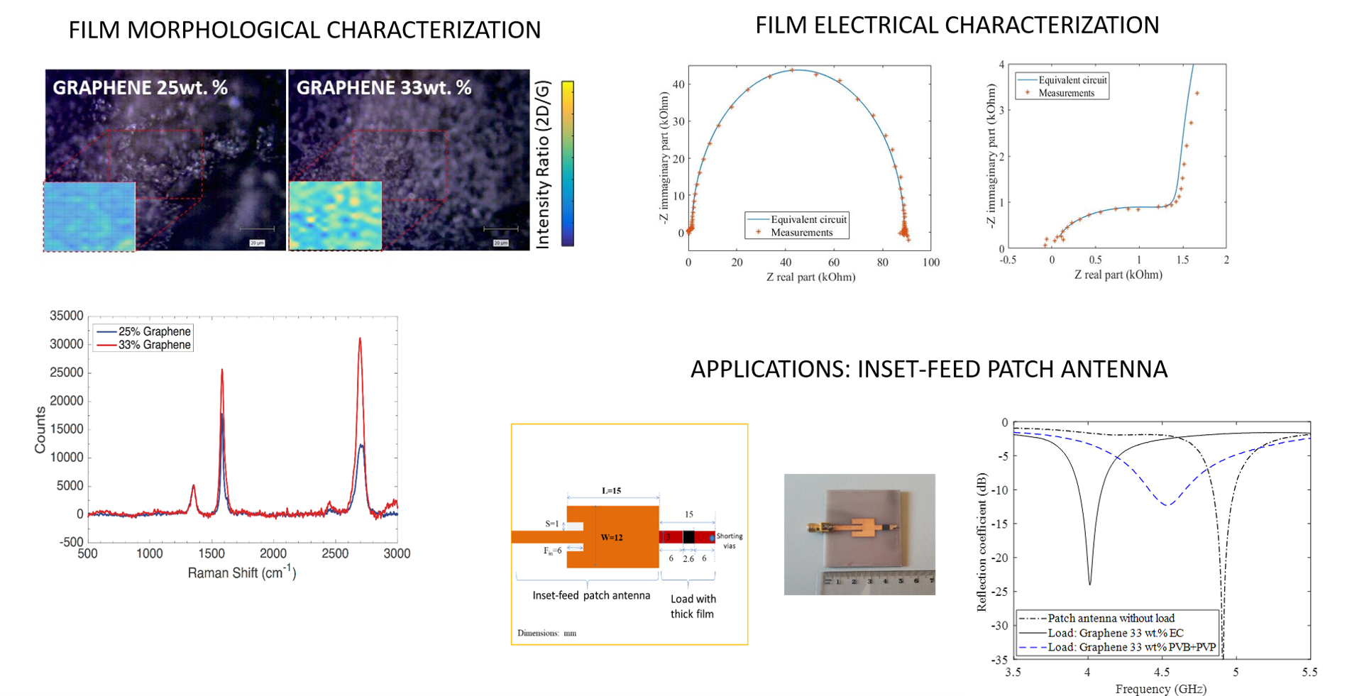
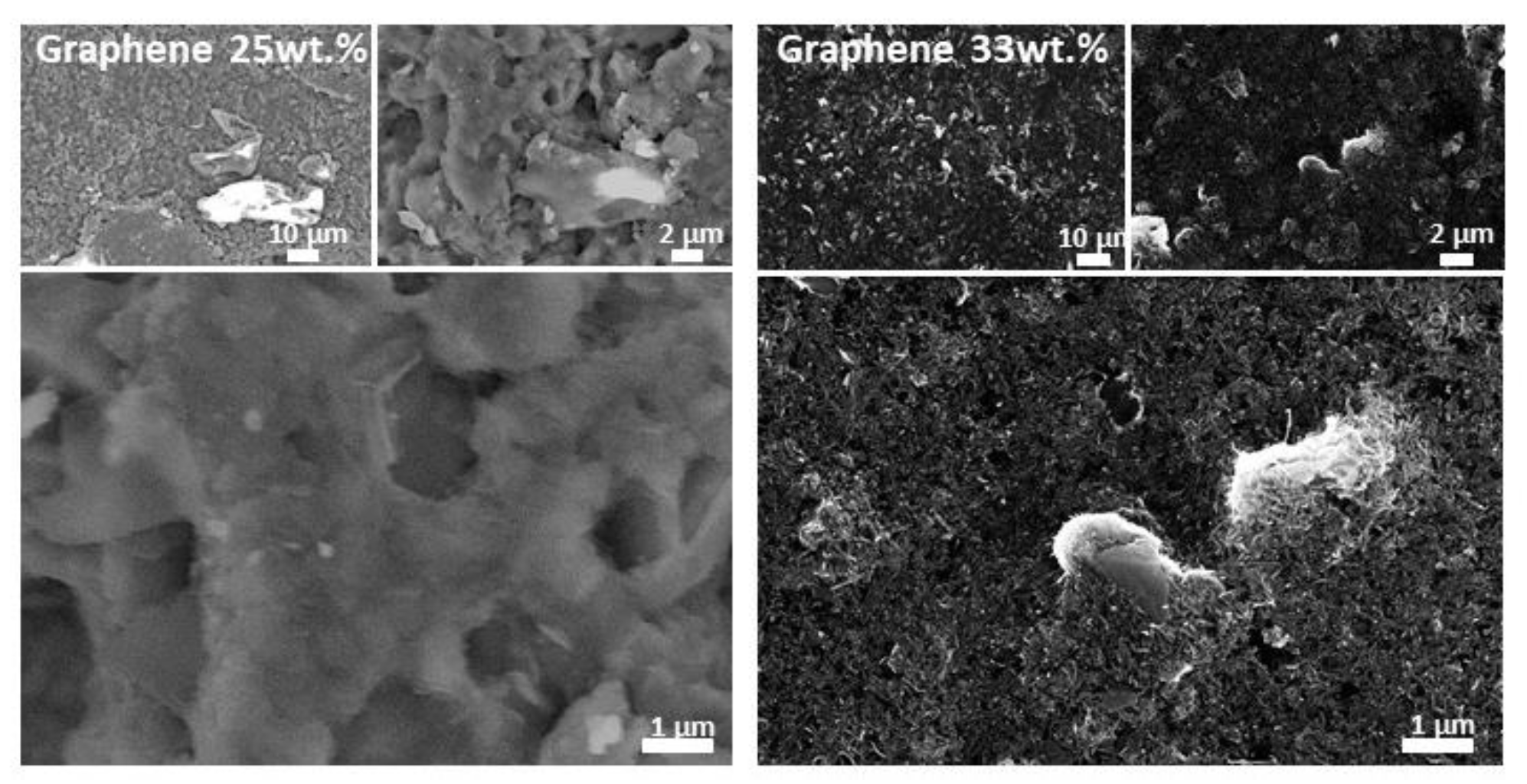
SEM, AFM, and electrical characterization, were used as a powerful set of tools to directly correlate the nature and concentration of the nano-fillers with the morphology of the nanocomposite films and their electrical and microwave properties. SEM micrographs of the 25 and 33 wt % are displayed in Figure 1. They indicate that in the 25 wt % (with ethyl cellulose) and in the 33 wt % film relying on the mixed PVB + PVP, graphene flakes were uniformly dispersed throughout the film. The graphene/polymer(s) structure were composed mainly of with lateral sizes flakes ranging from hundreds of nm to few micrometers. The analyzed polymers presented different topological features. The thickness of the clusters and lateral size of the grain distribution were obtained by data fitting using the lognormal distribution. AFM topological images together with their respective analyses are presented in Figure 2. While images could be collected for 33 wt % sample with the PVB + PVP binder, the 33 wt % composite with the ethyl cellulose could not be measured because of its high surface roughness. Indeed, 33 wt % films based on the ethyl-cellulose binder possesses a high level of rugosity and inhomogeneity compared to the same sample employing the PVB + PVP. Two reasons underlie such a behavior. First, the mixed binder is constituted by combination of non-polar (PVB) and polar (PVP) polymers possessing moderate (PVB) and high (PVP) molecular weight. Since both polarity and molecular weight affect profoundly the viscosity of polymer solutions and dispersion, the balance of the contraposing effects of the two binders may bring about the proper rheological behavior needed to print high concentrations of graphene. Hence, spreading of film on the substrate is greatly facilitated. Second, the presence of linoleic acid as a dispersant adds (through the absorption on the carbon filler) the stabilizing effect of the electrical repulsion stemming from the fat acid COO− groups to the steric repulsion given by the two binders [23]. Both effects (rheological and stabilizing) are reasonably missing in the 33 wt % film containing the sole ethyl cellulose. The relatively low roughness and homogeneity of the 25 wt % film (although rougher than the PVB + PVP one) can be ascribed to both the lower concentration of graphene and to the levelling effect, due to the castor oil [24].
3.1.2. Raman
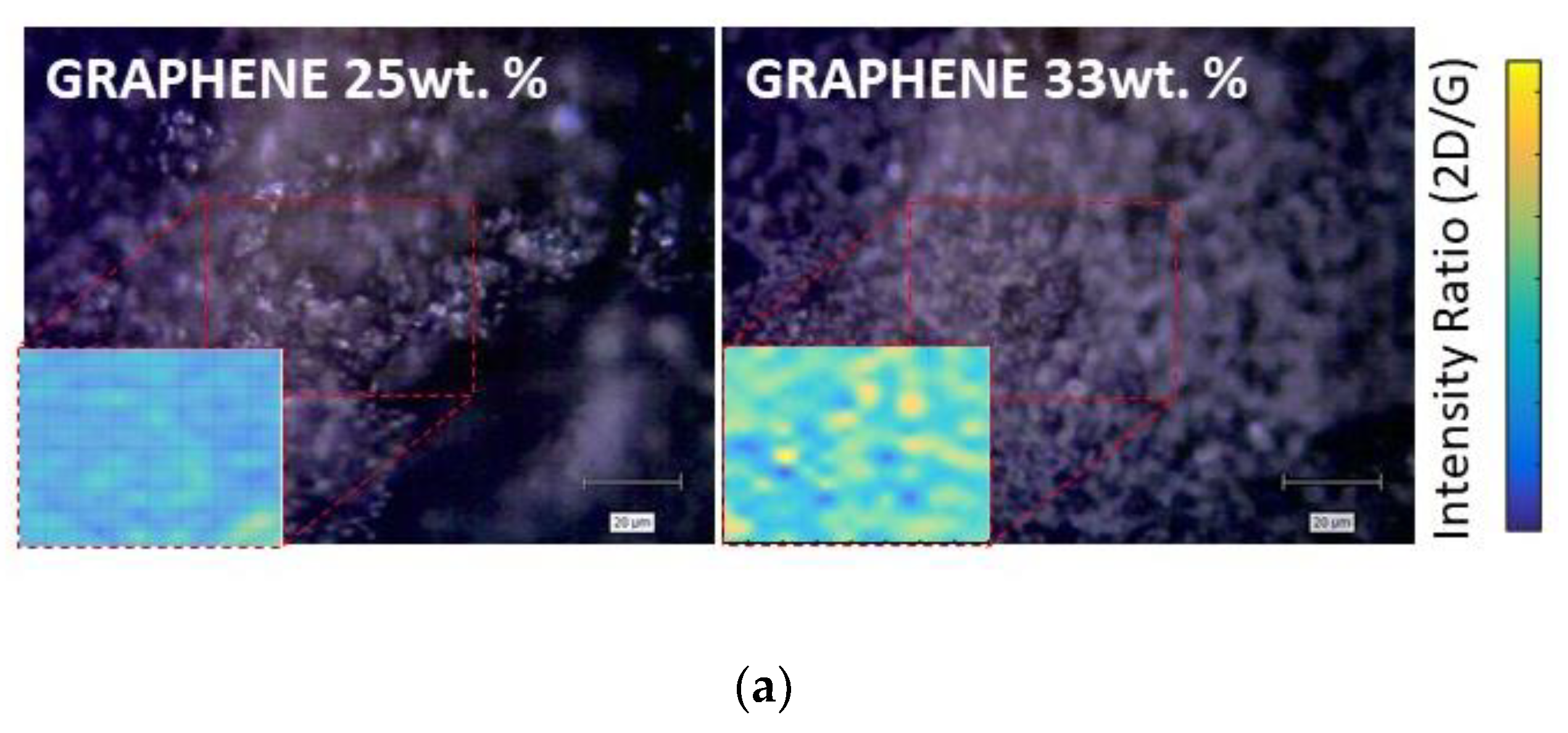
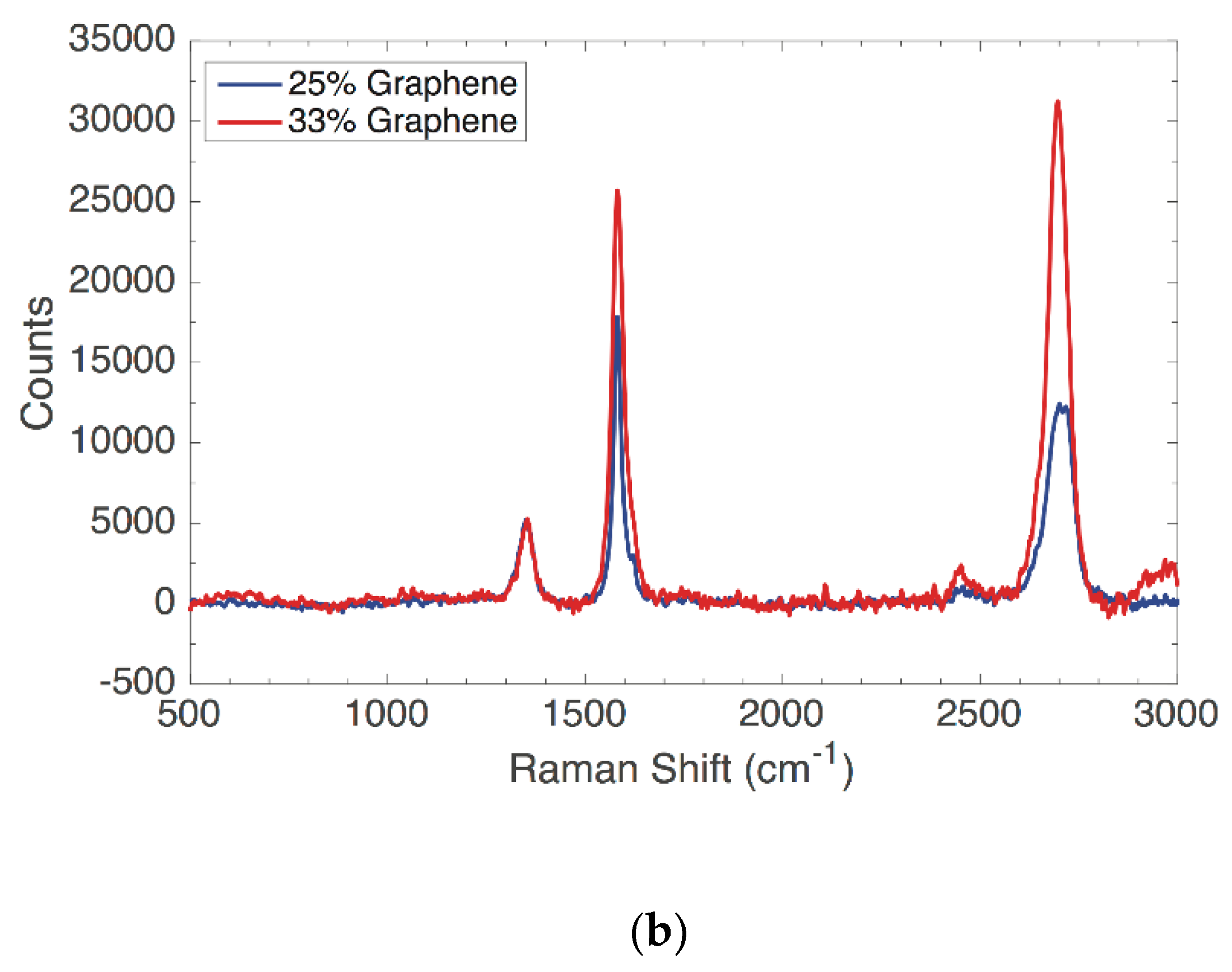
Raman measurements were carried out for each kind of nanocomposite by mapping a sample area of 100 × 100 μm2 and acquiring 100 spectra at a space interval of 10μm. Films with a concentration of 25% of graphene exhibited hyperspectral Raman maps with normally distributed graphite features. Most of the spectra presented a 2D/G ratio lower than one, as shown in Figure 3. Nevertheless, the 2D peak related to this distribution fitted with multiple Lorentians (2–4), suggesting the presence of a few graphite layers (mostly bi and three-layered) [25,26]. On the other side, it is worth noticing that films with a concentration of 33% of graphene showed as well normally distributed features owing to the graphene. The Raman spectra hyperspectral map showed a distribution predominantly characterized by flakes with a high 2D/G peak (>1.5) and a 2D peak that was possible to fit with one Lorentzian.
3.2. Electrical Characterization
The results obtained from the measurements of the sheet resistance on the films are summarized in Table 1. The two kinds of binders (ethyl cellulose and the PVB + PVP combination) and the 12.5 wt % are reported in the table along with the 25, and 33 wt % for sake of comparison. The sheet resistance (DC) decreased as the thickness of the film and the graphene concentration increased. The 12.5 wt % film had about the same order of resistance as the ethyl cellulose binder, indicating the insufficient interconnectivity of the graphene nanoplatelets at this concentration, whereas the 25 wt % possessed a sheet resistance in the order of hundreds of Ohms. This suggests that probably the percolation threshold of graphene nanoplatelets embedded into the ethyl cellulose matrix lies between 12.5 and 25 wt %. Not surprisingly, the 33 wt % films showed the lowest values of sheet resistance. The higher conductivity of films with 33 wt % or higher concentrations of graphene are of particular interest to RF applications where the line impedances can range from 25 to 200 Ω.
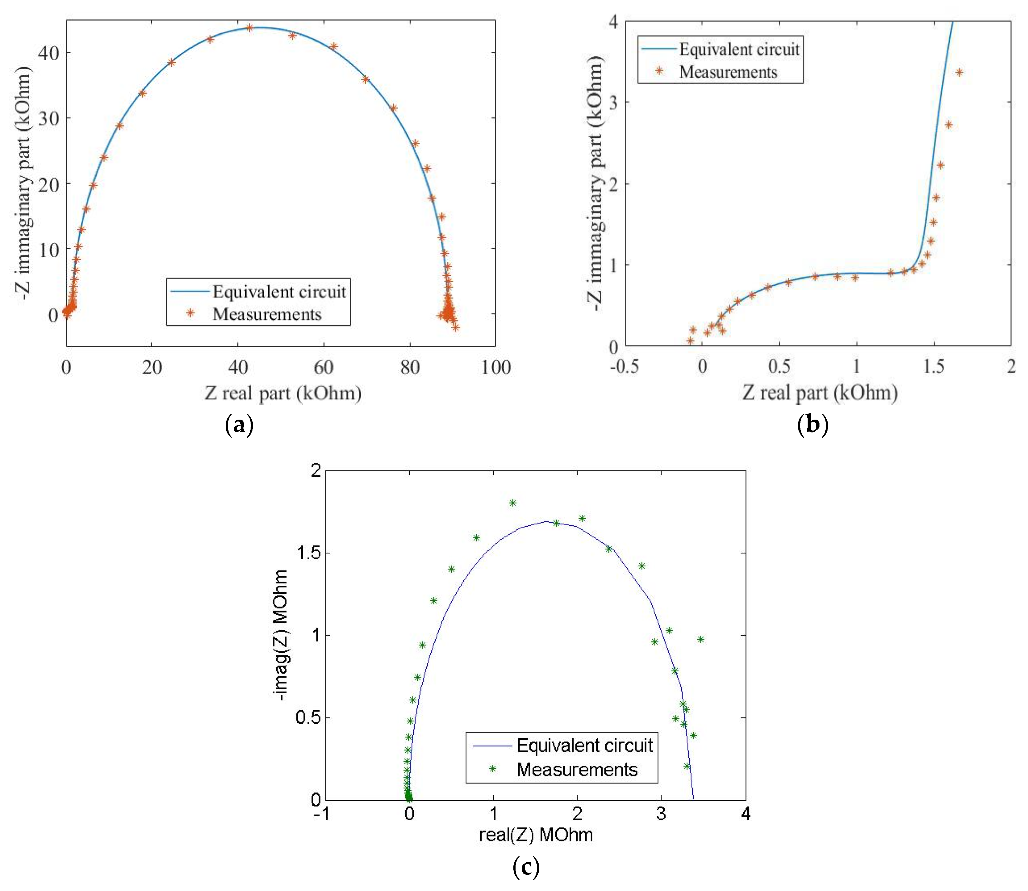
Data on dielectric spectroscopy between 0.1 Hz–32 MHz of the graphene film with 25 wt %, are shown in Figure 4 as Nyquist plots. The measured data were fitted with the frequency response of two series-connected parallel RC (Resistor-Capacitor) circuits, predicated on the dielectric response of a lossy insulators (ethyl cellulose) and the resistive-capacitive behavior of graphene flakes (due to graphene’s chemical capacitance and electron diffusion resistance) [27,28]. Figure 4b shows the detail of the high frequency region of Figure 5a where two parallel RC circuits representing the binder and the graphene contribution are evident. Graphene capacitance (i.e., the so called chemical capacitance due to the material’s density of state occupancy) extrapolated from a nonlinear fit of the impedance data is two orders of magnitude lower than the binder capacitance (7.06 pF for the graphene and 0.95 nF, for the ethyl cellulose). Similar values were found for the 33 wt % samples. Figure 4c reports, as an example, the Nyquist plot of the 12.5 wt % film. As expected, the sample can be modelled with a single RC accounting for the storage (i.e., real part of the dielectric constant) and dissipative component (i.e., the loss tangent) of the ethyl cellulose binder.
4. Discussion
4.1. Microstrip Lines Analysis
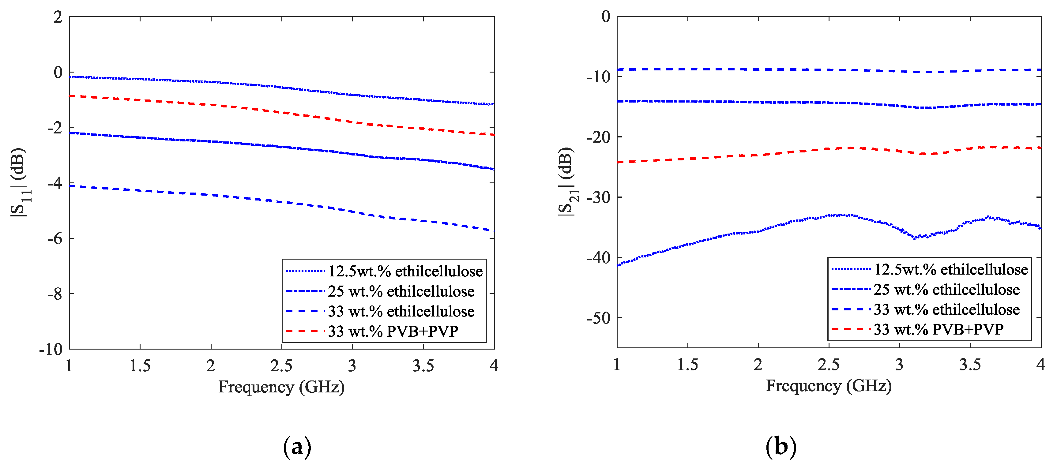
In order to understand the behavior of the films at the microwave frequencies, a micro strip line possessing a line width of 3 mm and gap spacing of 2.6 mm was photo-etched on a 1.56 mm thick FR-4 substrate (nominal dielectric constant of 4.3 and loss tangent of 0.03). By exploiting the deposition technique described in Section 2, a two-layer graphene film of 3 × 3 mm2 area was screen-printed within the gap. This configuration had been considered in [29] for two percentages of graphene (12.5 wt % and 25 wt %) and an ADS software (Advanced Design System, Keysight EEsof, Santa Rosa, CA, USA) model circuit had been proposed. The measured scattering parameters for the different graphene weight percentages are shown in Figure 5. A full wave analysis was performed with HFSS software (High Frequency Structure Simulator, Canonsburg, PA, USA). In the full-wave analysis, the film deposition is modelled as a surface impedance Z = (106 − j150) Ω for the case of graphene 12.5 wt %, Z = (450 − j120) Ω for the case of graphene 25 wt % and Z = (160 − j100) Ω for the 33 wt % case. As it was expected from the measurements of the sheet resistance and dielectric spectroscopy, the 12.5 wt % is practically indistinguishable from the binder matrix. The 33 wt % graphene films (with both the PVB + PVP binder and the ethyl cellulose) shows a marked increase in transmission across the gap due to reduced sheet resistance, while the 25 wt % film manifests an intermediate behavior.
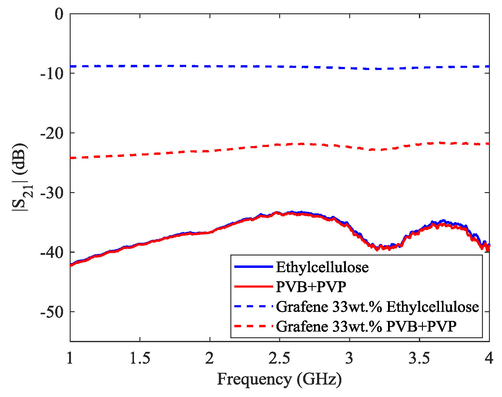
An interesting feature concerning the behavior of the two different binders with respect to the S21 parameter (transmission coefficient) can be noticed in Figure 6. Although the different nature of the two binders, their transmission coefficient curves show almost an identical trend throughout the explored frequency range.
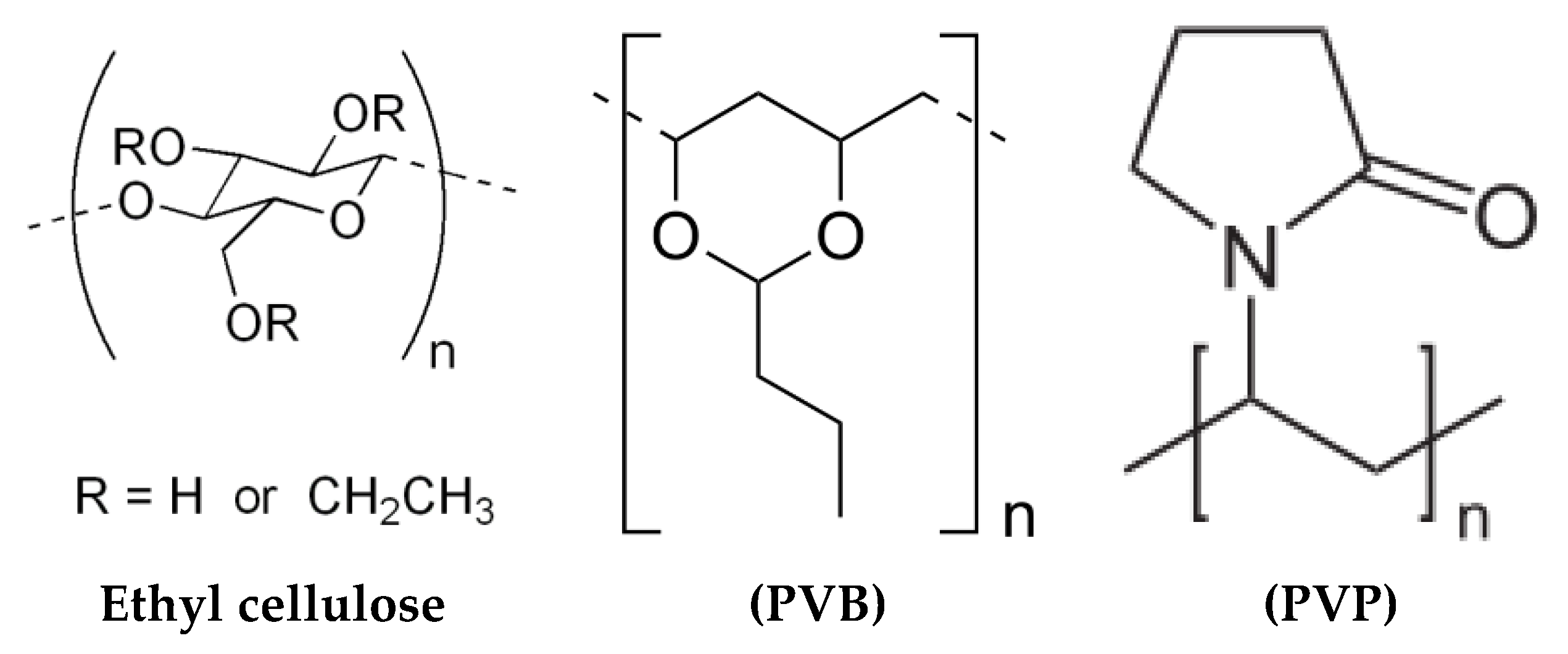
Probably, the transmission coefficient is dominated by the signal attenuation ascribable to the dielectric possessing the higher dielectric constant and loss tangent (i.e., the FR-4) [30,31]. Nevertheless, the chemical differences between the two binders can reflect into the different interaction (i.e., non-covalent) at the graphene Nano platelets/polymer interface [32,33]. Particularly, ethyl cellulose and PVB (Butvar 98) differ in the amount of OH groups as shown in Figure 7 (i.e., the level of ethoxylation in the ethyl cellulose, 48%, and the hydroxyl residues, 18–20% from the synthetic procedure of PVB, that is the condensation reaction between butyraldehyde and polyvinyl-alcohol Needless to say, such a difference affects the extension of the Hydrogen bonding in the two polymers, and consequently, the effect of Van der Waals interactions (e.g., dipole-dipole, dipole induced dipole, London dispersion forces, Hydrogen bonding) in the proximity of the graphene nano-platelets surface. Furthermore, the high polarity of the PVP component of the binder may also influence the dielectric characteristics of the graphene composite film. Besides, the linoleic acid adsorption (most likely through the covalent bonding of carboxylic groups on the filler’s surface) at the graphene/solvent interface in the screen printing paste modifies the surface electric properties (i.e., surface impedance) of the carbon filler [34,35]. Finally, the high surface roughness of the graphene-ethyl cellulose composite film compared to the graphene-PVB + PVP one could also impact on the surface impedance of the former. Hence, the combination of these different effect due to the two kinds of binders can reasonably account for the different transmission coefficient of the two 33 wt % graphene composite films.
4.2. Microstrip Patch Antenna
An inset-fed microstrip patch antenna was designed to operate at 4.8 GHz (patch 15 × 12 mm2, feed line width of 3 mm for 50 Ω impedance, see Figure 8 left panel). The feed inset and spacing (6 mm and 1 mm respectively) were chosen to provide the best impedance match between the feed line and the patch. The original design was modified by adding a stub of length of 15 mm, including a centered gap of 3 mm (load) as proposed in [36]. The antenna was fabricated on FR4 substrate (nominal dielectric constant of 4.3 and loss tangent of 0.02) (see Figure 8). An analysis on the effects of the position of the gap along the stub has been simulated in [37]. In such an analysis, the gap is centered and the measured return loss of different depositions has been investigated. In our case, 3 × 3 mm2 two layers thick graphene films (33 wt % EC or 33 wt % PVB + PVP binder) were deposited across the gap. As shown in Figure 8, the presence of the load formed by the stub and the film, considerably changes the response of the antenna. A large resonant frequency difference stemming from the two binders is observable. In fact, the introduction of the load comprising the 33 wt % graphene film employing the ethyl cellulose binder resonates at 4.1 GHz, whereas the load with the 33 wt % embedded in to the PVB + PVP binder resonates at 4.53 GHz. Once again, interactions between the graphene nano-platelets and the PVB + PVP binder could by one possible explanation. These interaction affects both the capacitance and the resistance of the film. As shown in [38] the resistance influence the return loss and the resonant frequency. In particular for the capacitance, it is suggested that a sufficient concentration (above the percolation threshold) of graphene nano-platelets entrapped into a polymer matrix can act as nanoscale capacitors modulating the gap dielectric constant. [38,39,40,41,42]. In other words, graphene nano-platelets act as the electrodes of a “classical” electrostatic nano-capacitor employing either the ethyl cellulose or the combined PVB + PVP binder (and FR-4 substrate) as dielectric. On the other hand, the microwave range of frequencies does not permit to detect any effect brought about by the graphene chemical capacitance [39,40]. Furthermore, the return loss shape at the resonance frequency is quite different for the two films. Indeed, the resonant peak due to the 33 wt % EC film is sharp, while the 33 wt % PVB + PVP peak appears broader. Such a feature is in agreement with the sheet resistance data presented in Table 1. Needless to say, further investigations must be conducted to gain a deeper insight concerning the graphene/binder interface and establish the nature of its effects on the radiofrequency properties of the composite films. Nevertheless, the present analysis suggests the possibility of changing the response of an antenna loaded with a stub in conjunction to a graphene thick films. Moreover the dependence of the resonant frequency on the film composition may allow for detection of biological relevant molecules, provided that the film’s surface is properly functionalized.
5. Conclusions
In this paper, the material parameters and electrical properties of graphene films in the microwave region of the electromagnetic spectrum were experimentally investigated. A detailed investigation of the surface morphology of the films using SEM and AFM revealed that the graphene filler was homogeneously dispersed over the film surface with a comparatively lower surface roughness at higher concentrations, and negligible agglomerates. A uniform distribution of the filler into the composite’s polymeric matrix can be achieved at high graphene (i.e., 33 wt %) concentrations by a proper combination of binders and dispersants (i.e., PVB, PVP, and linoleic acid). Sheet resistance measurement using the four-probe method on bare films compares reasonably well with the surface resistance derived from a full-wave analysis of films printed in between copper electrodes on FR-4 substrate. More specifically, an increasing trend in the conductivity with the number of printed layer and concentration of graphene was found. Furthermore, dielectric spectroscopy suggested a low-frequency (up to tens of MHz) behavior predicated on an insulating matrix (with storage and dissipative components) percolated by a conductive filler associated to a chemical (quantum) capacitance and to an electron transport resistance. Microstrip lines and patch antennas loaded with the graphene composites were fabricated to investigate the electrical properties of the films in the microwaves. Transmission (and reflection) coefficients of copper etched microstrips, turned out to depend not only on the graphene concentration but also on the binder composition. Also in the case of inset-feed patch antenna loaded by a given film, it has been observed that the resonance frequency of the antenna depends on the film composition.
Further studies to clarify the influence of ethyl cellulose, PVB, PVP different polarity, polarizability), and capability of creating hydrogen bonds on the surface impedance of graphene in the microwaves region are currently taking place. Moreover, the covalent adsorption of “small surfactants” (i.e., linoleic acid) on the graphene surface and its effect on RF electrical properties is also being investigated.
Author Contributions
S.Q. did the screen printing and the dc-measurements; M.M. did the morphological analysis; A.B. contributed to the lines and antenna realization and made the HFSS simulations; P.S. made the scattering parameters measurements, analyzed data and wrote the paper with S.Q.
Conflicts of Interest
The authors declare no conflict of interest.
References
- Geim, A.K.; Novoselov, K.S. The rise of grapheme. Nat. Mater. 2007, 6, 183–191. [Google Scholar] [CrossRef] [PubMed]
- Geim, A.K. Graphene: Status and prospects. Science 2009, 324, 1530–1534. [Google Scholar] [CrossRef] [PubMed]
- Li, B.; Zhong, W.-H. Review on polymer/graphite nanoplatelet nanocomposites. Mater. Sci. 2011, 46, 5595–5614. [Google Scholar] [CrossRef]
- Yoon Bae, S.; Jeon, I.; Yang, Y.; Park, N.; Suk Shin, H.; Park, S.; Ruoff, R.S.; Dai, L.; Beom Baek, J. Large-Area Graphene Films by Simple Solution Casting of Edge-Selectively Functionalized Graphite. ACS Nano 2011, 5, 4974–4980. [Google Scholar]
- Tetlow, H.; de Boer, P.J.; Ford, I.J.; Vvedensky, D.D.; Coraux, J.; Kantorovich, L. Growth of epitaxial graphene: Theory and experiment. Phys. Rep. 2014, 542, 195–295. [Google Scholar] [CrossRef]
- Zhang, Y.; Zhang, Y.; Zhou, C. Review of Chemical Vapor Deposition of Graphene and Related Applications. Acc. Chem. Res. 2013, 46, 2329–2339. [Google Scholar] [CrossRef] [PubMed]
- Cao, X.; Chen, H.; Gu, X.; Liu, B.; Wang, W.; Cao, Y.; Wu, F.; Zhou, C. Screen Printing as a Scalable and Low-Cost Approach for Rigid and Flexible Thin-Film Transistors Using Separated Carbon Nanotubes. ACS Nano 2014, 8, 12769–12776. [Google Scholar] [CrossRef] [PubMed]
- Jones, C.S.; Lu, X.; Renn, M.; Stroder, M.; Shih, W.-S. Aerosol-jet-printed, high-speed, flexible thin-film transistor made using single-walled carbon nanotube solution. Microelectron. Eng. 2010, 87, 434–437. [Google Scholar] [CrossRef]
- Zhou, Y.; Hu, L.; Grüner, G. A method of printing carbon nanotube thin films. Appl. Phys. Lett. 2006, 88, 109–123. [Google Scholar] [CrossRef]
- Liu, C.-X.; Choi, J.-W. Patterning conductive PDMS nanocomposite in an elastomer using microcontact printing. J. Micromech. Microeng. 2009, 19, 085019. [Google Scholar] [CrossRef]
- Cinti, S.; Arduini, F. Graphene-based screen-printed electrochemical (bio)sensors and their applications: Efforts and criticisms. Biosens. Bioelectron. 2017, 89, 107–122. [Google Scholar] [CrossRef] [PubMed]
- Hill, E.W.; Vijayaragahvan, A.; Novoselov, K. Graphene sensors. IEEE Sens. J. 2011, 11, 3161–3170. [Google Scholar] [CrossRef]
- Chou, J.-C.; Chen, J.-S.; Liao, Y.-H.; Lai, C.-H.; Yan, S.-J.; Huang, M.-S.; Wu, T.-Y. Fabrication and Characteristic Analysis for Enzymatic Glucose Biosensor Modified by Graphene Oxide and Magnetic Beads Based on Microfluidic Framework. IEEE Sens. J. 2017, 17, 1741–1748. [Google Scholar] [CrossRef]
- Su, W.; Xu, J.; Ding, X. An Electrochemical pH Sensor Based on the Amino-Functionalized Graphene and Polyaniline Composite Film. IEEE Trans. Nanobiosci. 2016, 15, 812–819. [Google Scholar] [CrossRef] [PubMed]
- Novikov, S.; Satrapinsky, A.; Lebedeva, N.; Iisakka, I. Sensitivity optimization of epitaxial graphene-based gas sensors. IEEE Trans. Instrum. Meas. 2013, 62, 1859–1864. [Google Scholar] [CrossRef]
- Leng, X.; Li, W.; Luo, D.; Wang, F. Differential Structure with Graphene Oxide for Both Humidity and Temperature Sensing. IEEE Sens. J. 2017, 17, 4357–4364. [Google Scholar] [CrossRef]
- Sanaeepour, M.; Abedi, A.; Sharifi, M.J. Performance Analysis of Nanoscale Single Layer Graphene Pressure Sensors. IEEE Trans. Electron Devices 2017, 64, 1292–1296. [Google Scholar] [CrossRef]
- Kymakis, E.; Stratakis, E.; Stylianakis, M.M.; Koudoumas, E.; Fotakis, C. Spin coated graphene films as the transparent electrode in organic photovoltaic devices. Thin Solid Films 2011, 520, 1238–1241. [Google Scholar] [CrossRef]
- Novikov, S.; Satrapinsky, A.; Lebedeva, N.; Iisakka, I. Fabrication and Study of Large Area QHE Devices Bases on Epitaxial Graphene. IEEE Trans. Instrum. Meas. 2015, 64, 1533–1538. [Google Scholar] [CrossRef]
- Bedzyk, M.J.; Arnold, M.S.; Hersam, M.C.; Guisinger, N.P. Electronic and mechanical properties of graphene-germanium interfaces grown by chemical vapor deposition. Nano Lett. 2015, 15, 7414–7420. [Google Scholar]
- Hyun, W.J.; Secor, E.B.; Hersam, M.C.; Frisbie, C.D.; Francis, L.F. High-Resolution Patterning of Graphene by Screen Printing with a Silicon Stencil for Highly Flexible Printed Electronics. Adv. Mater. 2015, 27, 109–115. [Google Scholar] [CrossRef] [PubMed]
- Hazra, S.K.; Basu, S. Graphene-Oxide Nano Composites for Chemical Sensor Applications. J. Carbon Res. 2016, 2, 12. [Google Scholar] [CrossRef]
- Mollet, H.; Grubenmann, A.; Payne, V. Formulation Technology: Emulsions, Suspensions, Solid Forms; Wiley: New York, NY, USA, 2008. [Google Scholar]
- Schönfeldt, N. Surface Active Ethylene Oxide Adducts; Elsevier: Amsterdam, The Netherlands, 1969. [Google Scholar]
- Bokobza, L.; Bruneel, J.-L.; Couzi, M. Raman Spectra of Carbon-Based Materials (from Graphite to Carbon Black) and of Some Silicone Composites. J. Carbon Res. 2015, 1, 77–94. [Google Scholar] [CrossRef]
- Peter, J.; Harris, F. Transmission Electron Microscopy of Carbon: A Brief History. J. Carbon Res. 2018, 4, 4. [Google Scholar] [CrossRef]
- Wang, Y.Y.; Pham, T.D.; Zand, J.K.; Li, P.; Burke, P.J. Charging the quantum capacitance of graphene with a single biological ion channel. ACS Nano 2014, 8, 428–438. [Google Scholar] [CrossRef] [PubMed]
- Zhan, C.; Neal, C.; Wu, J.; Jiang, D. Quantum effects on the capacitance of graphene-based electrodes. J. Chem. Phys. C 2015, 119, 22297–22303. [Google Scholar] [CrossRef]
- Torgvonikov, I.G. Dielectric Properties of Wood and Wood-Based Materials; Springer Series in Wood Science: Berlin, Germany, 1993. [Google Scholar]
- Coombs, C.F. Printed Circuits Handbook, 6th ed.; McGraw-Hill: New York, NY, USA, 2006. [Google Scholar]
- Zinenko, T.L.; Matsushima, A.; Nosich, A.I. Surface-plasmon, grating-mode and slab-mode resonances in THz wave scattering by a graphene strip grating embedded into a dielectric slab. IEEE J. Sel. Top. Quant. Electron. 2017, 23, 4601809. [Google Scholar] [CrossRef]
- Hassan, M.; Walter, M.; Moseler, M. Interactions of polymers with reduced graphene oxide: Van der Waals binding energies of benzene on graphene with defects. Phys. Chem. Chem. Phys. 2014, 16, 33–37. [Google Scholar] [CrossRef] [PubMed]
- Layek, R.K.; Nandi, A.K. A review on synthesis and properties of polymer functionalized graphene. Polymer 2013, 54, 5087–5103. [Google Scholar] [CrossRef]
- Xanthos, M. Functional Fillers for Plastics, 2nd ed.; Wiley: New York, NY, USA, 2010; pp. 112–119. [Google Scholar]
- Sowpati, A.K.; Nelo, M.; Palukuru, V.K.; Juuti, J.; Jantunen, H. Miniaturisation of dual band monopole antennas loaded with screen printed cobalt nanoparticle ink. IEEE Microw. Antennas Propag. 2013, 7, 180–186. [Google Scholar] [CrossRef]
- Naishadham, K. An investigation on the tunning of a microstrip patch antenna using carbon nanotube thin films. In Proceedings of the 2014 IEEE Antennas and Propagation Society International Symposium (APSURSI), Memphis, TN, USA, 6–11 July 2014. [Google Scholar] [CrossRef]
- Yasir, M.; Savi, P.; Bistarelli, S.; Cataldo, A.; Bozzi, M.; Pellegrini, L.; Bellucci, S. A Planar Antenna with Voltage-Controlled Frequency Tuning Based on Few-Layer Graphene. IEEE Antennas Wirel. Propag. Lett. 2017, 16, 2380–2383. [Google Scholar] [CrossRef]
- Savi, P.; Naishadham, K.; Bayat, A.; Giorcelli, M.; Quaranta, S. Multi-Walled Carbon Nanotube Thin Film Loading for Tuning Microstrip Patch Antennas. In Proceedings of the 10th European Conference on Antennas (EUCAP), Davos, Switzerland, 10–15 April 2016. [Google Scholar]
- Pierantoni, L.; Mencarelli, D.; Bozzi, M.; Moro, R.; Moscato, S.; Perregrini, L.; Micciulla, F.; Cataldo, A.; Bellucci, S. Broadband Microwave Attenuator Based on Few Layer Graphene Flakes. IEEE Trans. Microw. Theory Tech. 2015, 63, 2491–2497. [Google Scholar] [CrossRef]
- Bozzi, M.; Pierantoni, L.; Bellucci, S. Applications of Graphene at Microwave Frequencies. Radioengineering 2015, 24, 661–669. [Google Scholar] [CrossRef]
- Savi, P.; Naishadham, K.; Quaranta, S.; Giorcelli, M.; Bayat, A. Microwave Characterization of Graphene Films for Sensor Applications. In Proceedings of the IEEE International Instrumentation and Measurement Technology Conference (I2MTC), Torino, Italy, 22–25 May 2017; pp. 1–5. [Google Scholar]
- Xia, J.; Chen, F.; Li, J.; Tao, N. Graphene terahertz plasmon oscillators. IEEE Trans. Nanotechnol. 2008, 7, 91–99. [Google Scholar]
Figure 1.
Scanning electron microscopy (SEM) images: graphene 25 wt % ethyl cellulose and graphene 33 wt % Butvar 98 polyvinyl-butyral (PVB) + polyvinyl-pyrrolidone (PVP).
Figure 1.
Scanning electron microscopy (SEM) images: graphene 25 wt % ethyl cellulose and graphene 33 wt % Butvar 98 polyvinyl-butyral (PVB) + polyvinyl-pyrrolidone (PVP).

Figure 2.
Atomic force microscopy (AFM). Graphene 25 wt % ethyl cellulose and graphene 33 wt % PVB + PVP.
Figure 2.
Atomic force microscopy (AFM). Graphene 25 wt % ethyl cellulose and graphene 33 wt % PVB + PVP.

Figure 3.
Raman measurements on a sample area of 100 × 100 μm2 of graphene 25 wt % (ethyl cellulose) and graphene 33 wt % (PVB + PVP) (a); Raman peaks intensity (b).
Figure 3.
Raman measurements on a sample area of 100 × 100 μm2 of graphene 25 wt % (ethyl cellulose) and graphene 33 wt % (PVB + PVP) (a); Raman peaks intensity (b).


Figure 4.
Nyquist Plot of graphene 25 wt %. (a) full frequency range, (b) high-frequencies zoom, (c) Nyquist Plot of graphene 12.5 wt %.
Figure 4.
Nyquist Plot of graphene 25 wt %. (a) full frequency range, (b) high-frequencies zoom, (c) Nyquist Plot of graphene 12.5 wt %.

Figure 5.
Measurements of the scattering parameters of the various films deposition: (a) magnitude of the reflection coefficient S11, (b) magnitude of the transmission coefficient S21.
Figure 5.
Measurements of the scattering parameters of the various films deposition: (a) magnitude of the reflection coefficient S11, (b) magnitude of the transmission coefficient S21.

Figure 6.
Measured S21 parameter for the ethyl cellulose and PVB + PVP binders, and the respective films loaded with 33 wt % of graphene.
Figure 6.
Measured S21 parameter for the ethyl cellulose and PVB + PVP binders, and the respective films loaded with 33 wt % of graphene.

Figure 7.
Chemical structure of the binders contained in the graphene films (33 wt %) ethyl cellulose, PVB and PVP.
Figure 7.
Chemical structure of the binders contained in the graphene films (33 wt %) ethyl cellulose, PVB and PVP.

Figure 8.
Patch antenna with a graphene film (a,b). Measured reflection coefficient for different load conditions (stub + graphene film 33 wt % EC and stub+ graphene film 33 wt % PVP + PVB) (c).
Figure 8.
Patch antenna with a graphene film (a,b). Measured reflection coefficient for different load conditions (stub + graphene film 33 wt % EC and stub+ graphene film 33 wt % PVP + PVB) (c).


Table 1.
DC sheet resistance (Ω/square).
| Sample | One-Layer | Two-Layer |
|---|---|---|
| Ethyl cellulose (EC) | >2 × 10⁸ | >2 × 10⁸ |
| PVB + PVP | >2 × 10⁸ | >2 × 10⁸ |
| 12.5 wt % EC | >2 × 10⁸ | >2 × 10⁸ |
| 25.0 wt % EC | 650 | 440 |
| 33.0 wt % EC | 280 | 110 |
| 33.0 wt % PVB + PVP | 240 | 160 |
© 2018 by the authors. Licensee MDPI, Basel, Switzerland. This article is an open access article distributed under the terms and conditions of the Creative Commons Attribution (CC BY) license (http://creativecommons.org/licenses/by/4.0/).
Share and Cite
MDPI and ACS Style
Quaranta, S.; Miscuglio, M.; Bayat, A.; Savi, P. Morphological and Radio Frequency Characterization of Graphene Composite Films. C 2018, 4, 32. https://doi.org/10.3390/c4020032
AMA Style
Quaranta S, Miscuglio M, Bayat A, Savi P. Morphological and Radio Frequency Characterization of Graphene Composite Films. C. 2018; 4(2):32. https://doi.org/10.3390/c4020032
Chicago/Turabian StyleQuaranta, Simone, Mario Miscuglio, Ahmad Bayat, and Patrizia Savi. 2018. "Morphological and Radio Frequency Characterization of Graphene Composite Films" C 4, no. 2: 32. https://doi.org/10.3390/c4020032
Note that from the first issue of 2016, this journal uses article numbers instead of page numbers. See further details here.