Article

Silicene Nanoribbons on Pb-Reconstructed Si(111) Surface †

by
Agnieszka Stȩpniak-Dybala
*,
Mieczysław Jałochowski
and
Mariusz Krawiec
Institute of Physics, M. Curie-Sklodowska University, Pl. M. Curie-Skłodowskiej 1, 20-031 Lublin, Poland
*
Author to whom correspondence should be addressed.
Part of this work has been presented at the International Conference on Atomically Controlled Surfaces Interfaces and Nanostructures (ACSIN2016), Frascati, Rome, Italy, 9–15 October 2016.
Condens. Matter 2016, 1(1), 8; https://doi.org/10.3390/condmat1010008
Submission received: 10 November 2016 / Revised: 27 November 2016 / Accepted: 29 November 2016 / Published: 5 December 2016

Abstract

:
We report on the initial stage of growing of silicon nanostructures on Pb-induced 3 × 3 and 3 × 7 reconstructed Si(111) surfaces. The deposition of 0.75 monolayer of Si at a temperature of around 200 K results in Si nanoribbons a few-nanometers in length running in three equivalent high symmetry directions of Si(111) surface, as revealed by low temperature scanning tunneling microscopy measurements. The nanoribbons are predominantly 1.6 nm wide and show local 3 × 3 reconstruction. These findings are interpreted within the framework of silicene nanoribbons grown on a bare Si(111) surface.

1. Introduction

The discovery of graphene and the observation of its remarkable properties [1] have boosted an intensive search for similar materials with a two-dimensional (2D) honeycomb geometry, mainly composed of group-IV elements [2,3,4]. Among them, silicene—a silicon counterpart of graphene—has attracted increasing attention, owing to its promise of being easily integrated with the present Si-based electronics [5,6,7,8,9]. Indeed, the first silicene-based field effect transistor operating at room temperature was recently demonstrated [10].
The planarity of a single layer of Si atoms, named as silicene [11], was predicted theoretically in 1994 by Takeda and Shiraishi [12], and its dynamical stability has been confirmed [13]. In contrast to graphene, silicene is not completely planar, and features a low buckled geometry with two vertically displaced sublattices. The physical origin of the buckling comes from the orbital hybridization of silicon, with sp 3 being preferred. In spite of this geometry, the outstanding electronic properties, characteristic of graphene, are also preserved in silicene. Moreover, silicene has several advantages over graphene. It has stronger spin–orbit coupling, which may lead to detectable non-trivial topological phases [14,15,16,17,18], and it can easily be functionalized [19,20,21,22,23,24,25].
Despite the theoretical predictions, the synthesis of silicene continues to be a significant challenge. So far silicene has been successfully grown on only a few substrates, either as a 2D layer on Ag(111), ZrB 2 , Ir(111), Al(111), ZrC(111), and MoS 2 [26,27,28,29,30,31,32,33,34], or in the form of nanoribbons on Ag(110) and Au(110) [35,36,37,38,39,40]. Beyond monolayer silicene, multilayer silicene films and nanoribbons have also been grown on Ag substrates [41,42,43,44].
However, the substrate usually introduces substantial modifications to structural and electronic properties of silicene, altering its free-standing characteristics. Indeed, in the case of Ag, two different bond angles between Si atoms can be identified, characteristic of sp 2 and sp 3 hybridization. As a result, an almost-flat silicene layer with Si atoms sticking out is observed. Such a peculiar arrangement of atoms is a consequence of the electronic mechanism protecting the Dirac spectrum from degradation, as was theoretically discovered [18,25]. However, there are firm arguments for strong hybridization between the silicene and the Ag substrate states. The protecting mechanism fails, since the interaction is very strong—it is too strong to maintain the linear electronic spectrum or even the 2D character of the silicene layer [45,46,47]. On the other hand, if the silicene–substrate interaction is weak, it might be impossible to grow silicene, due to the preferred sp 3 bonding of Si atoms, and their tendency for clustering.
Searching for substrates on which to grow silicene is an important issue. Though silicene has only been grown on very few surfaces, a number of candidates have been theoretically predicted and proposed as potentially suitable for silicene formation [25,48,49,50,51]. Recently, lead was proposed as a potential candidate to grow silicene [51]. The calculated binding energy of silicene to a Pb(111) surface is three times lower than for silicene on Ag(111), and an order of magnitude higher than in the case of silicene on a typical weakly-interacting substrate. As a result, the Dirac spectrum is only slightly modified, with the main contribution of the 3p z orbitals of Si atoms.
Here, we report on the first attempt to grow silicene nanostructures on a substrate containing Pb atoms. We have chosen 3 × 3 and 3 × 7 reconstructions of Pb—in short, 3 -Pb and 7 -Pb—on a Si(111) surface. The deposition of a 0.75 monolayer of Si at a temperature of around 200 K, followed by annealing, results in Si nanoribbons a few-nanometers in length running in three equivalent high-symmetry directions of the Si(111) surface, as revealed by low temperature scanning tunneling microscopy and spectroscopy (STM and STS) measurements. The nanoribbons are predominantly 1.6 nm wide and show local 3 × 3 reconstruction. These findings are interpreted within the framework of silicene nanoribbons on a bare Si(111) surface. The deposited Si atoms directly bind to the surface Si atoms, expelling Pb atoms, and form pure Si nanoribbons. This scenario is corroborated by first-principles density functional theory (DFT) calculations. Pb atoms play an important role in this process, as they stabilize the Si(111) surface and control the growth of silicene nanoribbons. These findings open new routes for the creation of silicene nanostructures on silicon surfaces.

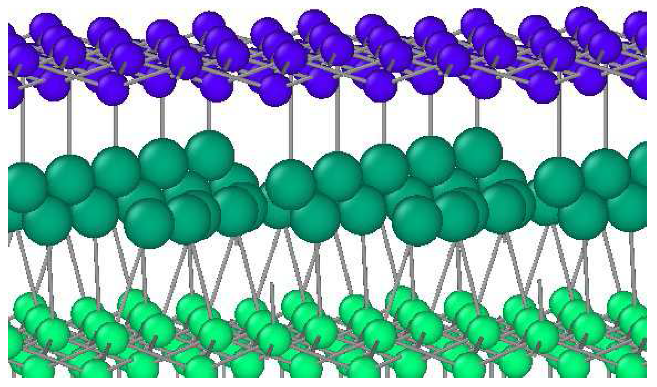
2. Materials and Methods

All experiments were performed under ultrahigh vacuum (UHV) conditions with a 4 He-cooled scanning tunneling microscope (Omicron, Taunusstein, Germany) working at 4.5 K. An n-type Si(111) single crystal with a resistivity of 1–5 m Ω · cm was used as the substrate crystal. A clean Si(111) surface was obtained by flashing the sample to 1420 K under UHV conditions. Then, the sample was annealed at 1140 K for a few minutes and slowly cooled down to room temperature (RT). This procedure leads to the formation of a spatially extended well-ordered Si(111)7×7 phase [52]. The Pb was evaporated from a crucible on the Si(111)7×7 surface held at RT. Subsequently, a little more than a monolayer of Pb was first evaporated at RT, followed by a post-annealing at 560 K for 1 min. This led to the desorption of Pb in excess of the first layer [53], and a Pb wetting layer with patches of 3 -Pb and 7 -Pb structure was obtained [54]. In order to get extended 7 -Pb structure, the sample was annealed at 560 K for 3 min. Next, the Si layer was evaporated by direct current heating of a pure silicon chip on to the sample held at 200 K within 20 min. We have performed the deposition of around 0.75 monolayer (ML). To obtain the presented Si structures, the sample was first annealed at room temperature for 1 h, and next, by direct current heating, at around 400 K for 5 min. The amount of the evaporants (Pb and Si) was measured during deposition by quartz crystal balance monitor.
The STM and STS measurements were done with electrochemically-etched W tips. The tunneling conductance spectra ( d I / d V ) were acquired using a lock-in technique with a root mean square modulation amplitude of 12 mV at frequency 3.3 kHz.
Density functional theory calculations were performed within Perdew–Burke–Ernzerhof (PBE) [55] generalized gradient approximation (GGA) using projector-augmented-wave potentials, as implemented in VASP (Vienna ab-initio simulation package) [56,57]. The plane wave energy cutoff for all calculations was set to 340 eV, and the Brillouin zone was sampled by a 5 × 5 × 1 Monkhorst–Pack k-points grid [58]. The spin–orbit interaction was omitted.
The Si(111)–Pb system has been modeled by eight Si double layers and the reconstruction layer. A vacuum region of 20 Å was added to avoid the interaction between surfaces of the slab. All of the atomic positions were relaxed, except the bottom layer, until the largest force in any direction was below 0.01 eV/Å. The Si atoms in the bottom layer were fixed at their ideal bulk positions and saturated with hydrogen. The lattice constant of Si was fixed at the calculated value, 5.47 Å.

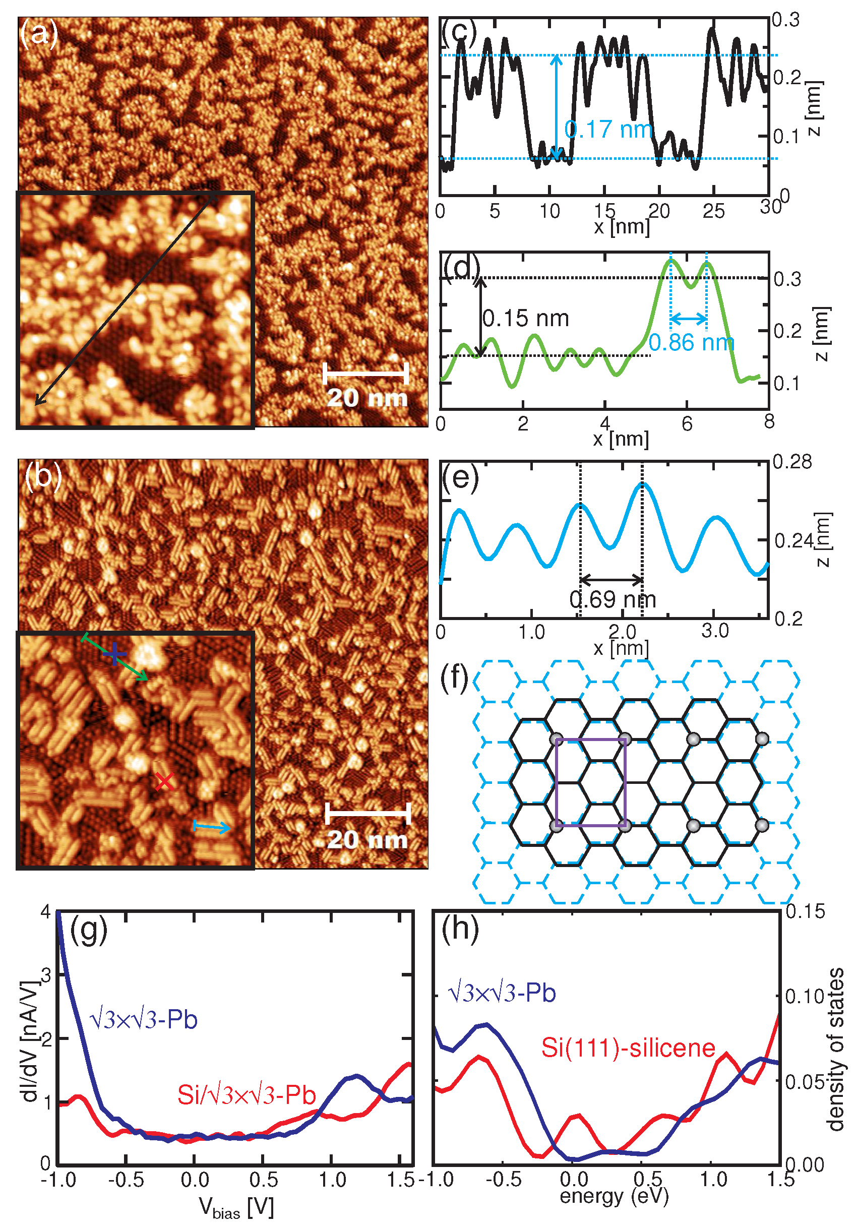
3. Results and Discussion

Figure 1a shows an STM topography image of Si(111) 3 × 3 -Pb surface. Typical 3 -Pb patches—known as a dense Pb phase (10.44 Pb atoms/nm 2 )—separated by domain walls are observed.
The domain walls are composed of a striped Pb phase—a less dense phase (9.40 Pb atoms/nm 2 ) with 7 -Pb reconstruction—which appears darker in the constant current STM image [59,60]. The STM topography of the striped Pb phase is shown in Figure 1b [61]. The one-dimensional character of the reconstruction is clearly visible. Corresponding STS characteristics are shown in Figure 1c,d. The resonances observed at U = 1.3 V in panel (c) and at U = 2.0 V in (d) are the signatures of the 3 -Pb and 7 -Pb phases, respectively [62].
The inset of Figure 1a is a close view STM of the single layer Pb/Si(111). Bright spots in the STM image are resolved here as triangular structures. The 3 -Pb structure features four Pb atoms for every three Si atoms—i.e., a coverage of 4/3 ML. Another one-atomic-layer film of Pb (presented in Figure 1b) has a smaller coverage of 6/5 ML. In a unit cell of the 7 -Pb phase, there are six Pb atoms per five surface Si atoms. These reconstructions were used as templates to grow Si nanostructures.
Before presenting the results of our experiments, it is instructive to learn about theoretical predictions regarding silicene on a Pb-decorated Si(111) surface. Figure 2 shows the calculated structural model of silicene on a Si(111) 3 × 3 -Pb surface.
At first sight, it seems that after relaxation of atomic positions, the silicene layer retains its free-standing buckled form. It features a hexagonal honeycomb lattice with neighboring Si atoms displaced alternatively perpendicular to the surface, forming two sublattices. Indeed, this structure differs from silicene on a typical metallic substrate, where the arrangement of atoms features two different characteristic angles, as discussed in Section 1. In the present case, all the angles are approximately equal to 112 , which suggests a mixed sp 2 /sp 3 hybridization of silicene electron states with stronger sp 3 contribution than in the freestanding case. The impact of the substrate on the atomic structure of silicene is only to increase the buckling by 0.21 Å from its freestanding value of 0.45 Å. The mean silicene–substrate separation yields 3.27 Å. These structural findings are reflected in quite low binding energy of silicene to the substrate ( E b ). The binding energy is the energy gain per Si atom after the deposition of the silicene on the Si(111) 3 × 3 -Pb surface, and in the present case, it yields 140 meV. The value of E b is around three times lower than in the case of the silicene on Ag(111) [63], and comparable to the silicene on a hydrogenated Si(111) surface [46]. It is worth noting that the binding energy of silicene on Si(111) 3 × 3 -Pb is only slightly lower than in the case of Pb(111) surface [25,51]. In view of completely different atomic structures of silicene on both substrates, this is somehow a surprising result, and can be explained in terms of the passivation of Si(111) surface bonds by Pb atoms, similar as for a hydrogenated surface [46].
Since the binding energy of silicene to 3 -Pb is rather low, it is natural to ask about the growing possibility. Calculated cohesive energy ( E c )—the energy gain to from silicene on the 3 -Pb from isolated Si atoms—is lower than the cohesive energy of Si in diamond structure by 0.49 eV, and only slightly higher than for free-standing silicene. Note that in the case of the Ag(111) surface, where silicene was successfully grown, the E c is close to the cohesive energy of Si in diamond structure. Thus, growing silicene may be challenging due to the tendency of Si atoms for clustering. Another problem is related to the high mobility of Pb atoms on Si surfaces, even at room temperature [64,65,66]. Therefore, experimental attempts to grow silicene on Pb-induced Si(111) reconstructions should be done at low temperatures.
To tackle the problem of silicene growth in the presence of Pb, we deposited 0.75 ML of Si on 3 -Pb reconstruction at various temperatures. The deposition of Si at temperatures higher than 215 K always resulted in rather small in diameter and 3.13 Å high atomic islands. Comparing STM and STS characteristics of the islands with corresponding characteristics recorded on 3 -Pb, we concluded that the islands are covered by Pb atoms. During the deposition process, Si atoms bond directly to the surface Si atoms, and expel Pb atoms from their original positions. This scenario is supported by the high mobility of Pb atoms on Si surfaces, and it naturally explains the height of the islands, which is close to the distance between (111) planes in bulk Si. Note that diffusion processes for Pb atoms on Si surfaces start to play a significant role at temperatures higher than 200 K [65].
At lower temperatures ( T < 200 K), Si atoms self-assemble into irregular islands of different shapes and heights. Of course, this behavior is a manifestation of the tendency of silicon toward clustering. In this case, Si adatoms also bond directly to the Si surface, expelling Pb atoms. However, since the Pb atoms are now less mobile, they are not expected to be on top of the Si islands. Although we cannot unambiguously confirm this scenario for 3 -Pb, we can deduce this conclusion from the adsorption of Si on the 7 -Pb surface, since Si islands grow only in the domain regions (i.e., between patches of the 3 -Pb reconstruction). Annealing the sample results in the same structures as obtained previously during the deposition of Si at higher temperatures (i.e., with Pb atoms on-top of the Si islands).
To shed additional light on the growth of Si nanostructures on Pb-induced surface reconstructions, we investigated 7 -Pb as a substrate. Basically, the situation is very similar to the case of the 3 -Pb; at high temperature ( T > 215 K), Pb-covered Si islands are observed, while at low temperature ( T < 200 K), irregular Si nanostructures appear. However, we can now prove Pb-free Si islands grown at low temperature. Namely, after the deposition of Si, the original 7 -Pb phase evolved into the 3 -Pb phase in areas between Si islands. Recalling the fact that the 7 -Pb phase is less dense than the 3 -Pb, this suggests that, expelled from Si islands, Pb atoms accommodate in the surface between the islands, forming the 3 -Pb phase. The 3 -Pb phase is clearly visible in Figure 3a, where the STM topography of the 7 -Pb covered by Si atoms deposited at T = 200 K is shown.
The Si nanostructures formed at T = 200 K are irregular and feature different diameters and heights (Figure 1b). The temperature is too low to induce more regular Si structures and possibly to cover them by Pb. Surprisingly, when we left the sample for one hour at room temperature, the originally disordered structures evolved into new phase with very short nanoribbons. Further annealing at T = 400 K for 5 min led to very regular nanoribbons, as Figure 3b demonstrates. The nanoribbons are a few nanometers long and 1.6 nm wide. As is evident, they run in three equivalent high-symmetry directions of the Si(111) surface. At first sight, the nanoribbons look like pairs of two Si chains separated by 0.86 nm (Figure 3d). However, as shown below, these structures are wide nanoribbons, not just separated chains. Note that similar (albeit shorter) nanoribbons also form on the 3 -Pb, but only in the domain regions, where the 7 -Pb phase originally developed.
The observed nanostructures are unlikely to be separated Si chains, for at least three reasons. First, the separation between chains is expected to be commensurate with some Si–Si distance on the Si(111) surface. However, it is difficult to assign any Si–Si distance to the measured value of 0.86 nm (Figure 3d). Second, the modulation of STM topography across and along these nanostructures is very similar, ∼ 0.4 0.5 Å—compare Figure 3d,e. Third, it is difficult to justify why the chains always grow in pairs. Therefore, we suggest that the observed structures are single nanoribbons. Moreover, they are silicene nanoribbons grown on a bare Si(111) surface. Such interpretation is supported by following facts. First of all, the observed 3 periodicity along the nanoribbons is characteristic for Si growth on a Si(111) surface [67,68], as well as for multilayer silicene [44]. The 3 × 3 -Si reconstruction features a single Si atom within the unit cell sticking out of the layer, with other Si atoms forming almost a flat structure. This is a consequence of sp 3 bonding, similar to the previously discussed silicene on Ag or Pb surfaces. Furthermore, the apparent height of nanoribbons measured with respect to the neighboring 3 -Pb phase, 0.15 nm, is reproduced well by present DFT calculations, 0.1 nm. Note that the theoretical value has been obtained only from geometrical considerations, neglecting the electronic contribution to the apparent height, always present in STM measurements [69]. The next point concerns the electronic properties as measured by STS (Figure 3g). The d I / d V characteristics acquired on top of nanoribbons substantially differ from the data collected on the 3 -Pb surface, as one can notice comparing, for example, positions of resonances. This is also an additional argument against Pb-composed nanoribbons. Importantly, the STS characteristics are qualitatively reproduced well by the calculated density of states of the 3 -Pb surface and silicene deposited on the bare Si(111) surface, shown in Figure 3h. Thus, in view of the above discussion, the observed nanostructures can be regarded as silicene nanoribbons grown on the bare Si(111) surface.
Now, a question appears about the internal structure of the nanoribbons. We can deduce a tentative structural model considering all the facts known from the STM measurements. First of all, the 3 periodicity along a nanoribbon can be easily achieved assuming its armchair edges with sticking-out Si atoms. Then, four Si hexagons fit well with the width of a nanoribbon. The proposed model is shown in Figure 3f. The model consists of silicene on a Si(111) surface with a slide-AA stacking, known from multilayer silicene [70]. This stacking features a honeycomb lattice shifted in one armchair direction with respect to the underneath layer. In the present case the, the silicene lattice has been divided into two parts and shifted in both directions other than nanoribbon edges. This results in deformed hexagons in the middle of the nanoribbon, as Figure 3f illustrates. This operation is required in order to match a width of the nanoribbon as well as distance between protrusions (sticking out Si atoms) observed in the STM experiment. Thus, the present model accounts for all the experimental findings regarding the nanoribbon structure.
Although the nanoribbons are composed of only Si atoms, it seems that Pb atoms play an important role in the present case. They stabilize the Si(111) surface, but also control the growth of silicene nanoribbons. Further analysis is required to understand the role of Pb atoms and to determine details and the energetic stability of the proposed model, which has been postponed for future DFT investigations.

4. Conclusions

In conclusion, we have studied the formation of silicene nanoribbons on a Pb-induced Si(111) surface. The deposition of 0.75 ML of Si at temperature around 200 K followed by annealing results in 1.6 nm wide and a few-nanometers long silicene nanoribbons running in three equivalent Si(111) high-symmetry directions. The nanoribbons feature local 3 ordering, and are interpreted in the framework of silicene nanoribbons grown on a bare Si(111) surface. A structural model has been proposed, and is related to the slide-AA stacking, known for silicene multilayers. These findings open new routes to creating silicene nanostructures on silicon surfaces.

Acknowledgments

The work has been supported by the National Science Centre (Poland) under Grant No. DEC- 2014/15/B/ST5/04244. Part of this work has been presented at the International Conference on Atomically Controlled Surfaces Interfaces and Nanostructures (ACSIN2016), Frascati, Rome, Italy, 9–15 October 2016 [71].

Author Contributions

A.S.-D. performed the STM/STS experiments; M.J. analyzed the data; M.K. performed the DFT calculations and wrote the paper.

Conflicts of Interest

The authors declare no conflict of interest.

References

  1. Novoselov, K.S.; Geim, A.K.; Morozov, S.V.; Jiang, D.; Katsnelson, M.I.; Grigorieva, I.V.; Dubonos, S.V.; Firsov, A.A. Two-dimensional gas of massless Dirac fermions in graphen. Nature 2005, 438, 197–200. [Google Scholar] [CrossRef] [PubMed] [Green Version]
  2. Bhimanapati, G.R.; Lin, Z.; Meunier, V.; Jung, Y.; Cha, J.; Das, S.; Xiao, D.; Son, Y.; Strano, M.S.; Cooper, V.R.; et al. Recent advances in two-dimensional materials beyond graphene. ACS Nano 2015, 12, 11509–11539. [Google Scholar] [CrossRef] [PubMed]
  3. Novoselov, K.S.; Mishchenko, A.; Carvalho, A.; Castro Neto, A.H. 2D materials and van der Waals heterostructures. Science 2016, 353. [Google Scholar] [CrossRef] [PubMed]
  4. Molle, A. Xenes: A new emerging two-dimensional materials platform for nanoelectronics. ECSP Trans. 2016, 75, 163–173. [Google Scholar] [CrossRef]
  5. Houssa, M.; Dimoulas, A.; Molle, A. Silicene: A review of recent experimental and theoretical investigations. J. Phys. Condens. Matter 2015, 27, 253002. [Google Scholar] [CrossRef] [PubMed]
  6. Le Lay, G.; Salomon, E.; Angot, T. Silicene: Silicon conquers the 2D world. Europhys. News 2016, 47, 17–21. [Google Scholar] [CrossRef]
  7. Grazanetti, C.; Cinquanta, E.; Molle, A. Two-dimensional silicon: The advent of silicene. 2D Mater. 2016, 3, 012001. [Google Scholar] [CrossRef]
  8. Zhao, J.; Liu, H.; Yu, Z.; Quhe, R.; Zhou, S.; Wang, Y.; Liu, C.C.; Zhong, H.; Han, N.; Lu, J.; et al. Rise of silicene: A competitive 2D material. Prog. Mater. Sci. 2016, 83, 24–151. [Google Scholar] [CrossRef]
  9. Molle, A.; Grazianetti, C.; Cinquanta, E. Silicene: Silicon at the two dimensional limit and its aplications to nanoelectronics. ECSP Trans. 2016, 75, 703–709. [Google Scholar] [CrossRef]
  10. Tao, L.; Cinquanta, E.; Chiappe, D.; Grazianetti, C.; Fanciulli, M.; Dubey, M.; Molle, A.; Akinwande, D. Silicene field-effect transistors operating at room temperature. Nat. Nanotechnol. 2015, 10, 227–231. [Google Scholar] [CrossRef] [PubMed]
  11. Guzmán-Verri, G.G.; Lew Yan Voon, L.C. Electronic structure of silicon-based nanostructures. Phys. Rev. B 2007, 76, 075131. [Google Scholar] [CrossRef]
  12. Takeda, K.; Shiraishi, K. Theoretical possibility of stage corrugation in Si and Ge analogs of graphite. Phys. Rev. B 1994, 50, 14916. [Google Scholar] [CrossRef]
  13. Cahangirov, S.; Topsakal, M.; Aktürk, E.; Sahin, H.; Ciraci, S. Two- and One-Dimensional Honeycomb Structures of Silicon and Germanium. Phys. Rev. Lett. 2009, 102, 236804. [Google Scholar] [CrossRef] [PubMed]
  14. Liu, C.C.; Feng, W.; Yao, Y. Quantum spin Hall effect in silicene and two-dimensional germanium. Phys. Rev. Lett. 2011, 107, 076802. [Google Scholar] [CrossRef] [PubMed]
  15. Tahir, M.; Manchon, A.; Sabeeh, K.; Schwingenschlögl, U. Quantum spin/valley Hall effect and topological insulator phase transitions in silicene. Appl. Phys. Lett. 2013, 102, 162412. [Google Scholar] [CrossRef]
  16. Wu, S.C.; Shan, G.; Yan, B. Prediction of Near-Room-Temperature Quantum Anomalous Hall Effect on Honeycomb Materials. Phys. Rev. Lett. 2014, 113, 256401. [Google Scholar] [CrossRef] [PubMed]
  17. Zhang, X.L.; Liu, L.F.; Liu, W.M. Quantum anomalous Hall effect and tunable topological states in 3d transition metals doped silicene. Sci. Rep. 2013, 3, 2908. [Google Scholar] [CrossRef] [PubMed]
  18. Podsiadły-Paszkowska, A.; Krawiec, M. Spin-polarized gapped Dirac spectrum of unsupported silicene. Appl. Surf. Sci. 2016, 373, 45–50. [Google Scholar] [CrossRef]
  19. Drummond, N.D.; Zolyomi, V.; Falko, V.I. Electrically tunable band gap in silicene. Phys. Rev. B 2012, 85, 075423. [Google Scholar] [CrossRef]
  20. Ni, Z.; Liu, Q.; Tang, K.; Zheng, J.; Zhou, J.; Qin, R.; Gao, Z.; Yu, D.; Lu, J. Tunable Bandgap in Silicene and Germanene. Nano Lett. 2012, 12, 113–118. [Google Scholar] [CrossRef] [PubMed]
  21. Yan, J.A.; Gao, S.P.; Stein, R.; Coard, G. Tuning the electronic structure of silicene and germanene by biaxial strain and electric field. Phys. Rev. B 2015, 91, 245403. [Google Scholar] [CrossRef]
  22. Gürel, H.H.; Özcelik, V.O.; Ciraci, S. Effects of charging and perpendicular electric field on the properties of silicene and germanene. J. Phys. Condens. Matter 2013, 25, 305007. [Google Scholar] [CrossRef] [PubMed]
  23. Van den Broek, B.; Houssa, M.; Scalisea, E.; Pourtoisb, G.; Afanas‘ev, V.V.; Stesmans, A. First-principles electronic functionalization of silicene and germanene by adatom chemisorption. Appl. Surf. Sci. 2014, 291, 104–108. [Google Scholar] [CrossRef]
  24. Podsiadły-Paszkowska, A.; Krawiec, M. Electrical and mechanical controlling of the kinetic and magnetic properties of hydrogen atoms on free-standing silicene. J. Phys. Condens. Matter 2016, 28, 284004. [Google Scholar] [CrossRef] [PubMed]
  25. Podsiadły-Paszkowska, A.; Krawiec, M. Silicene on metallic quantum wells: an efficient way of tuning silicene-substrate interaction. Phys. Rev. B 2015, 92, 165411. [Google Scholar] [CrossRef]
  26. Vogt, P.; De Padova, P.; Quaresima, C.; Avila, J.; Frantzeskakis, E.; Asensio, M.C.; Resta, A.; Ealet, B.; Le Lay, G. Silicene: Compelling experimental evidence for graphenelike two-dimensional silicon. Phys. Rev. Lett. 2012, 108, 155501. [Google Scholar] [CrossRef] [PubMed]
  27. Feng, B.; Ding, Z.; Meng, S.; Yao, Y.; He, X.; Cheng, P.; Chen, L.; Wu, K. Evidence of Silicene in Honeycomb Structures of Silicon on Ag(111). Nano Lett. 2012, 12, 3507–3511. [Google Scholar] [CrossRef] [PubMed]
  28. Lin, C.L.; Arafune, R.; Kawahara, K.; Tsukahara, N.; Minamitani, E.; Kim, Y.; Takagi, N.; Kawai, M. Structure of silicene grown on Ag(111). Appl. Phys. Express 2012, 5, 045802. [Google Scholar] [CrossRef]
  29. Jamgotchian, H.; Colington, Y.; Hamazaouri, N.; Ealet, B.; Hoarau, J.; Aufray, B.; Biberian, J.P. Growth of silicene layers on Ag(111): Unexpected effect of the substrate temperature. J. Phys. Condens. Matter 2012, 24, 172001. [Google Scholar] [CrossRef] [PubMed]
  30. Fleurence, A.; Friedlein, R.; Ozaki, T.; Kawai, H.; Wang, Y.; Yamada-Takamura, Y. Experimental evidence for epitaxial silicene on diboride thin films. Phys. Rev. Lett. 2012, 108, 245501. [Google Scholar] [CrossRef] [PubMed]
  31. Meng, L.; Wang, Y.; Zhang, L.; Du, S.; Wu, R.; Li, L.; Zhang, Y.; Li, G.; Zhou, H.; Hofer, W.A.; et al. Buckled silicene formation on Ir(111). Nano Lett. 2013, 13, 685–690. [Google Scholar] [CrossRef] [PubMed]
  32. Morishita, T.; Spencer, M.J.S.; Kawamoto, S.; Snook, I.K. A new surface and structure for silicene: Polygonal silicene formation on the Al(111) surface. J. Phys. Chem. C 2013, 117, 22142. [Google Scholar] [CrossRef]
  33. Aizawa, T.; Suehara, S.; Otani, S. Silicene on Zirconium Carbide (111). J. Phys. Chem. C 2014, 118, 23049. [Google Scholar] [CrossRef]
  34. Chiappe, D.; Scalise, E.; Cinquanta, E.; Granzietti, C.; van der Broek, B.; Fanciulli, M.; Houssa, M.; Molle, A. Two-dimensional Si nanosheets with local hexagonal structure on a MoS2 surface. Adv. Mater. 2014, 26, 2096–2101. [Google Scholar] [CrossRef] [PubMed]
  35. Sahaf, H.; Masson, L.; Leandri, C.; Aufray, B.; Le Lay, G. Formation of a one-dimensional grating at the molecular scale by self-assembly of straight silicon nanowires. Appl. Phys. Lett. 2007, 90, 263110. [Google Scholar] [CrossRef]
  36. Kara, A.; Leandri, C.; Davila, M.E.; De Padova, P.; Ealet, B.; Oughaddou, H.; Aufray, B.; Le Lay, G. Physics of silicene stripes. J. Supercond. Nov. Magn. 2009, 22, 259–263. [Google Scholar] [CrossRef]
  37. De Padova, P.; Quaresima, C.; Ottaviani, C.; Sheverdyaeva, P.M.; Moras, P.; Carbone, C.; Topwal, D.; Olivieri, B.; Kara, A.; Oughaddou, H.; et al. Evidence of graphene-like electronic signature in silicene nanoribbons. Appl. Phys. Lett. 2010, 96, 261905. [Google Scholar] [CrossRef]
  38. De Padova, P.; Quaresima, C.; Olivieri, B.; Perfetti, P.; Le Lay, G. sp2-like hybridization of silicon valence orbitals in silicene nanoribbons. Nano Lett. 2011, 98, 081909. [Google Scholar]
  39. Feng, B.; Li, H.; Meng, S.; Chen, L.; Wu, K. Structure and quantum well states in silicene nanoribbons on Ag(110). Surf. Sci. 2016, 645, 74–79. [Google Scholar] [CrossRef]
  40. Tchalala, M.R.; Enriquez, H.; Mayne, A.J.; Kara, A.; Roth, S.; Silly, M.G.; Bendounan, A.; Sirotti, F.; Greber, T.; Aufray, B.; et al. Formation of one-dimensional self-assembled silicon nanoribbons on Au(110)-(2×1). Appl. Phys. Lett. 2013, 102, 083107. [Google Scholar] [CrossRef]
  41. Leandri, C.; Le Lay, G.; Aufray, B.; Girardeaux, C.; Avila, J.; Dávila, M.E.; Asensio, M.C.; Ottaviani, C.; Cricenti, A. Self-aligned silicon quantum wires on Ag(110). Surf. Sci. 2005, 574, L9–L15. [Google Scholar] [CrossRef]
  42. De Padova, P.; Vogt, P.; Resta, A.; Avila, J.; Razado-Colambo, I.; Quaresima, C.; Ottaviani, C.; Olivieri, B.; Bruhn, T.; Hirahara, T.; et al. Evidence of Dirac fermions in multilayer silicene. Appl. Phys. Lett. 2013, 102, 163106. [Google Scholar] [CrossRef]
  43. De Padova, P.; Avila, J.; Resta, A.; Razado-Colambo, I.; Quaresima, C.; Ottaviani, C.; Olivieri, B.; Bruhn, T.; Vogt, P.; Asensio, M.C.; et al. The quasiparticle band dispersion in epitaxial multilayer silicene. Appl. Phys. Lett. 2013, 102, 163106. [Google Scholar] [CrossRef]
  44. De Padova, P.; Generosi, A.; Paci, B.; Ottaviani, C.; Quaresima, C.; Olivieri, B.; Salomon, E.; Angot, T.; Le Lay, G. Multilayer silicene: Clear evidence. 2D Mater. 2016, 3, 031011. [Google Scholar] [CrossRef]
  45. Wang, Y.; Cheng, H. Absence of a Dirac cone in silicene on Ag(111): First-principles density functional calculations with a modified effective band structure technique. Phys. Rev. B 2013, 87, 245430. [Google Scholar] [CrossRef]
  46. Guo, Z.; Furuya, S.; Iwata, J.I.; Oshiyama, A. Absence and presence of Dirac electrons in silicene on substrates. Phys. Rev. B 2013, 87, 235435. [Google Scholar] [CrossRef]
  47. Lin, C.; Arafune, R.; Kawahara, K.; Kanno, M.; Tsukahara, N.; Minamitani, E.; Kim, Y.; Kawai, M.; Takagi, N. Substrate-induced symmetry breaking in silicene. Phys. Rev. Lett. 2013, 110, 076801. [Google Scholar] [CrossRef] [PubMed]
  48. Liu, H.; Gao, J.; Zhao, J. Silicene on Substrates: A Way To Preserve or Tune Its Electronic Properties. J. Phys. Chem. C 2013, 117, 10353–10359. [Google Scholar] [CrossRef]
  49. Kanno, M.; Arafune, R.; Lin, C.L.; Minamitani, E.; Kawai, M.; Takagi, N. Electronic decoupling by h-BN layer between silicene and Cu(111): A DFT-based analysis. New J. Phys. 2014, 16, 105019. [Google Scholar] [CrossRef]
  50. Zhu, J.; Schwingenschlögl, U. Structural and Electronic Properties of Silicene on MgX2 (X = Cl, Br, and I). Appl. Mater. Interfaces 2014, 6, 11675–11681. [Google Scholar] [CrossRef] [PubMed]
  51. Podsiadły-Paszkowska, A.; Krawiec, M. Dirac fermions in silicene on Pb(111) surface. Phys. Chem. Chem. Phys. 2015, 17, 2246–2251. [Google Scholar] [CrossRef] [PubMed]
  52. Schwartzentruber, B.S.; Mo, Y.W.; Webb, M.B.; Legally, M.G. Scanning tunneling microscopy studies of structural disorder and steps on Si surfaces. J. Vac. Sci. Technol. A 1989, 7, 2901. [Google Scholar] [CrossRef]
  53. Ganz, E.; Hwang, I.S.; Xiong, F.; Theiss, S.K.; Golovchenko, J. Growth and morphology of Pb on Si(111). Surf. Sci. 1991, 257, 259–273. [Google Scholar] [CrossRef]
  54. Horikoshi, K.; Tong, X.; Nagao, T.; Hasegawa, S. Structural phase transitions of Pb-adsorbed Si(111) surfaces at low temperatures. Phys. Rev. B 1999, 60, 13287. [Google Scholar] [CrossRef]
  55. Perdew, J.P.; Burke, K.; Ernzerhof, M. Generalized gradient approximation made simple. Phys. Rev. Lett. 1996, 77, 3865. [Google Scholar] [CrossRef] [PubMed]
  56. Kresse, G.; Furthmüller, J. Efficient iterative schemes for ab initio total-energy calculations using a plane-wave basis set. Phys. Rev. B 1996, 54, 11169. [Google Scholar] [CrossRef]
  57. Kresse, G.; Joubert, D. From ultrasoft pseudopotentials to the projector augumented-wave method. Phys. Rev. B 1999, 59, 1758. [Google Scholar] [CrossRef]
  58. Monkhorst, H.J.; Pack, J.D. Special points for Brillouin-zone integrations. Phys. Rev. B 1976, 13, 5188. [Google Scholar] [CrossRef]
  59. Hwang, I.S.; Martinez, R.E.; Liu, C.; Golovchenko, J.A. High coverage phases of Pb on the Si(111) surface: Structures and phase transitions. Surf. Sci. 1995, 323, 241–257. [Google Scholar] [CrossRef]
  60. Hupalo, M.; Tringides, M.C. “Devil staircase” in Pb/Si(111) ordered phases. Phys. Rev. Lett. 2003, 90, 216106. [Google Scholar] [CrossRef] [PubMed]
  61. Svec, M.; Chab, V.; Tringides, M.C. Resolving the coverage puzzle of the Pb/Si(111)- 7 × 3 phase. J. Appl. Phys. 2009, 106, 053501. [Google Scholar] [CrossRef]
  62. Zhang, T.; Cheng, P.; Li, W.J.; Sun, Y.J.; Wang, G.; Zhu, X.G.; He, K.; Wang, L.; Ma, X.; Chen, X.; et al. Superconductivity in one-atomic-layer metal films grown on Si(111). Nat. Phys. 2010, 6, 104–108. [Google Scholar] [CrossRef]
  63. Liu, H.; Gao, J.; Zhao, J. Silicene on Substrates: interaction mechanism and growth behavior. J. Phys. Conf. Ser. 2014, 491, 012007. [Google Scholar] [CrossRef]
  64. Brihuega, I.; Ugeda, M.M.; Gómez-Rodriguez, J.M. Surface diffusion of Pb single adatoms on the Si(111)- 3 × 3 R30°-Pb system. Phys. Rev. B 2007, 76, 035422. [Google Scholar] [CrossRef]
  65. Nita, P.; Jałochowski, M.; Krawiec, M.; Stȩpniak, A. One-dimensional diffusion of Pb atoms on the Si(553)-Au surface. Phys. Rev. Lett. 2011, 107, 026101. [Google Scholar] [CrossRef] [PubMed]
  66. Nita, P.; Palotás, K.; Jałochowski, M.; Krawiec, M. Surface diffusion of Pb atoms on the Si(553)-Au surface in narrow quasi-one-dimensional channels. Phys. Rev. B 2014, 89, 165426. [Google Scholar] [CrossRef]
  67. Fan, W.C.; Ignatiev, A.; Huang, H.; Tong, S.Y. Observation and structural determination of ( 3 × 3 )R30°. Phys. Rev. Lett. 1989, 62, 1516. [Google Scholar] [CrossRef] [PubMed]
  68. Wetzel, P.; Saintoney, S.; Pirri, C.; Bolmont, D.; Gewinner, G. Surface states and reconstruction of epitaxial 3 × 3 R30° Er silicide on Si(111). Phys. Rev. B 1994, 50, 10886. [Google Scholar] [CrossRef]
  69. Jałochowski, M.; Palotás, K.; Krawiec, M. Spilling of electronic states in Pb quantum wells. Phys. Rev. B 2016, 93, 035437. [Google Scholar] [CrossRef]
  70. Fu, H.; Zhang, J.; Li, H.; Meng, S. Stacking-dependent electronic structure of bilayer silicene. Appl. Phys. Lett. 2014, 104, 131904. [Google Scholar] [CrossRef]
  71. Acun, A.; Akaishi, A.; Angot, T.; Araidai, M.; Aristov, V.; Aruga, T.; Avdeev, M.; Banas, K.; Banas, A.; Banhartet, F.; et al. Atomically Controlled Surfaces Interfaces and Nanostructures; Bianconi, A., Marcelli, A., Eds.; Superstripes Press: Rome, Italy, 2016; ISBN 9788866830597. [Google Scholar]
Figure 1. Scanning tunneling microscopy (STM) topographic images of (a) 3 × 3 -Pb and (b) 3 × 7 -Pb reconstructions on Si(111) surface, recorded at U = 1.8 V, I = 0.2 nA, and U = 1.0 V, I = 0.5 nA, respectively. Insets show enlarged (7 × 7 nm 2 ) STM images with marked unit cells; (c,d) d I / d V point spectroscopy data acquired in points marked by crosses in (a,b).
Condensedmatter 01 00008 g001
Figure 2. Perspective view of a structural model of silicene on a Si(111) 3 × 3 -Pb surface. Silicene atoms are shown in blue, Pb in green, and Si bulk atoms in light green.
Condensedmatter 01 00008 g002
Figure 3. (a) STM topography (U = 1.8 V, I = 0.3 nA) of Si(111) 3 × 7 -Pb surface after the deposition of 0.75 monolayer (ML) of Si at T = 200 K; (b) STM topography after annealing the sample (U = 2.0 V, I = 0.5 nA); (c) Line profile along the black arrow marked in the inset of (a); (d,e) Line profiles along green and light blue arrows marked in the inset of (b), respectively; (f) The proposed tentative structural model of a silicene nanoribbon on the Si(111) surface. Silicene and the underneath Si surface lattices are shown as black solid and cyan dashed hexagons, respectively. The sticking-out silicene atoms are marked as gray balls; (g) Scanning tunneling spectroscopy (STS) characteristics; (h) Calculated density of states of the Si(111) 3 × 3 -Pb and silicene on the bare Si(111) surface.
Condensedmatter 01 00008 g003

