
Materials and Breakdown Phenomena: Heterogeneous Molybdenum Metallic Films
by
 , , ,
, , ,
Augusto Marcelli
1,2,3,* ,
,
Bruno Spataro
1,
Giovanni Castorina
1,4,
Wei Xu
2,5,
Stefano Sarti
6,
Francesca Monforte
7,8 and
Giannantonio Cibin
9 1
Laboratori Nazionali di Frascati, Istituto Nazionale di Fisica Nucleare, Frascati 00044, Italy
2
RICMASS, Rome International Center for Materials Science Superstripes, Via dei Sabelli 119A, Rome 00185, Italy
3
CNR—Istituto Struttura della Materia & Elettra-Sincrotrone Trieste, Basovizza Area Science Park, Trieste 34149, Italy
4
Dipartimento di Ingegneria Elettrica, Elettronica e Informatica, University of Catania, Catania 95126, Italy
5
Beijing Synchrotron Radiation Facility, Institute of High Energy Physics, Beijing 100049, China
6
Dipartimento di Fisica, University of Rome Sapienza, Rome 00185, Italy
7
CNR—Istituto per la Microelettronica e Microsistemi-IMM, VIII Strada 5, Catania 95121, Italy
8
Dipartimento di Scienze Chimiche, Università di Catania, Viale A. Doria 6, Catania 95125, Italy
9
Diamond Light Source, Harwell Science and Innovation Campus, Didcot, Oxfordshire, OX11 0DE, UK
*
Author to whom correspondence should be addressed.
Condens. Matter 2017, 2(2), 18; https://doi.org/10.3390/condmat2020018
Submission received: 7 April 2017
/
Revised: 9 May 2017
/
Accepted: 22 May 2017
/
Published: 25 May 2017
Abstract
:Technological activities to design, manufacture, and test new accelerating devices using different materials and methods is under way all over the world. The main goal of these studies is to increase the accelerating gradients and reduce the probability of radio-frequency (RF) breakdown. Indeed, it is still not clear why, by increasing the intensity of the applied field, intense surface damage is observed in copper structures, limiting the lifetime and, therefore, the practical applications. A possible solution is represented by a coating of a relatively thick layer of molybdenum in order to improve the breakdown rate. molybdenum can be reliably grown on different substrates with a negligible strain and, for thicknesses up to 600 nm, with a resistivity <100–150·μΩ cm. Moreover, Mo coatings with controlled composition, internal stress, and roughness may allow improving thermo-mechanical properties reaching values not attainable by uncoated copper. Although the Mo conductivity remains lower compared to Cu, a Mo coating represents a very interesting option for high gradient accelerator components manufactured in copper.
1. Introduction
New accelerators have to be developed to fulfill emerging applications in radiotherapy, biology, energy and environment, cargo inspections, security, etc. To this purpose important technological advances are needed to achieve high accelerating gradients in order to build compact accelerators [1,2]. New radio-frequency (RF) devices with an acceptable length and a sustainable cost, are also required for high-energy physics accelerators, such as the future multi-TeV e+ e− collider. With the present materials and manufacture technology, breakdown phenomena occur for accelerating gradients >100 MV/m, unavoidably damaging all devices. These accelerators will only be possible thanks to extensive and challenging research and development [3].
The breakdown phenomenon, which takes place in a vacuum, depends on the material properties and conditions existing at and/or adjacent to the surface of the device. In spite of the studies performed and the technological efforts in manufacturing technology, since many competitive surface processes are involved, the scenario in which a breakdown may occur is far from understood [4].
With the application of a high electrical field on a metallic surface we need to limit breakdowns and control the field-electron emission, another important parameter of accelerator structures. It is, therefore, essential to characterize the surface (and bulk) properties of all materials used with the present manufacturing technologies. As an example, technological studies and tests of X-band accelerating devices using soft and hard metal structures made with different materials and methods are under way in many laboratories in Europe, Japan, and the U.S. [2,5,6,7]. The main aims are to achieve the highest accelerating gradient with the lowest probability of RF breakdown, and to operate RF structures with the highest reliability and the longest life. Actually, in spite of the large efforts it is still not clear why increasing the intensity of the field of RF cavities’ different behaviors can be observed and what phenomena have to be considered to minimize the material damage due to the effects of thermo-mechanical fatigue induced by the cyclic applied stress [8]. In [9,10] a more accurate discussion on the effect of pulsed heating on the breakdown rate in X-band structures is given.
To minimize breakdown events we need to understand what it is and how it happens. However, after decades of studies, we are still looking for an electrically stable material, capable of sustaining high electric fields with no, or low, damage and new accelerating structures should exhibit breakdown probability as low as possible, at least in the order of 10−7 breakdowns/pulse/meter [4]. To understand and predict the breakdown behavior for practical structures it is mandatory to select high-performing materials [11]. Oxygen-free high thermal conductivity (OFHC) copper is widely used because it can be easily machined and exhibits a good corrosion resistance. However, its strength falls above 200 °C and, above 500 °C, its vapor pressure becomes significant [1]. New materials with comparable, or superior, mechanical and chemical-physical properties, in order to tolerate the thermal stress (pulse heating) induced by multi-megawatt electromagnetic fields, a high/moderate electrical conductivity and a superior chemical inertness need to be identified and characterized. As an example, nano-crystalline copper-tantalum alloys possess an unprecedented combination of interesting properties, such as high strength combined with extremely high-temperature creep resistance, while maintaining excellent mechanical and thermal stability [12]. The possibility to coat copper (and also other metals) with a relatively thick film to improve and optimize breakdown performances of accelerating structures may represent an interesting and competitive way to optimize the use of this metal. As discussed in [13], a high-conductivity Mo metallic coating is an interesting option for high-performance accelerator structures. Although the Mo conductivity is lower compared to Cu, looking at the results of the breakdown rate of Mo, the application in high-gradient accelerating structures is promising [13,14,15]. The improvement of the performance of any accelerator structure also requires the understanding and the limitation of the dark current due to the field emission from any metallic surface. Under high-gradient fields, electrons in the conduction band of a metal may escape the surface barrier potential through quantum-mechanical tunneling [16]. In terms of dark current generation, under high-field gradients, it has been shown that Mo is superior to both Cu and stainless steel [17].
2. Results
In recent years several studies have been performed to characterize Mo films grown on flat substrates undergoing different thermal treatments [13,14,15,18,19,20,21]. As underlined in the introduction, molybdenum is an attractive coating material thanks to either its high thermal and electrical conductivity, or its excellent mechanical properties. It also presents a good resistance to breakdowns and exhibits a very low primary field emission current. However, it is necessary to investigate the dependence of resistance to breakdown from various parameters, such as the melting point, heat of fusion, thermal conductivity, electrical conductivity, vapor pressure, surface tension, work function, etc. Furthermore, within a defined geometry, ordering materials in accord to both AC and DC RF experiments, and to the average breakdown field after conditioning, molybdenum appears one of the best materials, comparable to chromium and surpassed only by vanadium, titanium, and stainless steel, although these latter exhibit a higher electrical resistivity [22].
Data from [19] show the influence of substrate properties (e.g., roughness characteristics and chemical composition) on the electrical resistivity of Mo evaporated on silicon-based substrates vs. film thickness and post-deposition annealing temperatures up to ~900 °C. A resistivity around 80–90 μΩ∙cm, a value quite high according to the Fuchs-Sondheimer model [23], was obtained in these multiphase films. In [20,21] other Mo films with a thickness of 500 nm showed an electrical resistivity in the range 8–23 μΩ∙cm, quite a low value, close to the resistivity of Mo bulk (5.46 μΩ∙cm) [20,21]. Taking into account the different results, to optimize the transport properties of Mo metallic films, we had to determine a reliable growing and post-annealing procedure. To analyze the chemical status of Mo in metallic films, morphological, and structural characterizations through X-ray diffraction and X-ray absorption spectroscopy have been performed before and after annealing. In [15] we presented and discussed an accurate characterization of two Mo coatings grown with the RF magnetron sputtering technique on an oriented sapphire substrate at room temperature and later annealed up to 600 °C. Measurements show that in these films (310 nm and 1030 nm thick) structural and electronics changes are associated to changes of the resistivity which, after annealing, remains higher than the Mo bulk, but lower than MoO2, the best conductive molybdenum oxide system [24]. These results clearly point out that the combination of magnetron sputtering and a post-deposition treatment could be used to control the properties of a Mo coating. Still a large amount of research and development is necessary to achieve the enhancement of the properties required by accelerator applications in these complex multiphase films characterized by percolation phenomena. In the following we will show the conductivity of Mo films of different thicknesses, grown on a crystalline insulating substrate changes after thermal treatments. Actually, both the thickness and the annealing procedure have to be tuned to achieve an electrical conductivity comparable to that of copper.
2.1. Molybdenum Coatings
A set of different Mo films have been deposited using the RF magnetron sputtering on Al2O3 (0001) substrates at the temperature of 20 °C, starting from a high purity (99.995%) Mo target pre-sputtered for 30 min in order to remove any contamination layer. Sputtering is a physical vapor deposition method that may achieve quite a uniform coating over quite large areas by controlling the surface roughness and grain sizes [25]. The increased temperature of the surface during the process causes an oxygen migration towards the Mo coating that, together with the vacuum conditions, may affect the presence of the multiphase structure of the films. More details on sputtering parameters and technical details of the procedure are discussed in [13,14,15,18]. After Mo deposition, to characterize the morphology and chemical properties, these substrates having an area of ~1 cm2 were sectioned in four almost identical parts. One of the four was maintained as a reference while the remaining were annealed in vacuum at different temperatures up to ~900 °C for one or two hours. The heating ramp used for all samples was ~2–3 °C/min. After the thermal treatment, samples were sealed in plastic bags that were open just before the experiments.
Conductivity Experiments
We measured the microwave reflection coefficient from the surface of each Mo film. More precisely, the electrical properties of these flat coatings have been measured through the Corbino disk geometry, probing the sample surface impedance vs. frequency. In this experimental layout, the film short-circuits a coaxial cable connecting the sample to an Anritsu 37297D vector (Atsugi-shi, Kanagawa, Japan) network analyzer. The connection between the cable and the sample is made through a double spring method described in [26]. The Corbino disc geometry allows for a measurement of the impedance of the film as a function of frequency, over a relatively wide range of frequencies (in our case, roughly between 1 and 20 GHz). In this frequency range, the resistivity value should not vary, and the impedance changes are due to geometrical factors and to the decrease of the skin depth as the frequency increases. It is possible to calculate [27] the value of the impedance of the film as a function of frequency, once the resistivity and thickness of the film are given. Due to systematic and random errors, partly due to the incomplete calibration procedure, different values of resistivity must be used at different frequencies in order to obtain the impedance values measured at different frequencies on the same samples. These values are enclosed in the range delta (ρmax–ρmin), which is indicated in Table 1. More details on the measuring techniques and related issues are available in [13].
In Table 1 are listed the resistivity values measured at room temperature (RT) of the Mo films grown on the oriented surface of this refractory ceramic oxide. The samples’ thickness ranges from 300 nm to 900 nm, the annealing temperature ranges from 300 °C to 900 °C, and the holding time is up to two hours.
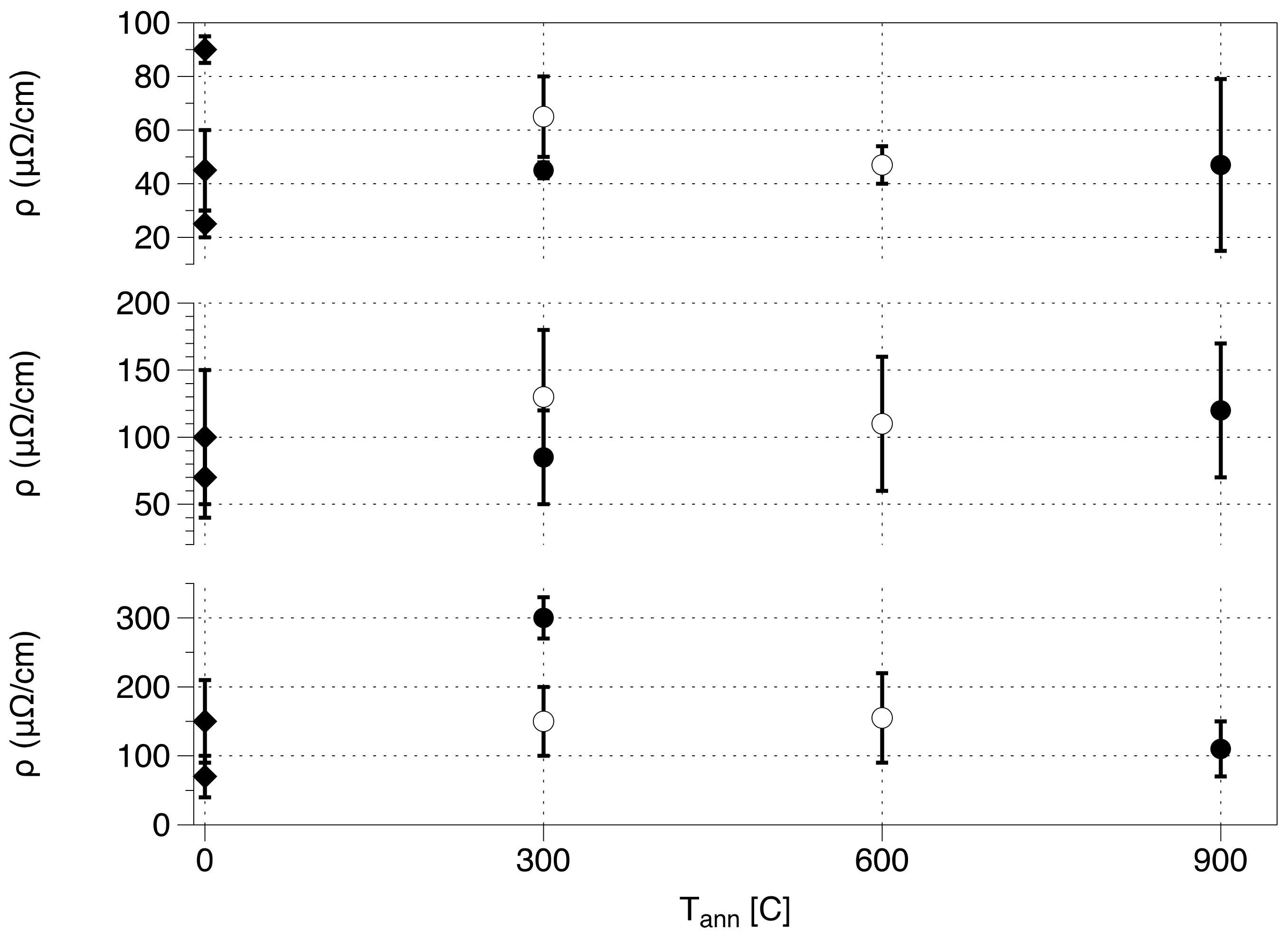
In Figure 1 we report the resistivity values as a function of the annealing temperature for different thickness. The graph points out that the resistivity is typically lower for the thinner films. Moreover, the annealing using higher temperatures does not show improvements for films with the lowest thicknesses, while some variability for the thickest one (900 nm) is present. As listed in Table 1 the lower resistivity values (40–45 μΩ∙cm) are achieved in films 300 nm thick. Still, reasonable values of resistivity are obtained in pristine films of 600 nm and 900 nm. Looking at Figure 1, it appears that temperature could be an important parameter only for thicker films and the lower values of resistivity are always associated with samples with no thermal treatment. The same behavior is observed if we change the holding time. The results of our study can be compared with the transport properties measured by Madhavi et al. [28] on oxidized metallic molybdenum films growth on a glass substrate. Madhavi et al. discussed the influence of the annealing temperature on the physical properties of molybdenum films having a thickness of 920–980 nm. After deposition, their films were characterized by an electrical resistivity of ~60 μΩ∙cm while, after annealing in air for three hours at different temperatures in the range of 473–673 K, a thermal oxidation occurred. The resistivity increased up to 83 μΩ∙cm at 473 K due to partial oxidation of Μο, and at 573 K it increased up to 200 μΩ∙cm. The further increase of the annealing temperature to 673 K increased the resistivity up to 320 μΩ∙cm.
The low resistivity of the as-deposited metallic Mo films reported in [28] is comparable with the values of our 900 nm thick films, including those annealed at 300 °C. On the contrary, at higher temperatures the resistivity values in Table 1 are lower mainly because we annealed the samples in high vacuum and, in this case, the transformation of the original metallic films to molybdenum oxides is a negligible or slower process.
Summarizing, for Mo films sputtered on the Al2O3 (0001) surface, the lowest resistivity is obtained for films ~300 nm thick. The thermal treatment in high vacuum may enhance the resistivity for a factor of two or three at the temperature of 900 °C for one or two hours, although resistivity values remain below 100 μΩ∙cm. This behavior can be associated with the rich variety of nanoscale structural, electronic, and magnetic phases coexisting in Mo films and in all transition metal films. The presence of these phases is at the origin of the mesoscopic and macroscopic behavior of films where different domains and, in particular, different oxide phases may occur. In our films the most important molybdenum stoichiometric oxides phases are MoO3 and MoO2. Bulk MoO3 is an insulating layered material, while molybdenum dioxide, characterized by a rutile structure is a metallic oxide with an electrical resistivity ranging from ~90 to 200 μΩ∙cm. Looking at Table 1 the resistivity of all but one is less than 200 μΩ∙cm. Since Mo films are heterogeneous media constituted of metallic and insulating domains, the percolation theory could be useful to calculate the relative resistivity [29] using, for example, random resistor networks. Indeed, the macroscopic conductivity in heterogeneous films is controlled by percolation phenomena. When the volume fraction Φ of the conducting phases (in this case Mo and MoO2) increases, the conductivity of the system increases. When it overcomes a critical value, called the percolation threshold (Φc), a network of pathways through the sample is formed and the conductivity tends to saturate. Accordingly, we may claim that these films contain limited amounts of insulating Mo oxide phases. The assessment of the type and amount of poorly-conductive phases in these films is challenging, but fundamental, to interpreting and possibly controlling the transport properties of thick Mo films or coatings for real applications. To this purpose, in addition to the transport experiments, we characterized our films also by X-ray absorption spectroscopy (XAS).
2.2. X-ray Absorption Spectroscopy Characterization
In these heterogeneous films XAS data can be usefully compared with transport experiments that return an average value at a definite temperature or the behavior vs. temperature. The behavior of the resistivity vs. thickness showed in Figure 1 confirms that Mo films grown through the sputtering process contain small amounts of insulating oxide phases. In the following we will discuss the characterization of the samples listed in Table 1 using the XAS technique performing experiments at the Mo K-edge. Consequently, to interpret the macroscopic behavior and to reproduce the effective conductivity of these films, it is necessary to identify the amount of the insulating phases present in each sample.
The XAS technique is a powerful method capable of investigating the local structural properties at the atomic level, such as geometry and coordination numbers in ordered and disorder systems, including surfaces, coatings, or interfaces, but also sensitive to the electronic structure [30]. XAS measurements were carried out at B18, the core XAS beamline of the Diamond Light Source, the UK synchrotron radiation facility operating at the electron energy of 3 GeV with a current of ~250 mA in the top-up mode. Spectra were collected using a double-crystal monochromator equipped with two Si (111) crystals and coupled to a Pt-coated mirror in the focusing mode illuminating the sample with a spot of ~200 μm × 200 μm [31]. This spot does not allow the resolution of a single phase domain, but simultaneously probes thousands of small domains. Indeed, these Mo metallic films are complex multiphase systems where molybdenum may exist in several oxidation states: Mo4+, Mo5+, and Mo6+. The thermal annealing in vacuum at moderate temperature does not affect the crystal structure, but may trigger the motion of oxygen atoms changing the oxygen contents and the oxidation state of Mo ions tuning the electrical conductivity. The acquisition of the Mo K-edge spectra has been performed in the continuous scan mode using a nine-element Ge detector with XSPRESS-II acquisition electronics in the fluorescence detection mode. XAS experiments have been performed at grazing incidence to enhance the signal associated to the surface layers of the Mo coatings to probe their structural composition. This approach was already discussed in a preliminary investigation of two relatively thick Mo films where the combined analysis of transport experiments and structural data showed that the amount of ordered phases play a limited role to the conductivity of these metallic films [15]. In that case the annealing at 300 °C slightly increased the conductivity. Actually, the conductivity of a Mo film may depend on the composition, the substrate, the morphology of the coatings, the oxygen content, the local order, the grain size, etc., and differences in the resistivity can be correlated also to the ratio between grain size and layer thickness [32].
Local Electronic Properties
XAS spectroscopy is a technique that, in addition to the local structure, probes the local and partial empty density of states around the photo-absorber. At the Mo K-edge we excite 1s core level electrons and, neglecting the possible correlation phenomena due to d electrons, the transition probes the p-projected empty density of states at the Mo site because of the dipole selection rule. Looking at the experimental spectra in Figure 2 and as discussed in [15] Mo K-edge spectra of these films are similar to the Mo metal spectrum and the small differences observed at the rising edge of each spectra points out tiny changes of the empty density of states of p character. In other words, the small difference in the partial empty density of states implies a different number of occupied electrons and a different hybridization [33]. In addition, the presence of a small shift of the K-edge points out a concurrent shift of the Fermi level, a parameter that can be correlated to the transport properties.
To this purpose, the comparison among spectra in Figure 2 is extremely interesting. In the two panels we compared the spectra of Mo films of different annealed thicknesses for one hour at 300 °C (left panel) and at 600 °C (right panel). At first sight all spectra are similar, pointing out that the local structure around molybdenum atoms is very similar. Weak changes appear only in the X-ray Absorption Near Edge Structure (XANES) region for samples annealed at 600 °C. However, after a careful normalization the differences among these spectra show a contribution near the edge that is correlated with the empty density of states of p and d character due to the contributions of dipolar and quadrupolar transitions, respectively. Taking as a reference the thicker films (900 nm), the empty density of states increases with thickness. The differences of the XAS spectra (green and brown curves) are in good agreement with the differences in the resistivity show in Table 1 (Figure 2 left panel: green ≥ 20 μΩ∙cm, brown ≥ 85 μΩ∙cm; Figure 2 right panel: green ≥ 45 μΩ∙cm, brown ≥ 105 μΩ∙cm). In fact, for these films the spectra shows a negligible amount of insulating oxide phases. The differences among the spectra demonstrates that the edge of the thicker films shifts slightly towards a lower energy, corresponding to a change of the Fermi energy actually compatible with a weak contribution of MoO3 (see the bottom panel in Figure 3).
As underlined above, the conductivity of Mo metallic films depends on many parameters. For this reason, for large scale applications, not only for high-performance accelerator components, is it important to characterize all properties: morphology, composition, structure and resistivity, and substrate. As an example, on crystalline substrates we may grow oriented films with a negligible strain and for thicknesses up to 600 nm with a resistivity <100–150 μΩ∙cm. In this framework, in recent years, modeling and simulation tools have become more and more important, being effective alternatives to long and costly experimental tests. However, for improved RF devices, it is mandatory to study the growth of Mo films not only on oriented surfaces of insulating or semiconductor substrates as discussed above, but on metallic substrates, such as copper.
We deposited Mo films by sputtering on oxygen-free high thermal conductivity (OFHC) copper surfaces with a high roughness (~700 nm). Atomic force microscopy (AFM, MSNL-10 of Veeco Instruments, New York, NY, USA) images showed that the surface morphology of the Mo coatings preserve the initial roughness, and even without annealing, the molybdenum layer may slightly improve the original roughness. However, since Cu and Mo have different crystal structures (f.c.c. vs. b.c.c.) and different thermal expansion coefficients, the Mo layer deposited on top of the Cu surface changes with temperature and its structure above 900 °C. We investigated the deposition of thin Mo layers sputtered on Cu surfaces annealed at 750 °C for 10 min [5]. A previous study pointed out that a sputtering thickness of 180 nm is not suitable enough to obtain a homogeneous coating surface and, due to the low contacting force and the intense thermal stress, this thin coating annealed at 600 °C for two hours shows a clear separation of the Mo layer from the substrate. Indeed, the thermal expansion coefficients of Cu and Mo are quite different, i.e., 16 × 10−6 and 5 × 10⁻⁶ μm/m/°C, respectively. Rutherford backscattering spectrometry (RBS, 3.5 MeV Singletron accelerator, High Voltage Engineering Europa B.V., Amersfoort, The Netherlands) experiments performed with a 4He+ ion beam characterized the depth profile of Mo on the Cu substrates [5]. Data showed an inter-diffusion of the Mo at the Cu-Mo interface, a process that tend to form a homogeneous mixture at the interface not observed for films growth on SiO2 or Al2O3. RBS also pointed out a Mo concentration lower than a pure Mo film, a behavior compatible with the presence of oxide phases in the deposited film. The non-uniform oxygen distribution and the resistivity, the latter higher by about two orders of magnitude compared to a pure film of Mo, are also compatible with the presence of insulating oxide phases [5].
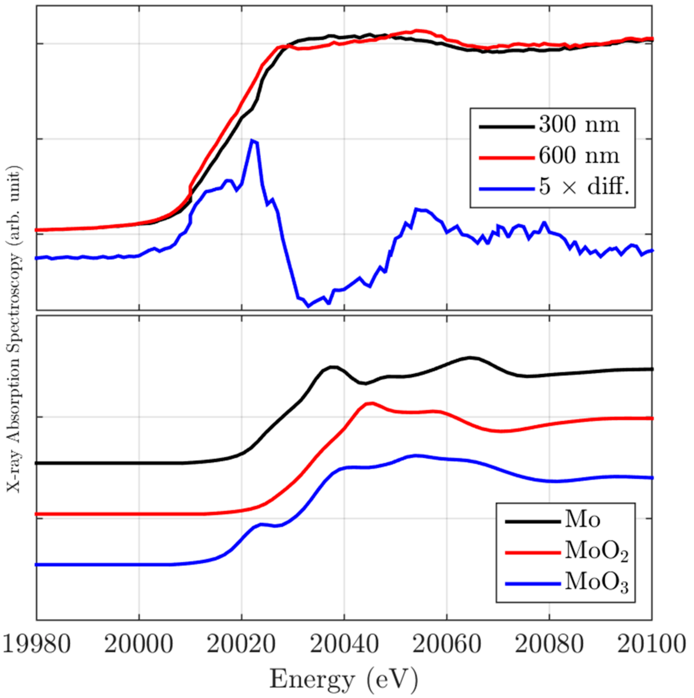
These Mo metallic films are more heterogeneous and disordered than those grown by magnetron sputtering on Al2O3 substrates, as shown in Figure 3 (upper panel), where we compare the XAS spectra at the K-edge of Mo of two films of ~300 nm and ~600 nm grown on a clean OFHC Cu surface. The spectrum of the 300 nm film is characterized at the edge by a very broad feature, characteristic of a strongly-disordered local structure, while the spectrum of the 600 nm film starts to show the typical shape of Mo metal with a shift of 1.5 (±0.2) eV towards low energy, which points out a lowering of the Fermi level with respect to the thinner disordered Mo film. The difference (blue curve) clearly points out a significant enhancement of the empty density of states in the 300 nm disordered film, compatible with a small contribution from insulating oxide phases.
To clarify the behavior of the XANES spectra of the Mo film grown on Al2O3 and copper substrates, we simulated the Mo K-edge XANES spectra of Mo metal and of the two main oxide phases: MoO2 and MoO3. Spectra were simulated using the full multiple scattering (FMS) theory as implemented in FEFF9.6 code [34]. The self-consistent field (SCF) method was employed for potential calculations with Hedin-Lundqvist exchange and correlation potential. The radius of atomic clusters for SCF and FMS calculations are, respectively, 5 Å and 10 Å. The crystallographic structures were adopted as starting models. Neither an additional energy shift nor extra broadening convolution were applied in all calculations. In Figure 3 (bottom panel) are compared to the simulated XANES spectra of the main oxides phases (MoO2 metallic and MoO3 insulating). Both spectra are different from the spectra of Mo coatings, in agreement with the description of these films: heterogeneous systems containing metallic domains and negligible contributions of insulating oxide phases.
3. Discussion
As discussed in the introduction, new accelerator projects need improved RF structures for which important research and development to reduce pulse heating effects and electrical breakdown is required. A possible route is represented by the improvement of devices manufactured in OFHC copper by deposition of suitable coatings, e.g., molybdenum, ruthenium, or other refractory material with high electrical conductivity and good mechanical properties. Alternatively, alloys or multilayer networks based on transition metal (TM) oxides whose microstructure, thermal behavior, and chemistry are compatible with the long term operation of RF devices and their fabrication methods. References are available, but the scenario of possible metal/metal combinations is limited. Only a recent work deals with the case of TM oxides grown on transition metals, in particular Mo and TM oxides [35].
This study has focused on the development of innovative technologies based on Mo coatings on copper in order to raise the discharge electrical threshold (i.e., the breakdown) and/or in alternative, to reduce the damage due to breakdown phenomena.
The results we obtained point out that Mo coatings are multiphase metallic films with negligible contributions of insulating oxide phases. The experiments show that the increased thickness electronics changes can be associated with changes of the conductivity, whose values are better than the conductive MoO2. However, as showed in Figure 3 (upper panel), Mo metallic films grown on a clean OFHC Cu surface are more heterogeneous and disordered than those grown on Al2O3 substrates. Although data show that the coating option offers suitable conductivity values and RF devices with Mo coatings could be manufactured, a lot of research and development is still necessary to achieve the performance required by operations at high power.
In addition to the electrical conductivity, to optimize the performance of high field gradient devices, the reduction of field emission dark current from the metal surface is also important. Indeed, in the worst case, the increase of the dark current is a marker of an electrical breakdown, and the start of the degradation of performance. In the case of Mo, a deeper understanding of the field emission from its surfaces, naturally-oxidized and/or heated, is required. Recently, Lagotzky et al. [36] showed that well-polished Mo samples did not show parasitic field emission up to a field level of 50 MV/m, while in situ heat treatments above 400 °C activated the field emission at lower field strength. However, oxygen loading into the Mo surface partially weakens the emitters revealing the suppression of field emission by native Mo oxides. Taking into account experiments that reported the decrease of the field effect from a Mo oxidized surface and the formation of islands of MoO3, the Mo oxide phase diagram and the interaction in a metal/metal substrate pair, an interesting composition to investigate in the future is the Cu/MoO3 pair. Indeed thin “insulating” layers of MoO3 maintain a high work function (~7 eV) while becoming conductive on a Cu substrate [35].
4. Conclusions
The design of RF devices suitable to minimize breakdown, which limits the high gradient performance of these structures, depends on the materials, surface processing techniques, and also the geometry. It is then necessary understand and predict the breakdown behavior of practical structures, but at the same time investigate alternative highly-performing materials in terms of breakdown. Actually, after decades of studies and experiments, dedicated studies, and a specific research and development launched in this field in the linear-collider community, the high-gradient RF breakdown phenomenon remains an open problem [37]. At present, depending on the properties of the surface material, breakdown phenomena in vacuum typically occurs for accelerating gradients >100 MV/m. The foreseen goal is to achieve accelerating gradients much higher than this value using standard accelerating structures and practical operating conditions. To this purpose we attempted to identify new materials or alloys to improve the performances of copper using metallic coatings. Indeed, using advanced manufacturing techniques combining precision electroforming and film deposition, new possibilities for RF devices may open. Adding a Mo metallic layer, of which we may control the composition, internal stress, mechanical properties, roughness, etc., properties of copper, like the thermo-mechanical stability, may be improved, reaching values not attainable with uncoated copper.
With this research we characterized relatively thick films of Mo grown on copper to improve and optimize performance. Compared to Cu, the Mo conductivity is lower, however, the relatively high-conductivity of Mo metallic coatings and the higher Mo breakdown rate make its application in high-gradient accelerating structures an interesting and useful option [13,14,15,38]. Moreover, we show that, by using X-ray absorption spectroscopy, we can control the presence of insulating oxide phases and correlate the electronic properties with the conductivity properties of these films. However, due to the properties of transition metal oxides grown on metallic substrates, new ideas are emerging. In particular, a large amount of interest is devoted to metallic molybdenum oxides due to their mechanical resistance, good electrical conductivity, and low field emission.
Acknowledgments
Part of this research was undertaken within the in house research program at the Diamond Light Source, the UK national synchrotron radiation facility. One of us (S.M.) acknowledges the Roma Tre University for financial support during his stage at Diamond. W.X. acknowledges financial support from NSFC (grant No. U1532128).
Author Contributions
A.M. and B.S. conceived and designed the experiments; A.M., G.C., and S.S. performed the experiments; W.X. performed the XANES calculations. All authors contributed to data analysis and to writing the manuscript. All authors have read and approved the final manuscript.
Conflicts of Interest
The authors declare no conflict of interest.
References
- Grudiev, A.; Calatroni, S.; Wurnsh, W. New local field quantity describing the high gradient limit of accelerating structures. Phys. Rev. Accel. Beams 2009, 12, 102001. [Google Scholar] [CrossRef]
- Higo, T.; Higashi, Y.; Matsumoto, S.; Yokoyama, K.; Tsukuba, K.E.K.; Doebert, S.; Grudiev, A.; Riddone, G.; Wuensch, W.; et al. Advances in X-band TW accelerator structures operating in the 100 MV/m regime. In Proceedings of the International Particle Accelerator Conference, Kyoto, Japan, 23–28 May 2010; pp. 3810–3812. [Google Scholar]
- Wuensch, W. CLIC accelerating structure development. In Proceedings of the 11th European Particle Accelerator Conference, Genoa, Italy, 23–27 June 2008. [Google Scholar]
- Antoine, C.Z.; Peauger, F.; Le Pimpec, F. Electromigration occurrences and its effects on metallic surfaces submitted to high electromagnetic field: A novel approach to breakdown in accelerators. Nucl. Instrum. Methods Phys. Res. Sect. A 2011, 665, 54–69. [Google Scholar] [CrossRef]
- Bini, S.; Chimenti, V.; Marcelli, A.; Palumbo, L.; Spataro, B.; Dolgashev, V.; Tantawi, S.; Yeremian, A.D.; Higashi, Y.; Grimaldi, M.G.; et al. Development of X-band accelerating structures for high gradients. Chin. Phys. C 2012, 36, 639–647. [Google Scholar] [CrossRef]
- Dolgashev, V.A.; Gatti, G.; Higashi, Y.; Leonardi, O.; Lewandowski, J.R.; Marcelli, A.; Rosenzweig, J.; Spataro, B.; Tantawi, S.G.; Yeremian, D.A. High power tests of an electroforming cavity operating at 11.424 GHz. J. Inst. 2016, 11, P03010. [Google Scholar]
- Gatti, G.; Marcelli, A.; Spataro, B.; Dolgashev, V.; Lewandowski, J.; Tantawi, S.G.; Yeremian, A.D.; Higashi, Y.; Rosenzweig, J.; Sarti, S.; et al. X-band accelerator structures: On going R & D at the INFN. Nucl. Instrum. Methods Phys. Res. Sect. A 2016, 829, 206–212. [Google Scholar]
- Laurent, L.; Tantawi, S.; Dolgashev, V.; Nantista, C.; Higashi, Y.; Aicheler, M.; Heikkinen, S.; Wuensch, W. Experimental study of rf pulsed heating. Phys. Rev. Accel. Beams 2011, 14, 041001. [Google Scholar] [CrossRef]
- Dolgashev, V.; Tantawi, S.; Higashi, Y.; Spataro, B. Geometric dependence of radio-frequency breakdown in normal conducting accelerating structures. Appl. Phys. Lett. 2010, 97, 171501. [Google Scholar] [CrossRef]
- Tantawi, S.; Dolgashev, V.; Higashi, Y.; Spataro, B. Research and Development for Ultra-High Gradient Accelerator Structures. AIP Conf. Proc. 2010, 1299. [Google Scholar] [CrossRef]
- Graedel, T.E.; Harper, E.M.; Nassar, N.T.; Reck, B.K. On the materials basis of modern society. Proc. Natl. Acad. Sci. USA 2015, 112, 6295–6300. [Google Scholar] [CrossRef] [PubMed]
- Darling, K.A.; Rajagopalan, M.; Komarasamy, M.; Bhatia, M.A.; Hornbuckle, B.C.; Mishra, R.S.; Solanki, K.N. Extreme creep resistance in a microstructurally stable nanocrystalline alloy. Nature 2016, 537, 378–381. [Google Scholar] [CrossRef] [PubMed]
- Bini, S.; Spataro, B.; Marcelli, A.; Sarti, S.; Dolgashev, V.A.; Tantawi, S.; Yeremian, A.D.; Higashi, Y.; Grimaldi, M.G.; Romano, L.; et al. Molybdenum sputtering film characterization for high gradient accelerating structures. Chin. Phys. C 2013, 37, 097005. [Google Scholar] [CrossRef]
- Xu, Y.; Spataro, B.; Sarti, S.; Dolgashev, V.A.; Tantawi, S.; Yeremian, A.D.; Higashi, Y.; Grimaldi, M.G.; Romano, L.; Ruffino, F.; et al. Structural and morphological characterization of Mo coatings for high gradient accelerating structures. In Proceedings of the 15th International Conference on X-ray Absorption Fine Structure (XAFS15), Beijing, China, 22–28 July 2012. [Google Scholar]
- Marcelli, A.; Spataro, B.; Sarti, S.; Dolgashev, V.A.; Tantawi, S.; Yeremian, D.A.; Higashi, Y.; Parodi, R.; Notargiacomo, A.; Xu, J.; et al. Characterization of thick conducting molybdenum films: Enhanced conductivity via thermal annealing. Surf. Coat. Technol. 2015, 261, 391–397. [Google Scholar] [CrossRef]
- Fowler, R.H.; Nordheim, L. Electron Emission in Intense Electric Fields. R. Soc. Publ. 1928, 119, 173–181. [Google Scholar] [CrossRef]
- Furuta, F.; Nakanishi, T.; Okumi, S.; Gotou, T.; Yamamoto, M.; Miyamoto, M.; Kuwahara, M.; Yamamoto, N.; Naniwa, K.; Yasui, K.; et al. Reduction of field emission dark current for high-field gradient electron gun by using a molybdenum cathode and titanium anode. Nucl. Instrum. Methods Phys. Res. Sect. A 2005, 538, 33–44. [Google Scholar] [CrossRef]
- Chimenti, P.; Caliendo, C.; Spataro, B. A Procedure to Obtain a Very Low Mo films with Oxygen Contamination. SPARC 2012. Available online: http://www.lnf.infn.it/acceleratori/sparc/TECHNOTES/RF/SPARC_RF_12_004.pdf (accessed on 28 November 2013).
- Schmid, U.; Seidel, H. Effect of substrate properties and thermal annealing on the resistivity of molybdenum thin films. Thin Solid Films 2005, 489, 310–319. [Google Scholar] [CrossRef]
- Rafaja, D.; Köstenbauer, H.; Mühle, U.; Löffler, C.; Schreiber, G.; Kathrein, M.; Winkler, J. Effect of the deposition process and substrate temperature on the microstructure defects and electrical conductivity of molybdenum thin films. Thin Solid Films 2013, 528, 42–48. [Google Scholar] [CrossRef]
- Glebovsky, V.G.; Markaryans, E.A. Thin film metallization by magnetron sputtering from highly pure molybdenum targets. J. Alloy. Compd. 1993, 190, 157–160. [Google Scholar] [CrossRef]
- Descoeudres, A.; Ramsvik, T.; Calatroni, S.; Taborelli, M.; Wuensch, W. Dc breakdown conditioning and breakdown rate of metals and metallic alloys under ultrahigh vacuum. Phys. Rev. Spec. Top. Accel. Beams 2009, 12, 032001. [Google Scholar] [CrossRef]
- Sondheimer, E.H. The mean free path of electrons in metals. Adv. Phys. 2001, 50, 499–537. [Google Scholar] [CrossRef]
- Harrison, K.W.; Corolewski, C.D.; McCluskey, M.D.; Lindemuth, J.; Ha, S.; Norton, M.G. Electronic transport in molybdenum dioxide thin films. J. Mater. Sci. Mater. Electron. 2015, 26, 9717–9720. [Google Scholar] [CrossRef]
- Alonzo-Medina, G.M.; González-González, A.; Sacedón, J.L.; Oliva, A.I. Understanding the thermal annealing process on metallic thin films. IOP Conf. Ser. Mater. Sci. Eng. 2013, 45, 012013. [Google Scholar] [CrossRef]
- Tosoratti, N.; Fastampa, R.; Giura, M.; Lenzi, V.; Sarti, S.; Silva, E. Two techniques for broadband measurement of the surface impedance of high critical temperature superconducting thin films. Int. J. Mod. Phys. B 2000, 14, 2926–2931. [Google Scholar] [CrossRef]
- Ganchev, S.; Qaddoumi, N.; Bakhtiari, S.; Zoughi, R. Calibration and measurement of dielectric properties of finite thickness composite sheets with open-ended coaxial sensors. IEEE Trans. Instrum. Meas. 1995, 44, 1023–1029. [Google Scholar] [CrossRef]
- Madhavi, V.; Kondaiah, P.; Rayudu, S.S.; Hussain, O.M.; Uthanna, S. Properties of MoO3 films by thermal oxidation: Annealing induced phase transition. Mater. Express 2013, 3, 135–143. [Google Scholar] [CrossRef]
- Kirkpatrick, S. Percolation and Conduction. Rev. Mod. Phys. 1973, 45, 574–588. [Google Scholar] [CrossRef]
- Bianconi, A.; Marcelli, A. Surface XANES. In Synchrotron Radiation Research. Advances in Surface Science; Bachrach, R.Z., Ed.; Plenum Press: New York, NY, USA, 1992; Volume 1. [Google Scholar]
- Dent, J.; Cibin, G.; Ramos, S.; Parry, S.A.; Gianolio, D.; Smith, A.D.; Scott, S.M.; Varandas, L.; Patel, S.; Pearson, M.R.; et al. Performance of B18, the Core EXAFS Bending Magnet beamline at Diamond. J. Phys. Conf. Ser. 2013, 430, 012023. [Google Scholar] [CrossRef]
- Muecke, U.P.; Graf, S.; Rhyner, U.; Gauckler, L.J. Microstructure and electrical conductivity of nanocrystalline nickel and nickel oxide/gadolinia-doped ceria thin films. Acta Mater. 2008, 56, 677–687. [Google Scholar] [CrossRef]
- Xu, W.; Liu, Y.; Zhao, L.; An, P.; Lin, Y.; Marcelli, A.; Wu, Z. Evidence of an interlayer charge transfer route in BiCu1−xSeO. J. Mater. Chem. A 2013, 1, 12154–12158. [Google Scholar] [CrossRef]
- Rehr, J.J.; Kas, J.J.; Vila, F.D.; Prange, M.P.; Jorissen, K. Parameter-free calculations of X-ray spectra with FEFF9. Phys. Chem. Chem. Phys. 2010, 12, 5503–5513. [Google Scholar] [CrossRef]
- Greiner, M.T.; Chai, L.; Helander, M.G.; Tang, W.; Lu, Z. Transition metal oxide work functions: The influence of cation oxidation state and oxygen vacancies. Adv. Funct. Mater. 2012, 22, 4557–4568. [Google Scholar] [CrossRef]
- Lagotzky, S.; Barday, R.; Jankowiak, A.; Kamps, T.; Klimm, C.; Knobloch, J.; Müller, G.; Senkovskiy, B.; Siewert, F. Prevention of electron field emission from molybdenum substrates for photocathodes by the native oxide laye. Eur. Phys. J. Appl. Phys. 2015, 70. [Google Scholar] [CrossRef]
- Why We Need Compact Linear Collider. Available online: http://clic-study.org (accessed on 6 April 2017).
- Castorina, G.; Marcelli, A.; Monforte, F.; Sarti, S.; Spataro, B. An analytical model for evaluating the properties of metallic coatings in RF structures. Condens. Matter 2016, 1, 12. [Google Scholar] [CrossRef]
Figure 1.
Resistivity values as a function of annealin g temperature for films of different thicknesses, (Top panel) d = 300 nm; (Middle panel) d = 600 nm; (Bottom panel) d = 900 nm. For Tann > 0, different symbols represent different holding times (HT): empty dots, HT = 1 h; filled dots, HT = 2 h (data from Table 1). Diamonds represent samples that did not undergo thermal treatment.

Figure 2.
(Left panel) comparison of Mo K-edge spectra of samples of 300 nm, 600 nm, and 900 nm annealed at 300 °C for 1 h. The bottom curves are the differences between spectra of different thickness (multiplied 5×); (Right panel) the same as in the left panel for the samples with the same thickness, but annealed at 600 °C for 1 h.
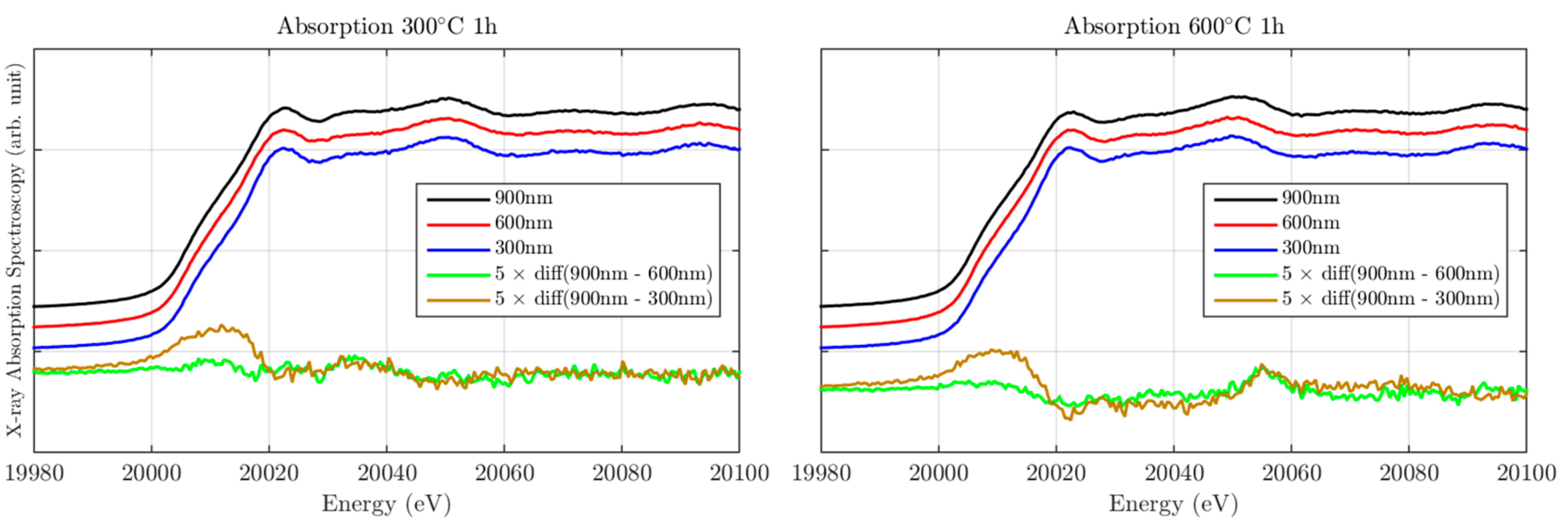
Figure 3.
(Top panel) comparison of Mo K-edge XANES spectra of two Mo films: 300 nm and 600 nm thick grown on OFHC copper substrates. The blue curve is the difference between the two experimental spectra multiplied by five to enhance the difference at the edge (see text); (Bottom panel) comparison among Mo K-edge XANES spectra of Mo metal (black), MoO2 (red), and MoO3 (blue) simulated using the full multiple scattering (FMS) theory (see text).

Table 1.
Parameters of the Mo films grown on Al2O3 (0001).
| N | D (nm) | Tann (°C) | Holding Time (h) | ρ (μΩ∙cm) | δρ 1 |
|---|---|---|---|---|---|
| 1 | 300 | 0 | 0 | 25 | 5 |
| 2 | 600 | 0 | 0 | 70 | 30 |
| 3 | 900 | 0 | 0 | 70 | 30 |
| 4 | 300 | 300 | 2 | 45 | 3 |
| 5 | 600 | 300 | 2 | 85 | 35 |
| 6 | 900 | 300 | 2 | 300 | 30 |
| 7 | 300 | 0 | 0 | 45 | 15 |
| 8 | 300 | 0 | 0 | 90 | 5 |
| 9 | 300 | 300 | 1 | 65 | 15 |
| 10 | 300 | 600 | 1 | 47 | 7 |
| 11 | 300 | 900 | 2 | 47 | 32 |
| 12 | 600 | 0 | 0 | 100 | 50 |
| 13 | 600 | 300 | 1 | 130 | 50 |
| 14 | 600 | 600 | 1 | 110 | 50 |
| 15 | 600 | 900 | 2 | 120 | 50 |
| 16 | 900 | 0 | 0 | 150 | 60 |
| 17 | 900 | 300 | 1 | 150 | 50 |
| 18 | 900 | 600 | 1 | 155 | 65 |
| 19 | 900 | 900 | 2 | 110 | 40 |
1 δρ is the error corresponding to the half-width of the difference (ρmax–ρmin).
© 2017 by the authors. Licensee MDPI, Basel, Switzerland. This article is an open access article distributed under the terms and conditions of the Creative Commons Attribution (CC BY) license (http://creativecommons.org/licenses/by/4.0/).
Share and Cite
MDPI and ACS Style
Marcelli, A.; Spataro, B.; Castorina, G.; Xu, W.; Sarti, S.; Monforte, F.; Cibin, G. Materials and Breakdown Phenomena: Heterogeneous Molybdenum Metallic Films. Condens. Matter 2017, 2, 18. https://doi.org/10.3390/condmat2020018
AMA Style
Marcelli A, Spataro B, Castorina G, Xu W, Sarti S, Monforte F, Cibin G. Materials and Breakdown Phenomena: Heterogeneous Molybdenum Metallic Films. Condensed Matter. 2017; 2(2):18. https://doi.org/10.3390/condmat2020018
Chicago/Turabian StyleMarcelli, Augusto, Bruno Spataro, Giovanni Castorina, Wei Xu, Stefano Sarti, Francesca Monforte, and Giannantonio Cibin. 2017. "Materials and Breakdown Phenomena: Heterogeneous Molybdenum Metallic Films" Condensed Matter 2, no. 2: 18. https://doi.org/10.3390/condmat2020018