High Gauge Factor Piezoresistors Using Aluminium Induced Crystallisation of Silicon at Low Thermal Budget †

School of Electrical Engineering and Telecommunications, University of New South Wales, Sydney 2052, Australia
*
Author to whom correspondence should be addressed.
†
Presented at the Eurosensors 2017 Conference, Paris, France, 3–6 September 2017.
Proceedings 2017, 1(4), 354; https://doi.org/10.3390/proceedings1040354
Published: 5 September 2017
(This article belongs to the Proceedings of Proceedings of Eurosensors 2017, Paris, France, 3–6 September 2017)
Abstract
:This paper reports on polysilicon piezo-resistors that are fabricated at a low thermal budget using aluminium-induced-crystallization (AIC) of ultra-high-vacuum e-beam evaporated silicon films. By in-situ phosphorus doping of precursor amorphous silicon films e-beam evaporated at room temperature on aluminium layer, we are able to increase and control the gauge factor of the polysilicon films formed by AIC at 450 °C. Piezo-resistors made from the polysilicon films are integrated on microcantilever beams to measure their gauge factors. Gauge factors as high as 62 is obtained for 2 × 10¹⁸/cm3 phosphorus doping level in the precursor amorphous silicon film. The measured gauge factors are significantly higher than previously reported values for polysilicon films.
1. Introduction
Fabricating sensors and actuators at low thermal budget is necessary for post CMOS-MEMS integration. Existing silicon piezo-resistors are typically made by diffusion or ion-implantation of dopants into single or polycrystalline silicon. In-situ doping of epitaxially grown c-silicon and LPCVD polysilicon are also demonstrated for fabricating silicon piezo-resistors. However, these processes require high temperature making them incompatible with post CMOS-MEMS integration. AIC polysilicon films formed at temperatures less than 550 °C is commonly used for solar cell applications [1]. But, their use for piezo-resistive applications has been limited due to the formation of polysilicon films with small gauge factor of less than 20 [2,3]. This may be attributed to the formation of small grain size and fixed Al doping of 2.8 × 10¹⁸/cm3 in the AIC polysilicon films. In this paper, we report the enhancement of the gauge factor of AIC polysilicon film (formed at 450 °C) by in-situ phosphorus doping of the precursor amorphous silicon that is e-beam evaporated at ultra-high vacuum.
2. Experiment
Precursor amorphous silicon films of 500 nm thick with phosphorus doping of 1 × 10¹⁶/cm3 (intrinsic), and 2 × 10¹⁸/cm3 are evaporated using e-beam on Al (300 nm)/SiO2 (700 nm)/Si (bulk) under room temperature and at base pressure of 1 × 10⁻⁸ Torr at a deposition rate of 30 nm/min. Upon annealing in dry N2 ambience at 450 °C for 2 h, a continuous polysilicon film is formed underneath the aluminium layer through the process of aluminium induced crystallization [1].
The aluminium layer is then removed with standard aluminium etch and the continuous silicon is exposed by mechanical polishing to remove the excess silicon on top. The crystal properties, relative aluminium and phosphorous concentrations, and sheet resistance of the AIC silicon films are studied using EBSD, TF-SIMS, and four point probe measurements, respectively. The films are then defined and etched to form a piezo-resistor, which is further integrated with a cantilever to measure its gauge factor. The fabrication process for the AIC silicon and formation and integration of piezo-resistor is presented in Figure 1a. Figure 1b shows the photo of released cantilever integrated with AIC piezo-resistor taken under microscope.
The released cantilevers are then strained and the resulting radii of curvature are measured. The gauge factors of the films are calculated using the following equation.
where ρ and h are the radius of curvature and thickness of the strained cantilever, respectively. ΔR and R stand for the change in the polysilicon resistance and the unstrained polysilicon resistance value.
3. Results and Discussion
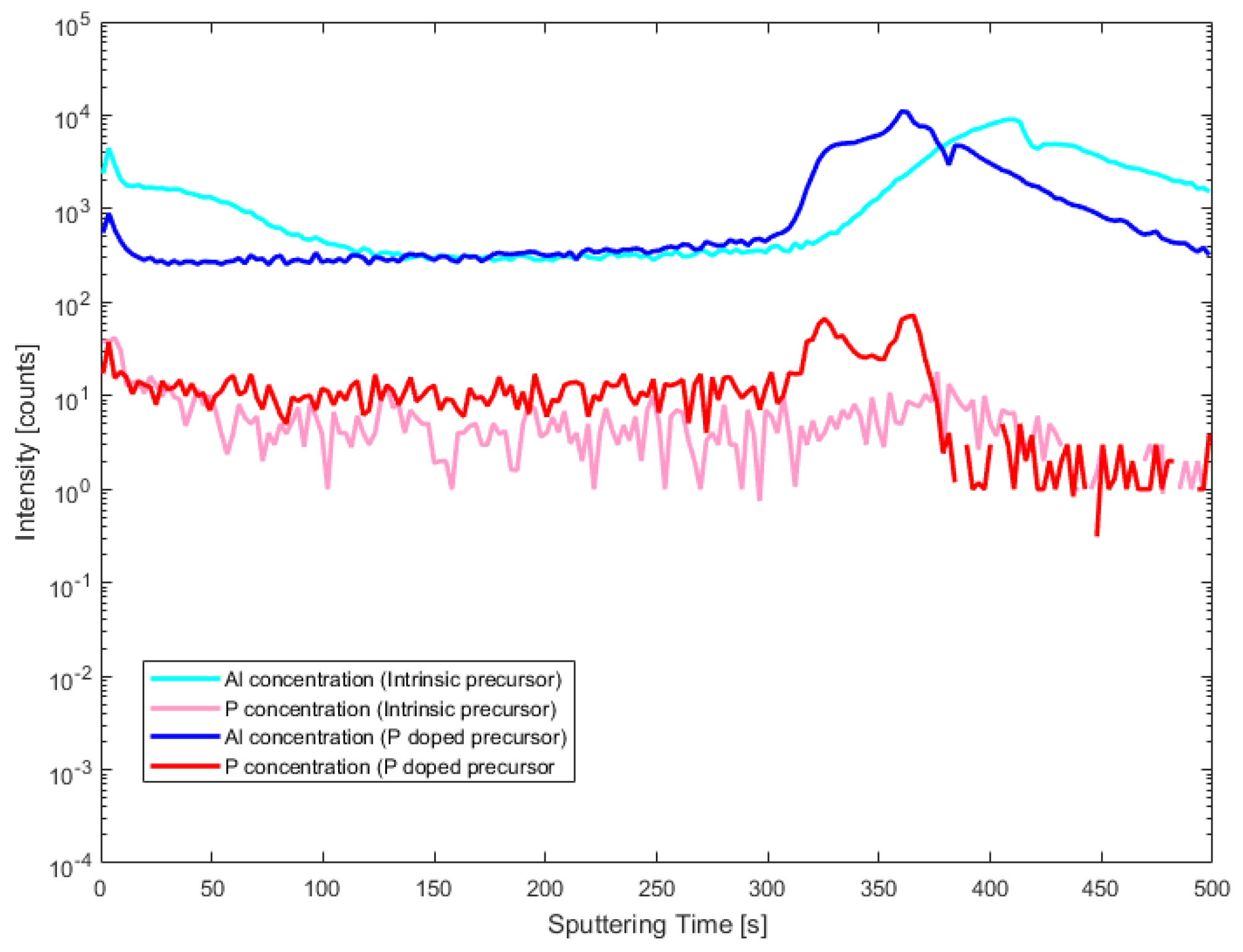
The relative aluminium and phosphorus concentrations in the AIC polysilicon films measured using TF-SIMS is plotted in Figure 2. It shows that the aluminium concentration remains unchanged in the intrinsic and the phosphorus doped cases. From previous study [1], the aluminium concentration in the intrinsic case is estimated to be 2.8 × 10¹⁸/cm3. However, the phosphorus concentration in the AIC polysilicon increases as more phosphorus doping is introduced into the precursor.
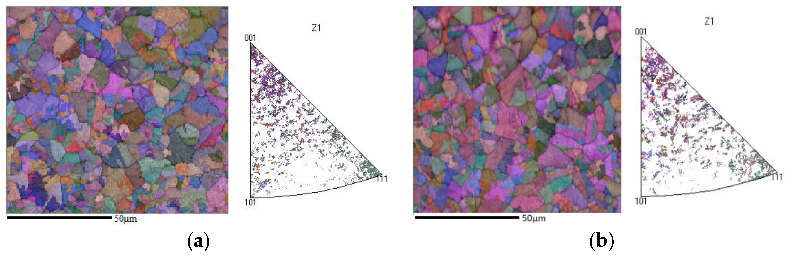
The crystal properties of the silicon grains formed under AIC was studied using EBSD and the preferred crystal orientations were plotted on an inverse pole in Figure 3. From the EBSD measurement, the average grain size for the intrinsic precursor was 8 µm while the grain size for the doped case was slightly higher at 8.3 µm. The dominant crystal orientations are (100) and (111) in both cases. The effect of phosphorus doping contributing to the change in grain sizes of AIC polysilicon is minimal. Also, phosphorous doping does not seem to influence crystal orientations significantly.
The sheet resistance, as shown in Table 1, increases from 686 Ω/□ for intrinsic precursor to 848 Ω/□ for a precursor with phosphrous doping of 2 × 10¹⁸/cm3. Since the effect of phosphrous doping on grain size and crystal orientations is not significant, the increase in sheet resistance is likely due to the counter doping effect that phosphrous in the precusor has on the carrier levels in the formed AIC polysilicon. The increase in sheet resistance indicates the decrease in carrier level in the AIC films as doped by n-type phosphrous carrier. The decrease in carrier level in silicon film is expected to result in an increase in piezo-resistivity, which needs to be confirmed by studying the piezo-resistive behavior of the AIC polysilicon films.
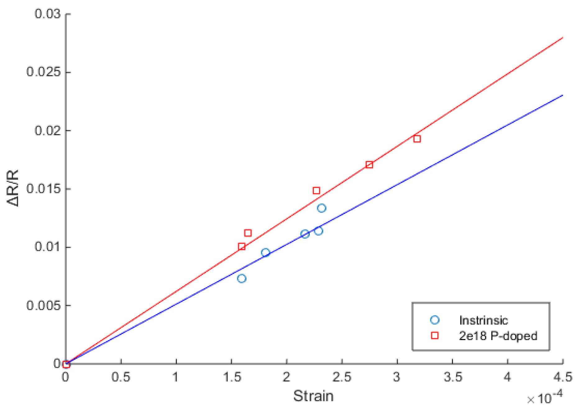
The piezoresitivity of the AIC polysilicon films is characterized by measuring gauge factor of the resistors that are integarted with released cantilever. The measured change in resitances at various strain levels are plotted in Figure 4 for the intrinsic and phosphrous doping of 2 × 10¹⁸/cm3. The gauge factors were extracted from the Figure 4 using the line of best fit. A 19% increase in gauge factor was observed from the intrinsic case of 52 to 62 for the phosphrous doping of 2 × 10¹⁸/cm3 as shown in Table 2.
Comparing with previous AIC polysilicon films and LPCVD polysilicon films [4], a relatively large gauge factor was obtained. This increase in gauge factor is mainly due to a large polysilicon grain size. The gauge factor can then be further increased by introducing phosphorus doping to the precursor to decrease the majority carrier concentration.
4. Conclusions
Polysilicon films with large piezo-resistive characteristic have been fabricated at low thermal budget. In situ phosphorous doping of e-beam evaporated amorphous silicon film is used as a precursor in aluminium induced crystallization to form a polysilicon film with improved and controlled piezo-resistive property. With phosphorus doping of 2 × 10¹⁸/cm3 in the precursor, a polysilicon film with a gauge factor of 62 is obtained at maximum processing temperature of 450 °C. This is larger than any of the polysilicon films reported thus far. The large gauge factor may be attributed to large average grain size and counter doping effect due to in situ phosphorous doping.
Acknowledgments
The authors acknowledge the School of Electrical Engineering and Telecommunications UNSW, School of Photovoltaic and Renewable Energy UNSW, Australian National Fabrication Facility, NSW node where the devices where fabricated and the Electron Microscope Unit UNSW, where the measurements took place.
Conflicts of Interest
The authors declare no conflict of interest.
References
- Nast, O.; Wenham, S.R. Elucidation of the layer exchange mechanism in the formation of polycrystalline silicon by aluminum-induced crystallization. J. Appl. Phys. 2000, 88, 124–132. [Google Scholar] [CrossRef]
- Uhlig, S.; Rau, S.; Schultes, G. Piezoresistivity of polycrystalline silicon applying the AIC process-route. Sens. Actuators A Phys. 2011, 172, 447–454. [Google Scholar] [CrossRef]
- Patil, S.K.; Çelik-Butler, Z.; Butler, D.P. Piezoresistive polysilicon film obtained by low-temperature aluminum-induced crystallization. Thin Solid Films 2010, 519, 479–486. [Google Scholar] [CrossRef]
- French, P.J.; Evans, A.G.R. Piezoresistance in polysilicon and its applications to strain gauges. Solid State Electron. 1989, 32, 1–10. [Google Scholar] [CrossRef]
Figure 1.
(a) Fabrication process of AIC polysilicon and the test structure; (b) Optical image of the cantilever with polysilicon on top.
Figure 1.
(a) Fabrication process of AIC polysilicon and the test structure; (b) Optical image of the cantilever with polysilicon on top.
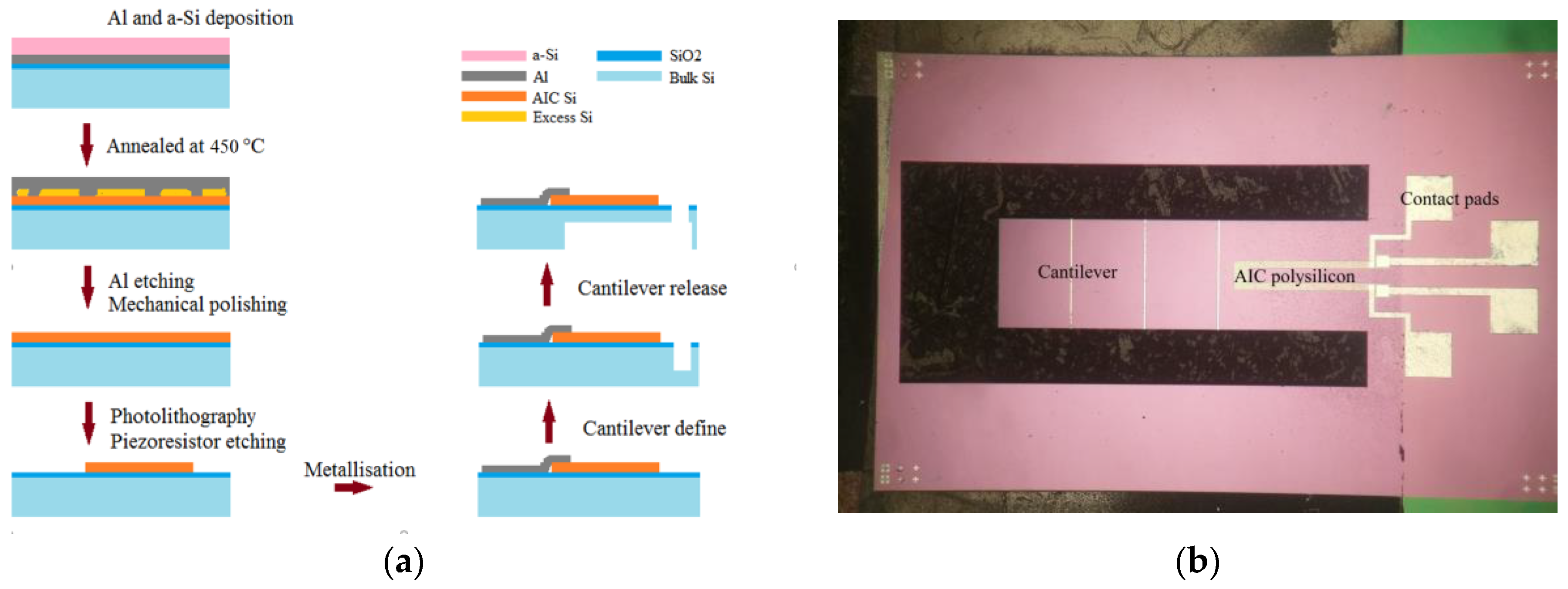
Figure 2.
TF-SIMS measurement of doped AIC polysilicon.

Figure 3.
(a) EBSD of intrinsic precursor; (b) EBSD of 2 × 10¹⁸/cm3 phosphorus doped precursor.

Figure 4.
Change in resistance against strain.


Table 1.
Sheet resistance.
| Doping | Intrinsic | 2 × 10¹⁸/cm3 |
|---|---|---|
| Sheet Resistance [Ω/sq] | 686 | 840 |
Table 2.
Measured gauge factor.
| Doping | Intrinsic | 2 × 10¹⁸/cm3 |
|---|---|---|
| Gauge Factor | 52 | 62 |
Publisher’s Note: MDPI stays neutral with regard to jurisdictional claims in published maps and institutional affiliations. |
© 2017 by the authors. Licensee MDPI, Basel, Switzerland. This article is an open access article distributed under the terms and conditions of the Creative Commons Attribution (CC BY) license (https://creativecommons.org/licenses/by/4.0/).
Share and Cite
MDPI and ACS Style
Chuang, I.; Michael, A.; Kwok, C.Y. High Gauge Factor Piezoresistors Using Aluminium Induced Crystallisation of Silicon at Low Thermal Budget. Proceedings 2017, 1, 354. https://doi.org/10.3390/proceedings1040354
AMA Style
Chuang I, Michael A, Kwok CY. High Gauge Factor Piezoresistors Using Aluminium Induced Crystallisation of Silicon at Low Thermal Budget. Proceedings. 2017; 1(4):354. https://doi.org/10.3390/proceedings1040354
Chicago/Turabian StyleChuang, Ian, Aron Michael, and Chee Yee Kwok. 2017. "High Gauge Factor Piezoresistors Using Aluminium Induced Crystallisation of Silicon at Low Thermal Budget" Proceedings 1, no. 4: 354. https://doi.org/10.3390/proceedings1040354