Tantalum Arsenide-Based One-Dimensional Photonic Structures

1
Department of Nanochemistry, Istituto Italiano di Tecnologia (IIT), via Morego, 30, 16163 Genova, Italy
2
Dipartimento di Fisica, Politecnico di Milano, Piazza Leonardo da Vinci 32, 20133 Milano, Italy
3
Center for Nano Science and Technology@PoliMi, Istituto Italiano di Tecnologia, via Giovanni Pascoli, 70/3, 20133 Milan, Italy
*
Author to whom correspondence should be addressed.
Ceramics 2018, 1(1), 139-144; https://doi.org/10.3390/ceramics1010012
Submission received: 11 July 2018
/
Revised: 4 August 2018
/
Accepted: 10 August 2018
/
Published: 13 August 2018
(This article belongs to the Special Issue Design, Fabrication and Assessment of Nanostructured Materials and Systems for Advanced Optical Applications)
Abstract
:Weyl semimetals can be described as the three-dimensional analogue of graphene, showing linear dispersion around nodes (Weyl points). Tantalum arsenide is among the most studied Weyl semimetals. It has been demonstrated that TaAs has a very high value of the real part of the complex refractive index in the infrared region. In this work we show one-dimensional photonic crystals alternating TaAs with SiO2 or TiO2 and a microcavity where a layer of TaAs is embedded between two SiO2-TiO2 multilayers.
1. Introduction
Tantalum arsenide is a deeply studied Weyl semimetal [1]. Angle resolved photoemission spectroscopy measurements together with ab initio calculations demonstrated that fermions in TaAs can be described as massless chiral particles with spin ½ [2,3,4,5,6]. Recently, Wu et al. [7] have measured a very intense nonlinear optical response of TaAs together with other monopnictide Weyl semimetals, while Weber et al. [8] have studied the ultrafast dynamics of TaAs. Buckeridge et al. [9] have calculated several properties of TaAs, including the dielectric function of the material. Owing to the tetragonal symmetry, an anisotropy of the optical properties arises, with two different dielectric functions when the oscillating electric field is parallel to the a and b axis or parallel to the c axis. In the c direction, at photon energies below 1 eV, the imaginary part of the refractive index decreases significantly, while the real part of refractive index has values above 6. Thus, TaAs can be exploited as a high refractive index material in the infrared region.
For this reason, we want to demonstrate in this work the implementation of tantalum arsenide as a layer in a one-dimensional (1-D) multilayer photonic crystal. One-dimensional photonic crystals are the simplest case of photonic crystals that are materials in which the alternation of high and low refractive indices has a length scale of the light wavelength. In these materials, light is not allowed to propagate for certain photon energies, in correspondence with the so-called photonic band gap [10,11,12,13]. One-dimensional multilayer photonic crystals can be fabricated with many fabrication techniques such as sputtering, spin coating, pulsed laser deposition, chemical etching, and molecular beam epitaxy [14,15,16,17,18]. These structures are useful for several applications, for example lasing [15,19], emission control [20,21,22], and sensing [23,24,25]. Herein, we show one-dimensional photonic crystals alternating TaAs with SiO2 or TiO2 and a microcavity where a layer of TaAs is embedded between two SiO2-TiO2 multilayers. We show that with very thin layers of TaAs, 16 nm in the photonic crystals and 8 nm in the microcavity, we can achieve very efficient photonic band gaps and cavity defects, due to the high real part of the refractive index of TaAs in the infrared region.
2. Methods
To calculate the optical properties of the different photonic structures studied herein, we have employed the transfer matrix method [26,27]. In our study, the light impinges at normal incidence on a system composed of a glass substrate, the photonic structure, and air.
Briefly, the electric (magnetic) field in air, E0 (H0), is related to the electric (magnetic) field in glass, Em (Hm), through this expression
where x is the number of layers. Mj is the characteristic matrix of the layer j
is the phase variation of the light wave passing through the layer, and for normal incidence , with nj being the refractive index of the layer, dj is the layer thickness, and for a transverse electric wave (TE, taking into account that for normal incidence TE and TM show the same behaviour in 1-D photonic crystals).
The transmission coefficient t and the transmission T are
We have studied the optical response of a TaAs/SiO2 photonic crystal, of a TaAs/TiO2 photonic crystal, and of a (TiO2-SiO2)7-[SiO2-TaAs-SiO2]-(SiO2-TiO2)7 microcavity in the range 0.2–1.1 eV with a step of 2.5 meV.
3. Results and Discussion
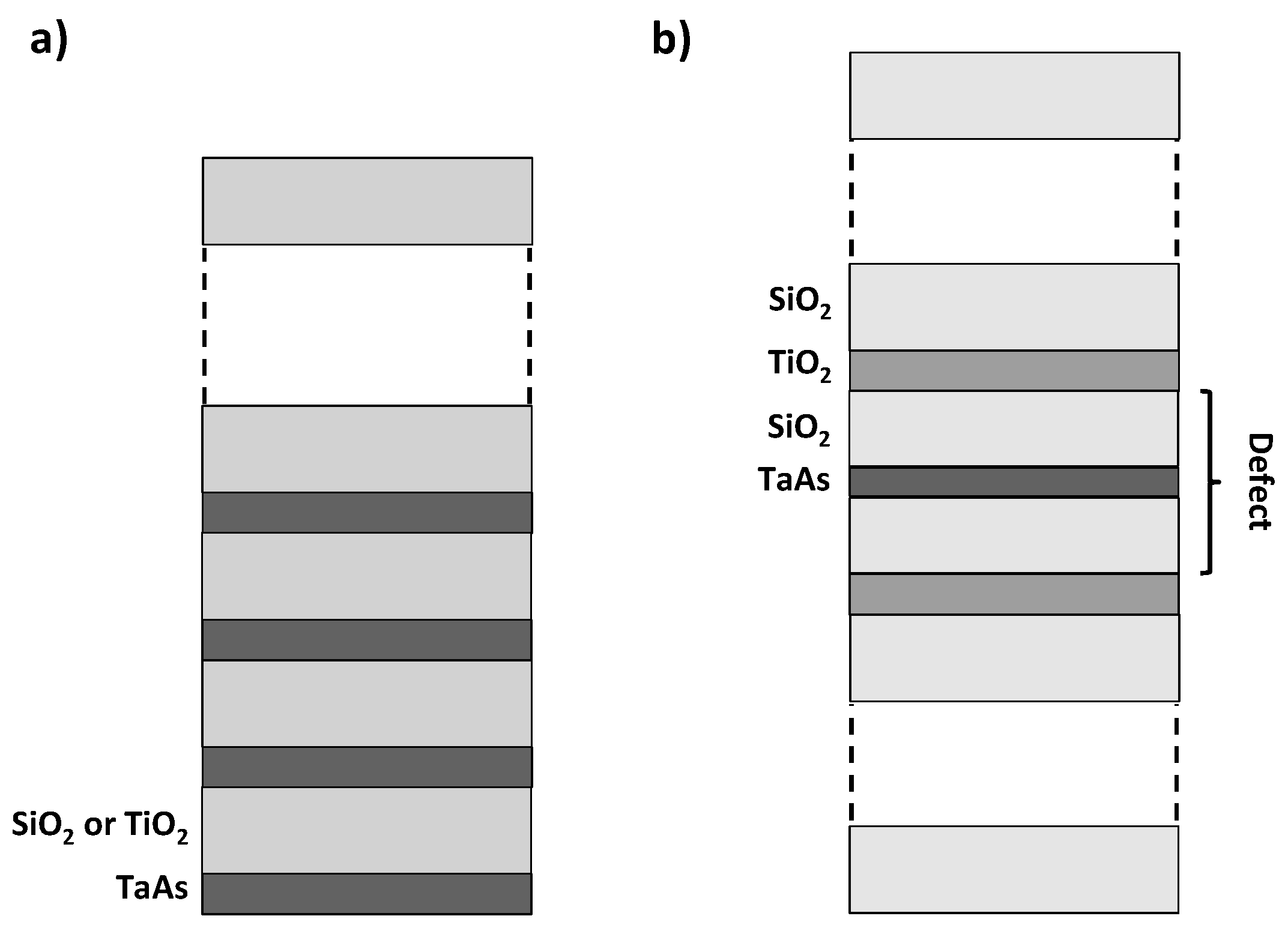
In this work, we studied the optical properties of 1-D photonic crystals made with TaAs alternated with SiO2 or TiO2 and of a microcavity in which TaAs was embedded between two SiO2-TiO2 Bragg mirrors (seven bilayers), as sketched in Figure 1.
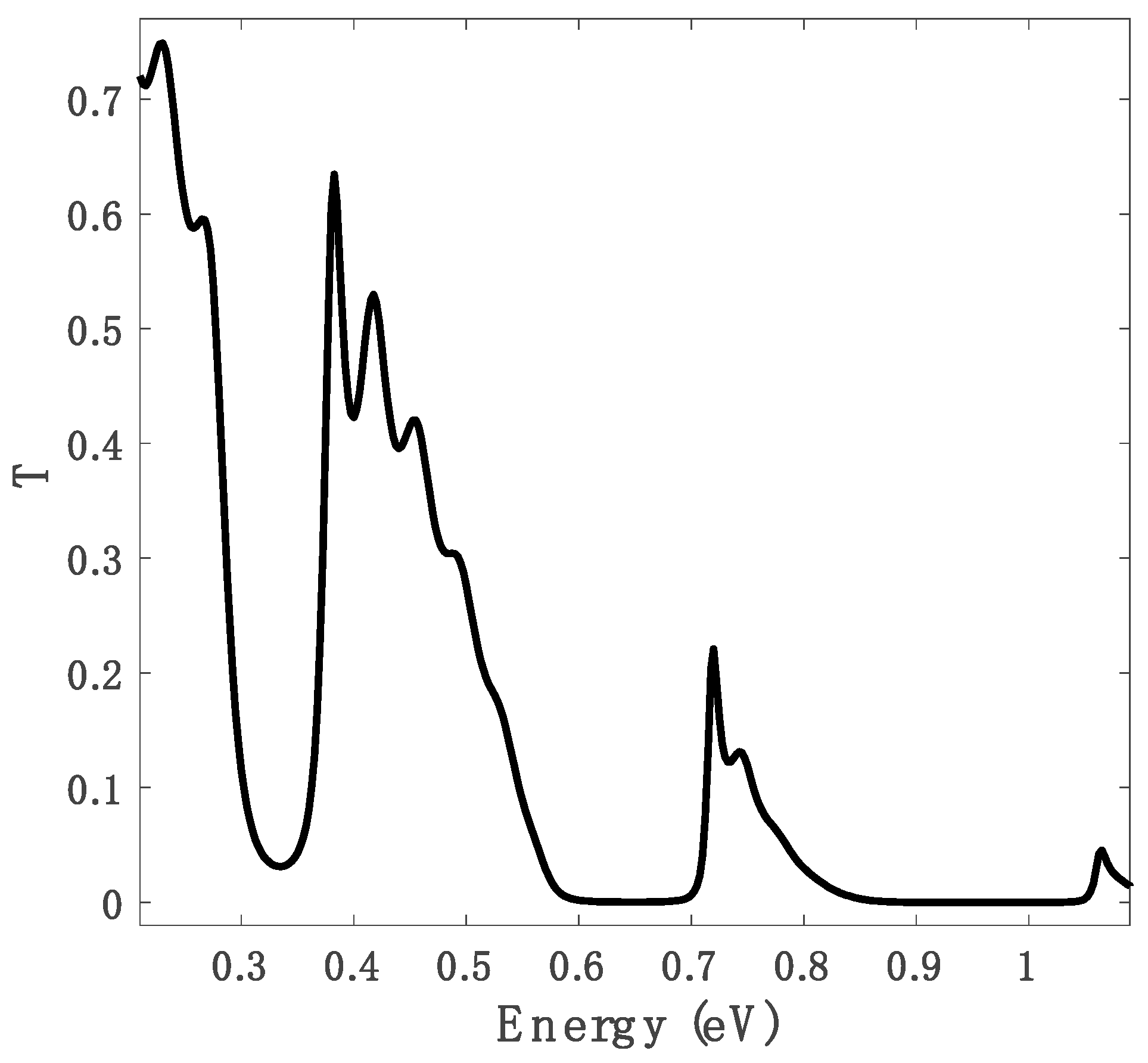
In Figure 2, we show the light transmission spectrum of a photonic crystal made of seven bilayers of TaAs and SiO2. The thickness of each TaAs layer was 16 nm, while the thickness of each SiO2 layer was 1200 nm. n and k (real part and imaginary part of the refractive index) of TaAs, in the c direction of the crystal, have been taken from Reference [9]. The Sellmeier equation for the dispersion of the refractive index of silica is [28]:
The Sellmeier equation for the dispersion of the refractive index of titania, reliable for thin films in the range 0.2–1.1 eV, fits the data by Siefke et al. [29,30] and is
For thicknesses of TaAs above 16 nm, the light absorption of the material became very strong because of the high imaginary part of the refractive index.
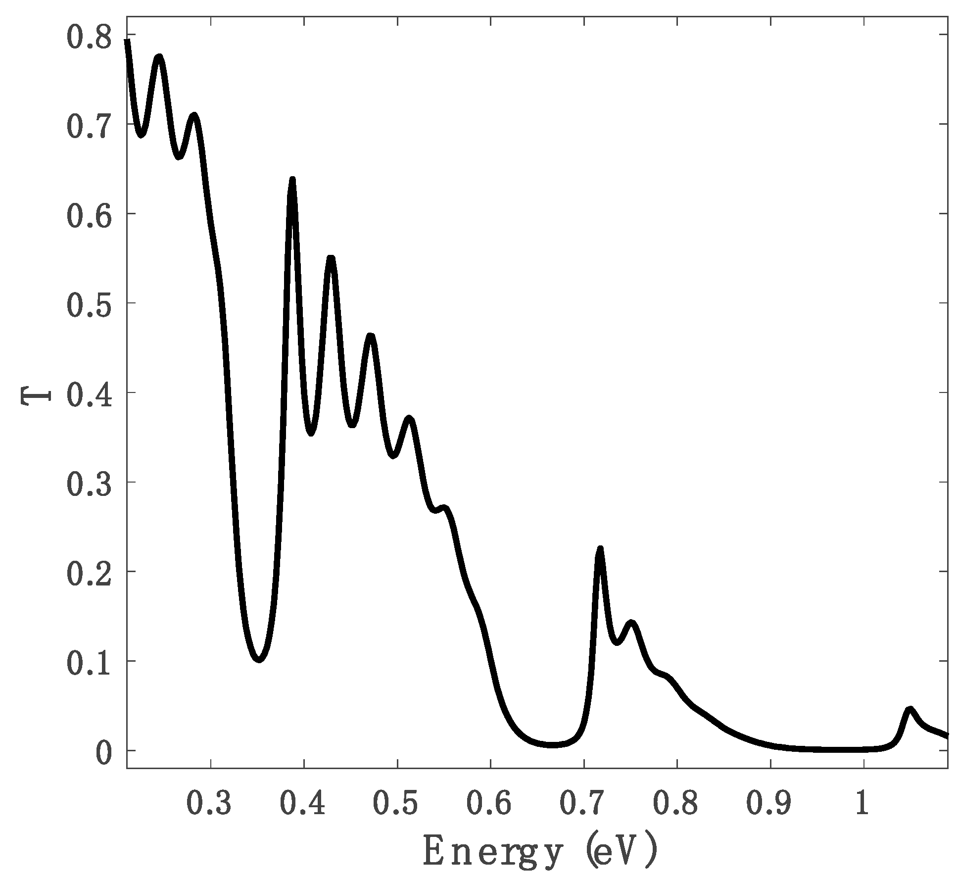
If we used TiO2 instead of SiO2 to be alternated with TaAs, we observed a photonic band gap in the same spectral position (i.e., 0.35 eV) with a thickness of the TiO2 layers of 765 nm, resulting in a thinner photonic crystal. In Figure 3, the light transmission spectrum of a photonic crystal made of TaAs and TiO2 is depicted.
In the spectra in Figure 2 and Figure 3, the transmission valley around 0.65 eV was the second order of the photonic band gap of the photonic crystals. For photon energies above 0.8 eV, the imaginary part of the TaAs complex refractive index increased significantly, such that the transmission valley at 0.9–1.0 eV was mostly due to TaAs absorption [9].
The photonic band gap was less intense with a TaAs-TiO2 unit cell (minimum at about 0.1) with respect to the one with a TaAs-SiO2 unit cell (minimum at about 0.03) because of the smaller refractive index contrast in the TaAs-TiO2 case.
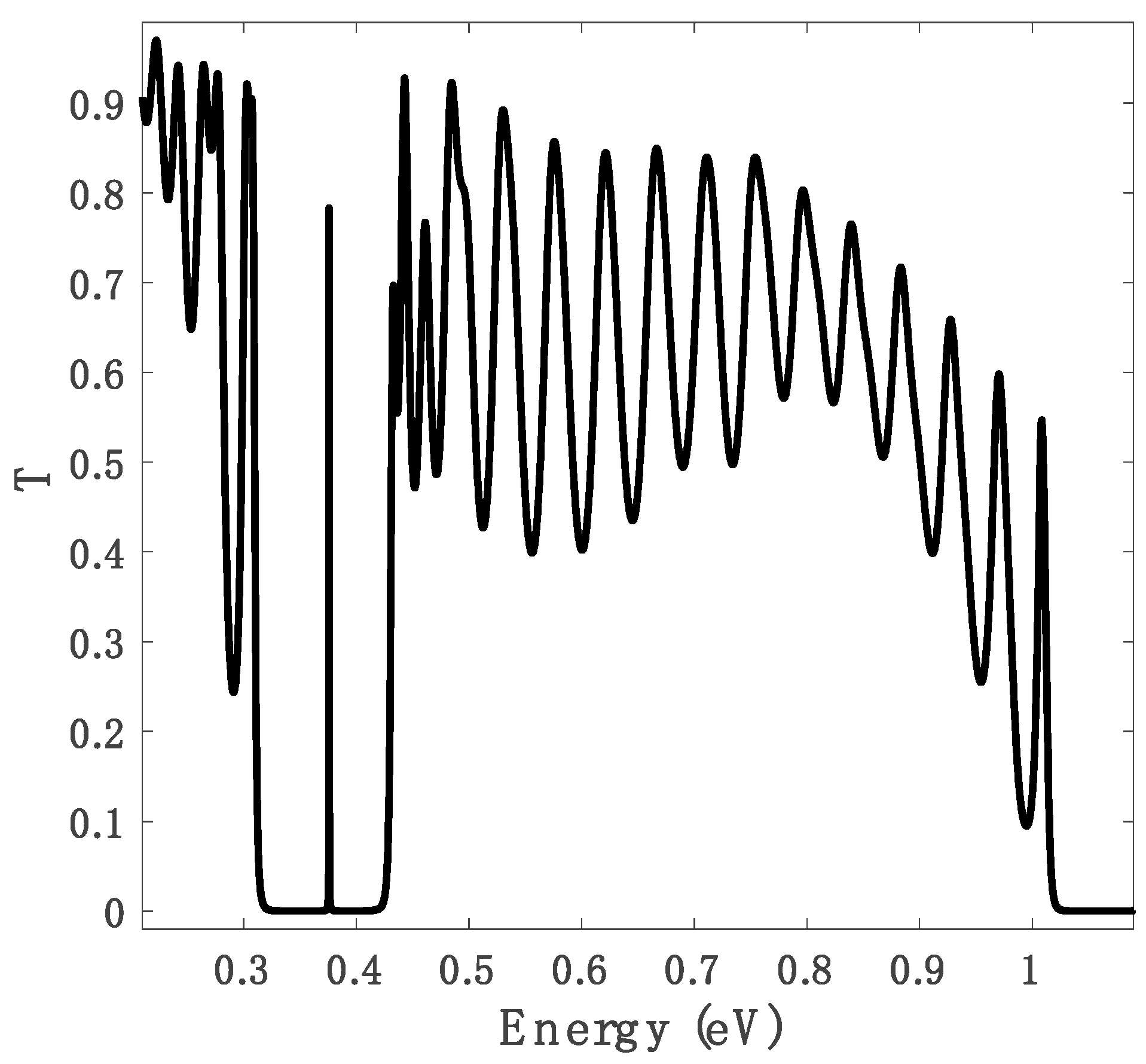
In Figure 4, we show the light transmission spectrum of a (TiO2-SiO2)7-[SiO2-TaAs-SiO2]-(SiO2-TiO2)7 microcavity. The TiO2 layers of the [TiO2-SiO2]7 Bragg mirrors were 377.78 nm thick, while the SiO2 layers were 590.28 nm thick. In this way, the TiO2 layers and SiO2 layers followed the condition nSiO2dSiO2 ≅ nTiO2dTiO2. The two SiO2 layers that sandwiched the TaAs layer in the cavity defect were 560 nm thick, while the thickness of the TaAs layer was 8 nm. The microcavity shows in the region 0.31–0.42 eV a photonic band gap with an intense defect peak at 0.376 eV. Since nSiO2dSiO2 ≅ nTiO2dTiO2, the second order of the microcavity photonic band gap was not observed.
4. Conclusions
In this work, we have exploited the high refractive index of tantalum arsenide in the infrared region (in the region 0.2–1.1 eV), employing the material as a layer in the engineering of a 1-D multilayer photonic crystal and of a 1-D microcavity. We showed one-dimensional photonic crystals alternating TaAs with SiO2 or TiO2 and a microcavity where a layer of TaAs was embedded between two SiO2-TiO2 multilayers. It is worth noting that with thin TaAs layers, 8 to 16 nm thick, it is possible to build photonic crystals and microcavities in the infrared region with good efficiency. This can be promising for the fabrication of thin filters for this spectral region.
Author Contributions
I.K. and M.G. contributed with scientific discussions and the writing of paper. F.S. performed the calculations and guided the project.
Funding
This project has received funding from the European Union’s Horizon 2020 research and innovation program (MOPTOPus) under the Marie Skłodowska-Curie grant agreement No. [705444], as well as (SONAR) grant agreement No. [734690].
Conflicts of Interest
The authors declare no conflict of interest.
References
- Yan, B.; Felser, C. Topological Materials: Weyl Semimetals. Annu. Rev. Condens. Matter Phys. 2017, 8, 337–354. [Google Scholar] [CrossRef] [Green Version]
- Xu, S.-Y.; Belopolski, I.; Alidoust, N.; Neupane, M.; Bian, G.; Zhang, C.; Sankar, R.; Chang, G.; Yuan, Z.; Lee, C.-C.; et al. Discovery of a Weyl fermion semimetal and topological Fermi arcs. Science 2015, 349, 613–617. [Google Scholar] [CrossRef] [PubMed] [Green Version]
- Yang, L.X.; Liu, Z.K.; Sun, Y.; Peng, H.; Yang, H.F.; Zhang, T.; Zhou, B.; Zhang, Y.; Guo, Y.F.; Rahn, M.; et al. Weyl semimetal phase in the non-centrosymmetric compound TaAs. Nat. Phys. 2015, 11, 728–732. [Google Scholar] [CrossRef] [Green Version]
- Lv, B.Q.; Weng, H.M.; Fu, B.B.; Wang, X.P.; Miao, H.; Ma, J.; Richard, P.; Huang, X.C.; Zhao, L.X.; Chen, G.F.; et al. Experimental Discovery of Weyl Semimetal TaAs. Phys. Rev. X 2015, 5. [Google Scholar] [CrossRef]
- Lv, B.Q.; Xu, N.; Weng, H.M.; Ma, J.Z.; Richard, P.; Huang, X.C.; Zhao, L.X.; Chen, G.F.; Matt, C.E.; Bisti, F.; et al. Observation of Weyl nodes in TaAs. Nat. Phys. 2015, 11, 724–727. [Google Scholar] [CrossRef] [Green Version]
- Lv, B.Q.; Muff, S.; Qian, T.; Song, Z.D.; Nie, S.M.; Xu, N.; Richard, P.; Matt, C.E.; Plumb, N.C.; Zhao, L.X.; et al. Observation of Fermi-Arc Spin Texture in TaAs. Phys. Rev. Lett. 2015, 115. [Google Scholar] [CrossRef] [PubMed]
- Wu, L.; Patankar, S.; Morimoto, T.; Nair, N.L.; Thewalt, E.; Little, A.; Analytis, J.G.; Moore, J.E.; Orenstein, J. Giant anisotropic nonlinear optical response in transition metal monopnictide Weyl semimetals. Nat. Phys. 2017, 13, 350–355. [Google Scholar] [CrossRef]
- Weber, C.P.; Berggren, B.S.; Masten, M.G.; Ogloza, T.C.; Deckoff-Jones, S.; Madéo, J.; Man, M.K.L.; Dani, K.M.; Zhao, L.; Chen, G.; et al. Similar ultrafast dynamics of several dissimilar Dirac and Weyl semimetals. J. Appl. Phys. 2017, 122, 223102. [Google Scholar] [CrossRef] [Green Version]
- Buckeridge, J.; Jevdokimovs, D.; Catlow, C.R.A.; Sokol, A.A. Bulk electronic, elastic, structural, and dielectric properties of the Weyl semimetal TaAs. Phys. Rev. B 2016, 93. [Google Scholar] [CrossRef] [Green Version]
- Sakoda, K. Optical Properties of Photonic Crystals; Springer Science & Business Media: Berlin, Germany, 2004; ISBN 978-3-540-20682-8. [Google Scholar]
- Joannopoulos, J.D. Photonic Crystals: Molding the Flow of Light; Princeton University Press: Princeton, NJ, USA, 2008; ISBN 978-0-691-12456-8. [Google Scholar]
- Yablonovitch, E. Inhibited Spontaneous Emission in Solid-State Physics and Electronics. Phys. Rev. Lett. 1987, 58, 2059–2062. [Google Scholar] [CrossRef] [PubMed]
- John, S. Strong localization of photons in certain disordered dielectric superlattices. Phys. Rev. Lett. 1987, 58, 2486–2489. [Google Scholar] [CrossRef] [PubMed]
- Bonifacio, L.D.; Lotsch, B.V.; Puzzo, D.P.; Scotognella, F.; Ozin, G.A. Stacking the Nanochemistry Deck: Structural and Compositional Diversity in One-Dimensional Photonic Crystals. Adv. Mater. 2009, 21, 1641–1646. [Google Scholar] [CrossRef]
- Scotognella, F.; Puzzo, D.P.; Zavelani-Rossi, M.; Clark, J.; Sebastian, M.; Ozin, G.A.; Lanzani, G. Two-Photon Poly(phenylenevinylene) DFB Laser. Chem. Mater. 2011, 23, 805–809. [Google Scholar] [CrossRef]
- Von Freymann, G.; Kitaev, V.; Lotsch, B.V.; Ozin, G.A. Bottom-up assembly of photonic crystals. Chem. Soc. Rev. 2013, 42, 2528–2554. [Google Scholar] [CrossRef] [PubMed] [Green Version]
- Chiasera, A.; Scotognella, F.; Criante, L.; Varas, S.; Valle, G.D.; Ramponi, R.; Ferrari, M. Disorder in Photonic Structures Induced by Random Layer Thickness. Sci. Adv. Mater. 2015, 7, 1207–1212. [Google Scholar] [CrossRef]
- Bellingeri, M.; Chiasera, A.; Kriegel, I.; Scotognella, F. Optical properties of periodic, quasi-periodic, and disordered one-dimensional photonic structures. Opt. Mater. 2017, 72, 403–421. [Google Scholar] [CrossRef] [Green Version]
- Manfredi, G.; Lova, P.; Di Stasio, F.; Rastogi, P.; Krahne, R.; Comoretto, D. Lasing from dot-in-rod nanocrystals in planar polymer microcavities. RSC Adv. 2018, 8, 13026–13033. [Google Scholar] [CrossRef] [Green Version]
- Criante, L.; Scotognella, F. Low-Voltage Tuning in a Nanoparticle/Liquid Crystal Photonic Structure. J. Phys. Chem. C 2012, 116, 21572–21576. [Google Scholar] [CrossRef]
- Lova, P.; Grande, V.; Manfredi, G.; Patrini, M.; Herbst, S.; Würthner, F.; Comoretto, D. All-Polymer Photonic Microcavities Doped with Perylene Bisimide J-Aggregates. Adv. Opt. Mater. 2017, 5, 1700523. [Google Scholar] [CrossRef]
- Lova, P.; Cortecchia, D.; Krishnamoorthy, H.N.S.; Giusto, P.; Bastianini, C.; Bruno, A.; Comoretto, D.; Soci, C. Engineering the Emission of Broadband 2D Perovskites by Polymer Distributed Bragg Reflectors. ACS Photonics 2018, 5, 867–874. [Google Scholar] [CrossRef]
- Park, C.; Yoon, J.; Thomas, E.L. Enabling nanotechnology with self assembled block copolymer patterns. Polymer 2003, 44, 6725–6760. [Google Scholar] [CrossRef]
- Szendrei, K.; Jiménez-Solano, A.; Lozano, G.; Lotsch, B.V.; Míguez, H. Fluorescent Humidity Sensors Based on Photonic Resonators. Adv. Opt. Mater. 2017, 5, 1700663. [Google Scholar] [CrossRef]
- Giusto, P.; Lova, P.; Manfredi, G.; Gazzo, S.; Srinivasan, P.; Radice, S.; Comoretto, D. Colorimetric Detection of Perfluorinated Compounds by All-Polymer Photonic Transducers. ACS Omega 2018, 3, 7517–7522. [Google Scholar] [CrossRef]
- Born, M.; Wolf, E. Principles of Optics: Electromagnetic Theory of Propagation, Interference and Diffraction of Light; Cambridge University Press: Cambridge, UK, 2000; ISBN 978-0-521-78449-8. [Google Scholar]
- Xiao, X.; Wenjun, W.; Shuhong, L.; Wanquan, Z.; Dong, Z.; Qianqian, D.; Xuexi, G.; Bingyuan, Z. Investigation of defect modes with Al2O3 and TiO2 in one-dimensional photonic crystals. Opt. Int. J. Light Electron Opt. 2016, 127, 135–138. [Google Scholar] [CrossRef]
- Malitson, I.H. Interspecimen Comparison of the Refractive Index of Fused Silica. J. Opt. Soc. Am. 1965, 55, 1205–1208. [Google Scholar] [CrossRef]
- Siefke, T.; Kroker, S.; Pfeiffer, K.; Puffky, O.; Dietrich, K.; Franta, D.; Ohlídal, I.; Szeghalmi, A.; Kley, E.-B.; Tünnermann, A. Materials Pushing the Application Limits of Wire Grid Polarizers further into the Deep Ultraviolet Spectral Range. Adv. Opt. Mater. 2016, 4, 1780–1786. [Google Scholar] [CrossRef] [Green Version]
- Polyanskiy, M.N. Refractive Index Database. Available online: http://refractiveindex.info (accessed on 11 August 2018).
Figure 1.
Scheme of (a) a TaAs/SiO2 (or TaAs/TiO2) photonic crystal and of (b) a (TiO2-SiO2)7-[SiO2-TaAs-SiO2]-(SiO2-TiO2)7 microcavity.
Figure 1.
Scheme of (a) a TaAs/SiO2 (or TaAs/TiO2) photonic crystal and of (b) a (TiO2-SiO2)7-[SiO2-TaAs-SiO2]-(SiO2-TiO2)7 microcavity.

Figure 2.
Light transmission spectrum of a 1-D photonic crystal made using seven bilayers of TaAs and SiO2.
Figure 2.
Light transmission spectrum of a 1-D photonic crystal made using seven bilayers of TaAs and SiO2.

Figure 3.
Light transmission spectrum of a 1-D photonic crystal made using seven bilayers of TaAs and TiO2.
Figure 3.
Light transmission spectrum of a 1-D photonic crystal made using seven bilayers of TaAs and TiO2.

Figure 4.
Light transmission spectrum of a (TiO2-SiO2)7-[SiO2-TaAs-SiO2]-(SiO2-TiO2)7 microcavity.

© 2018 by the authors. Licensee MDPI, Basel, Switzerland. This article is an open access article distributed under the terms and conditions of the Creative Commons Attribution (CC BY) license (http://creativecommons.org/licenses/by/4.0/).
Share and Cite
MDPI and ACS Style
Kriegel, I.; Guizzardi, M.; Scotognella, F. Tantalum Arsenide-Based One-Dimensional Photonic Structures. Ceramics 2018, 1, 139-144. https://doi.org/10.3390/ceramics1010012
AMA Style
Kriegel I, Guizzardi M, Scotognella F. Tantalum Arsenide-Based One-Dimensional Photonic Structures. Ceramics. 2018; 1(1):139-144. https://doi.org/10.3390/ceramics1010012
Chicago/Turabian StyleKriegel, Ilka, Michele Guizzardi, and Francesco Scotognella. 2018. "Tantalum Arsenide-Based One-Dimensional Photonic Structures" Ceramics 1, no. 1: 139-144. https://doi.org/10.3390/ceramics1010012