Article

Electrical Behavior and Microstructural Features of Electric Field-Assisted and Conventionally Sintered 3 mol% Yttria-Stabilized Zirconia

by
Sabrina G.M. Carvalho
1,*,
Eliana N.S. Muccillo
1 and
Reginaldo Muccillo
1,2
1
Energy and Nuclear Research Institute, S. Paulo, SP, 05508-900, Brazil
2
Center of Engineering, Modeling and Applied Social Sciences, Federal University of ABC, Santo André, SP, 09210-580, Brazil
*
Author to whom correspondence should be addressed.
Ceramics 2018, 1(1), 3-12; https://doi.org/10.3390/ceramics1010002
Submission received: 28 December 2017 / Revised: 10 February 2018 / Accepted: 18 February 2018 / Published: 21 February 2018
(This article belongs to the Special Issue Novel Processing Routes of Ceramics for Functional Applications)

Abstract

:
ZrO2: 3 mol% Y2O3 (3YSZ) polycrystalline pellets were sintered at 1400 °C and by applying an alternating current (AC) electric field at 1000 °C. An alumina sample holder with platinum wires for connecting the sample to a power supply was designed for the electric field-assisted sintering experiments. The apparent density was evaluated with the Archimedes technique, the grain size distribution by analysis of scanning electron microscopy images, and the electrical behavior by the impedance spectroscopy technique. Sintering with the application of AC electric fields to 3YSZ enhances its ionic conductivity. An explanation is proposed, based on the dissolution back to the bulk of chemical species, which are depleted at the grain boundaries, leading to an increase in the oxygen vacancy concentration. For the enhancement of the grain boundary conductivity, an explanation is given based on the diminution of the concentration of depleted chemical species, which migrate to the bulk. This migration leads to a decrease of the potential barrier of the space charge region, known to be responsible for blocking the oxide ions through the intergranular region. Moreover, the heterogeneity of the distribution of the grain sizes is ascribed to the skin effect, the tendency of the AC current density to be largest near the surface, decreasing towards the bulk.

1. Introduction

Flash sintering is an electric field-assisted sintering technique that consists of applying a direct current (DC) or alternating current (AC) electric field to a green or pre-sintered ceramic compact to trigger an electric current through the specimen, usually leading to densification at lower temperatures and shorter times than the ones applied in conventional sintering (a process of grain-growth-induced densification facilitated by atomic diffusion at approximately two-thirds of the melting temperature [1]) [2]. Moreover, grain growth is inhibited in yttria-stabilized zirconia [2,3,4,5]. The electric field can be applied either during heating up to a temperature below the conventional sintering temperature or at a fixed temperature.
The first paper announcing the development of the flash sintering technique was focused on the study of the influence of the electric field on the sintering rate of 3 mol% yttria-stabilized zirconia (3YSZ) [3]; the sample was submitted to a 4 V·cm−1 DC electric field, producing an increase of the sintering rate. It was proposed that the sintering rate increased due to the retardation of the grain growth dynamics as a consequence of the application of the electric field, with acceleration of the densification. Moreover, higher electric fields produced samples with smaller average grain sizes. A comparison of the densification rate using AC and DC electric fields reported that the sintering rate was higher for AC than for DC electric fields [4]; the phenomenon of sintering the 3YSZ ceramic samples under a DC electric field of 120 V·cm−1 at 850 °C was called flash sintering due to the occurrence of the shrinkage in a few seconds [2].
The electric field-assisted pressureless sintering technique has mainly been applied to yttria-stabilized zirconia ceramics [2,3,4,5,6,7,8,9,10,11,12,13,14,15,16]. Many other reports were published applying this technique to other materials [16,17,18,19,20,21,22,23,24,25,26,27,28,29,30], studying the dependence on the amplitudes of the electric field and current density [31], on the average particle size [32], on the porosity [33], and searching for an explanation of such events [34,35,36,37,38,39,40].
Three recent reviews on flash sintering give details of some experimental setups, ceramics submitted to flash sintering, proposed mechanisms, electrical measurements, and modeling [17,18,19].
We describe here the relationship between the microstructure and the electrical properties of 3 mol% yttria-stabilized zirconia specimens, which were sintered according to three different procedures: isothermal flash sintering—applying an AC electric field at a constant temperature; conventional method—heating and cooling; and conventional followed by the isothermal flash event. The bulk and the grain boundary electrical resistivities were found to depend on those procedures, due to the different final microstructures. Moreover, the observation that the average grain size on the surface of the AC flash sintered samples decreases from near the border to the center of the flat surface may be evidence of the classical skin effect, i.e., it depends on the AC current density. The main objective of this work was to study the relationship between the microstructure and the electrical properties of yttria-stabilized zirconia solid electrolytes sintered according to the three procedures described above.

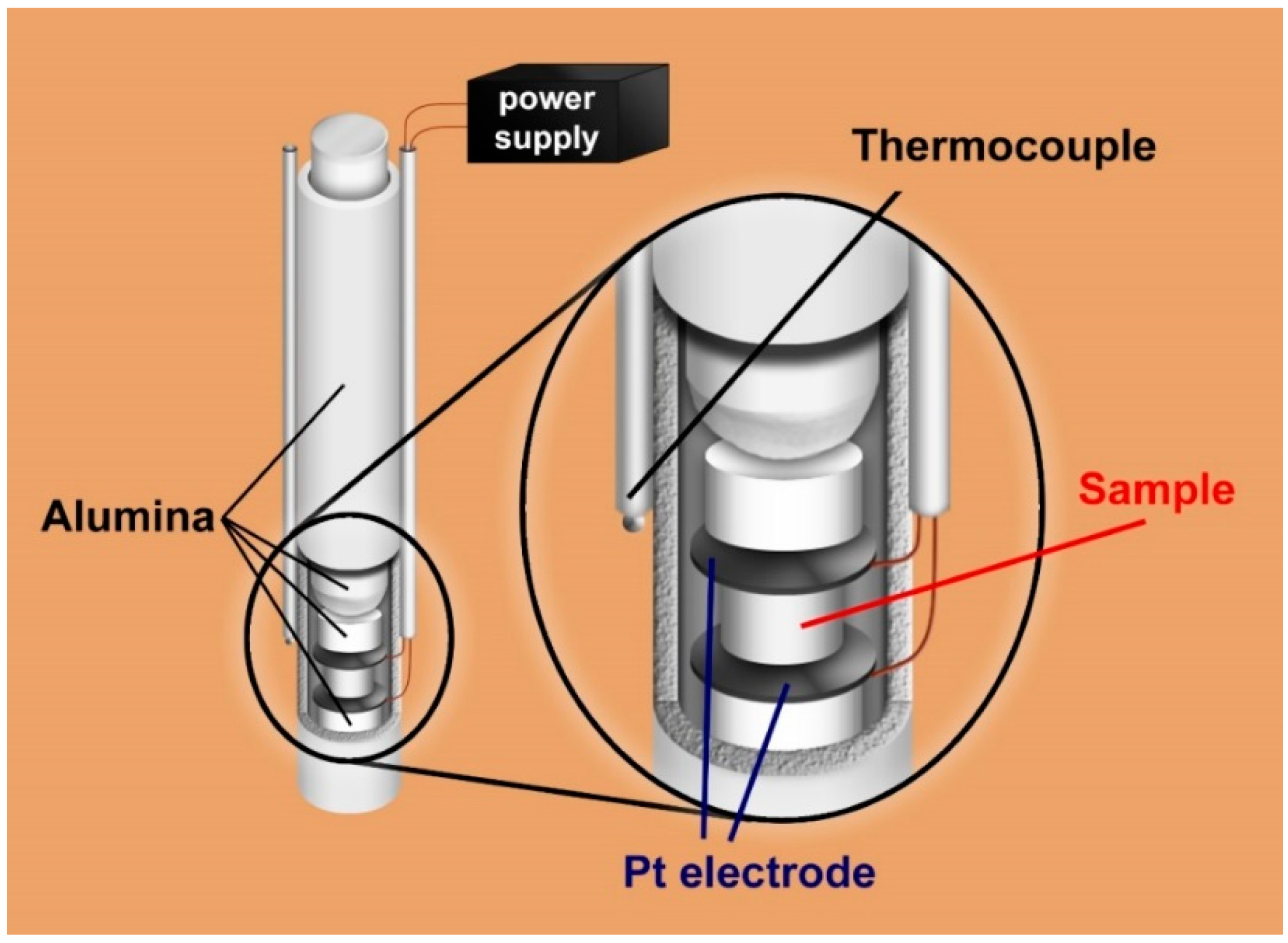
2. Materials and Methods

ZrO2: 3 mol% Y2O3 ceramic powder (Tosoh TZ-3YBE, Tokyo, Japan) was uniaxially cold-pressed (Φ 10 mm × 3 mm) with 50 MPa in a metallic cylindrical die, followed by vacuum sealing for isostatic pressing (National Forge Co., Irvine, CA, USA) with 200 MPa. Green densities were in the 45–50% T.D. (theoretical density) range.
Three experimental procedures were carried out to evaluate the main differences between conventional and flash sintering: (a) heating up a green pellet to 1400 °C at 10 °C·min−1 with no dwell time, and cooling down to room temperature at the same rate (conventional sintering); (b) heating up a green pellet to 1000 °C and applying at that temperature 200 V·cm−1, 1000 Hz for 5 min, limiting the amplitude of the electric current to 3 A (flash sintering); (c) heating a pellet (pre-sintered at 1400 °C) to 1000 °C and applying at that temperature 200 V·cm−1, 1000 Hz for 5 min, limiting the amplitude of the electric current to 3 A (conventional + flash event). During the flash sintering experiment, a voltage is applied in the 0–100 V range until the sample reaches a pre-set electrical current; the power supply switches from voltage to current control, maintaining the pre-set electric current throughout the programmed time.
The sample chamber for flash sintering, shown in Figure 1, consists of a vertical alumina sample holder connected, via alumina-insulated platinum wires, to a commercial power supply (Pacific Power Source 118-ACX, Irvine, CA, USA). The sample was positioned between two platinum thin foils with platinum leads connecting the sample electrodes to the power supply; to ensure electrical contact, a Pt paste was used to cover the parallel faces of the specimen. A chromel-alumel thermocouple with its junction positioned close to the sample was used to monitor the local temperature. The sample chamber was inserted in a programmable furnace that was heated up to a fixed temperature to apply the electric voltage.
Polished (15 µm to 3 µm diamond paste) and thermally etched (1300 °C/15 min) surfaces of the sintered specimens were observed in a scanning electron microscope (Inspect F50 FEG-SEM, FEI, Brno, Czech Republic). The Mendelson method [41] and the Image J software [42] were used for the evaluation of the distribution of grain sizes.
Impedance spectroscopy measurements in sintered specimens were carried out in the 370 °C–450 °C range with a Hewlett Packard 4192A impedance analyzer (Yokogawa-Hewlett Packard, Tokyo, Japan) in the 5 Hz to 13 MHz frequency range with a 200 mV signal amplitude. The impedance spectroscopy data were collected in sintered samples with the parallel surfaces covered with Ag paste and cured at 300 °C for removal of the organic binder; the sample holder had Pt disks and Pt wires for connecting the sample to the impedance analyzer. The [−Z''(f) × Z'(f)] impedance diagrams were deconvoluted in frequency to obtain the intergranular and the intragranular (bulk) electrical resistivities [43].

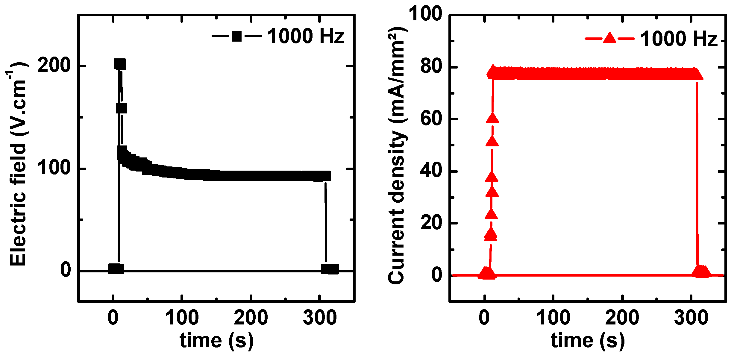
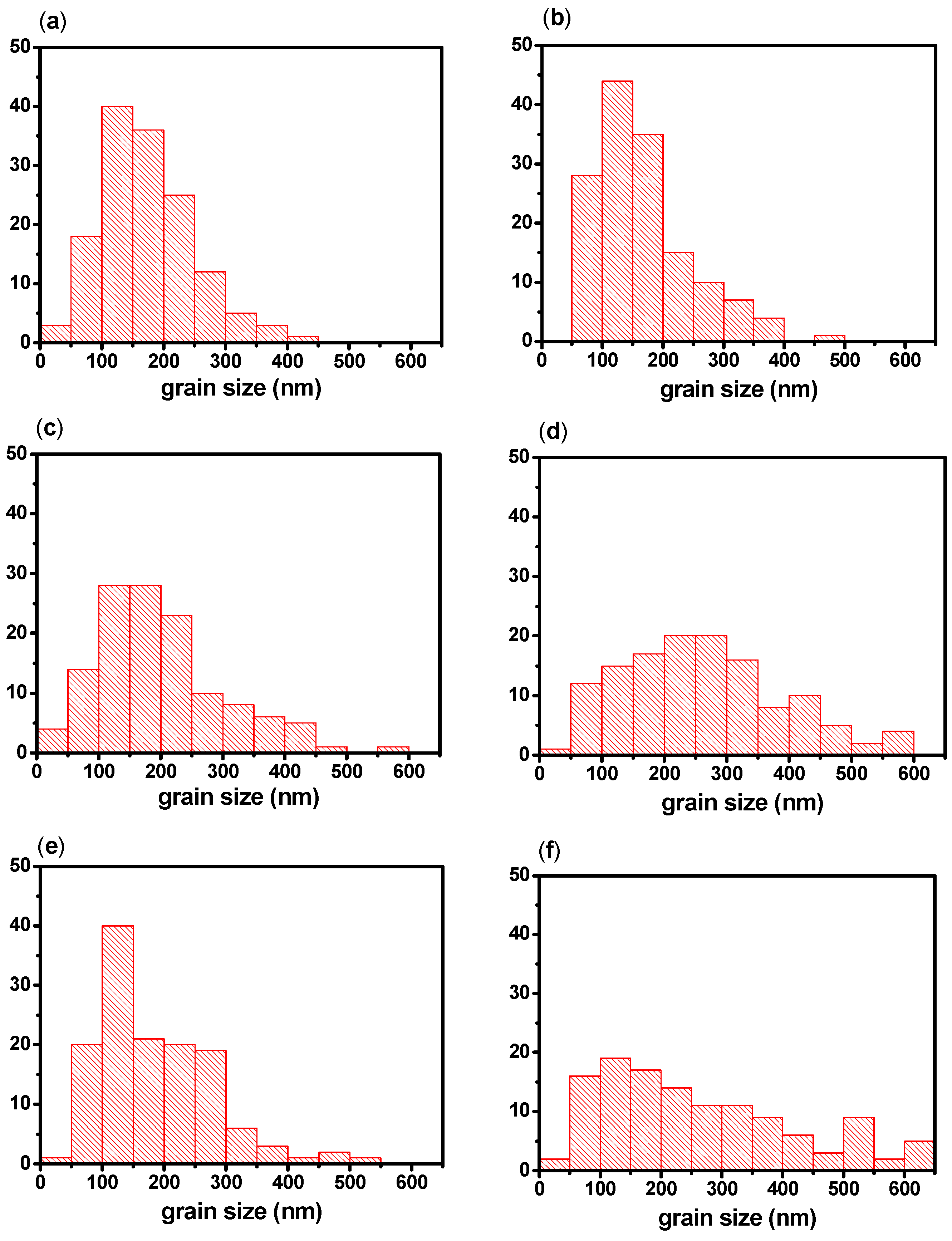
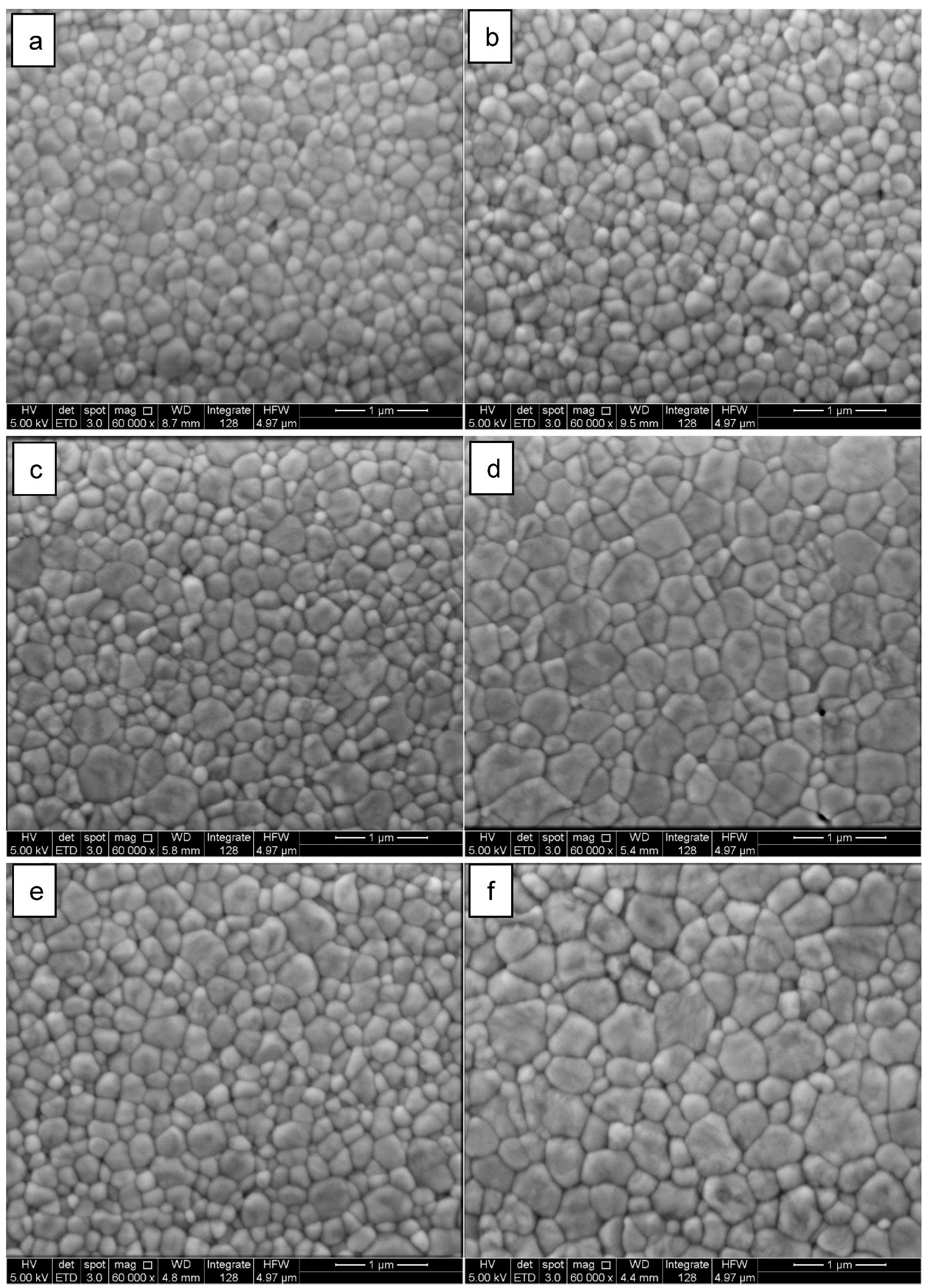
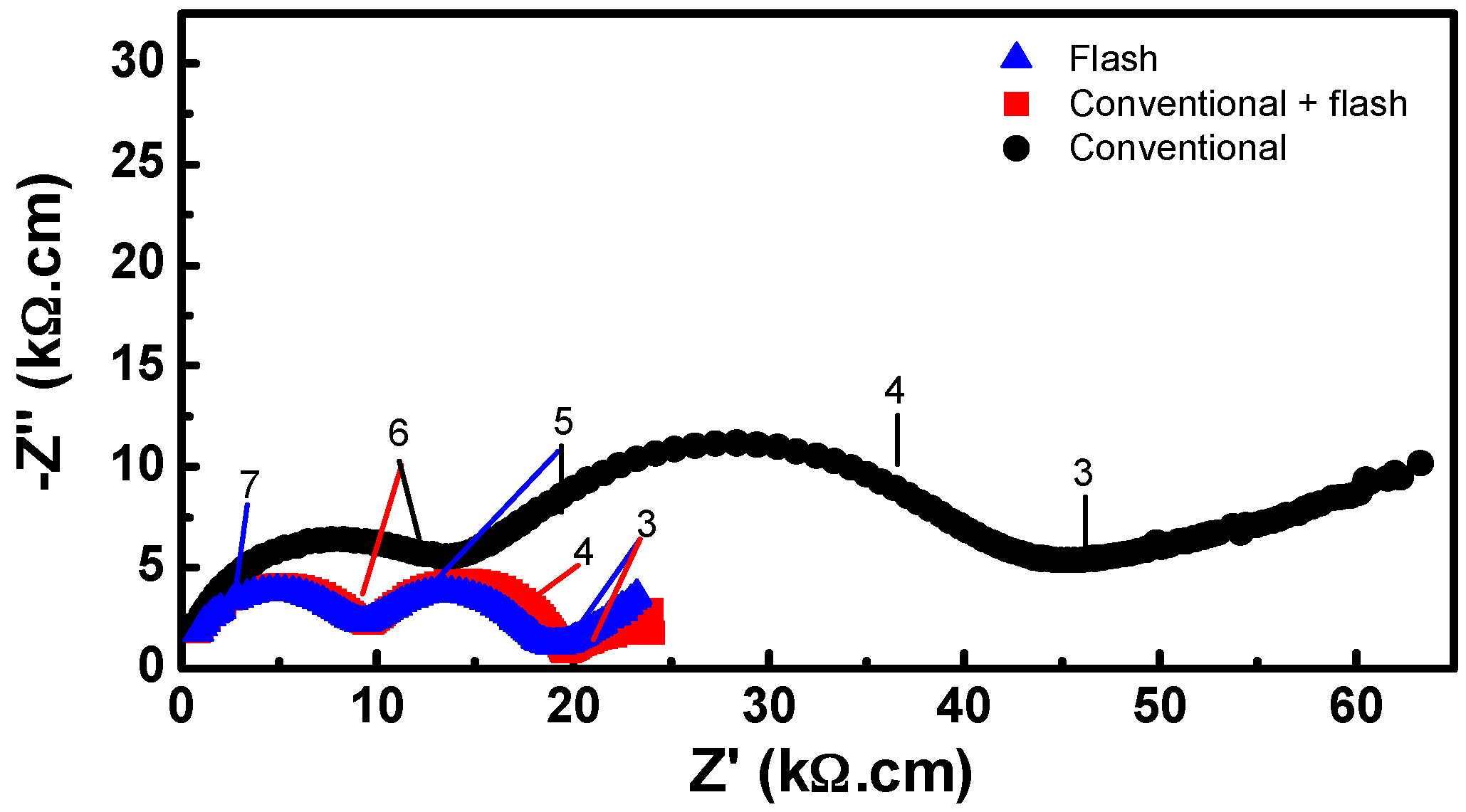
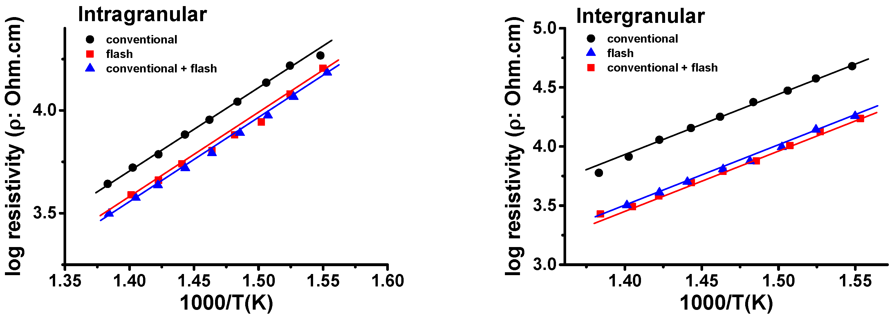
3. Results and Discussion

The apparent density of the 3YSZ samples sintered according to three different processes (conventional, flash, and conventional + flash) was evaluated by the Archimedes method as 98.9(1), 98.6(1), and 99.1(1)% T.D., respectively. This is evidence that the electric current pulse through the sample is able to eliminate residual porosity not only in the flash sintered sample, but also in the dense (conventionally sintered) sample.
Figure 2 shows the electric field and current plotted as a function of time, collected during the flash sintering experiment. As soon as an electric current pulse flows through the sample, the electric field decreases to keep the pre-set current value constant. This procedure is undertaken to avoid electrical runaway that could occur with the increase in current, due to the decrease of the electrical resistance of the sample, caused by the raise of the temperature promoted by Joule heating.
Figure 3 shows FEG-SEM micrographs of surfaces of 3YSZ after conventional sintering at 1400 °C (Figure 3a,b), flash sintering at 1000 °C (Figure 3c,d), and conventional sintering followed by the flash event at 1000 °C (Figure 3e,f). The observations were focused at the center (figures on the left) and near the border (right) of the sample flat cylindrical surfaces. All samples present grains with an average submicron size and low pore density. The conventionally sintered samples are homogeneous with both a similar average grain size and distribution of grain size in the entire surface; the flash sintered samples, on the other hand, have larger grains near the border relative to the center of the flat surfaces, meaning that the Joule heating generated by the electric current pulse is more intense at the border than at the center. This may be caused by the skin effect, i.e., the decrease of the AC electric current from the extreme end of the top surface in the radial direction to the center of that surface [44].
The sample sintered at 1400 °C (Figure 3a,b) without application of the electric field has similar grains at the center and near the border of the flat polished and thermally etched surfaces. The flash sintered sample (Figure 3c,d), on the other hand, shows irregular grain sizes at the center, probably due to the non-homogeneous distribution of the electric current pulse through the specimen. Uniaxially pressed ceramic powders form green pellets that, even after further isostatic pressing, do not have a homogeneous distribution of density and interparticle pores [45]. The application of an electric field at a temperature located in the first stage of sintering results in an electric current pulse after an incubation time. Considering that pores play a role in the electric current pulse event [33], the non-homogeneous pore distribution may lead to different electric current densities and, consequently, to different grain sizes throughout the flash sintered specimen. The evaluation of the grain size distribution gave the following values: specimens sintered at 1400 °C, sintered at 1400 °C followed by the flash event, and flash sintered, have average grain sizes of 282 ± 73, 340 ± 108, and 385 ± 133 nm, respectively. Flash sintering then promotes grain growth in pre-sintered samples. Moreover, flash sintered samples have a larger average grain size than conventionally sintered samples, probably due to the higher availability of preferential paths for the electric current pulse.
The distribution of the grain sizes, evaluated with the SEM micrographs of Figure 3a–f, is shown in Figure 4. The average grain size measured at the center of the surface of the disc-shaped 3YSZ specimens sintered at 1400 °C is similar to the one measured near the border. On the other hand, the same parameter measured in surfaces of 3YSZ specimens sintered with the application of an electric field at 1000 °C are larger near the border than at the center of the surfaces. This means that the Joule heating is more effective near the border, i.e., the electric current density is larger in that region. This could be due to the skin effect, which states that the current density depends on the frequency of the AC electric field, decreasing from the border to the center [44].
Figure 5 shows the impedance diagrams of 3YSZ sintered at 1400 °C, flash sintered, and flash sintered specimens previously sintered at 1400 °C. All diagrams consist of two semicircles, one at high frequencies corresponding to the electrical response of the bulk, and the other at low frequencies, corresponding to the intergranular contribution (interfaces, usually grain boundaries and pores). The total electrical resistivity of the 3YSZ sintered at 1400 °C is 45 kΩ·cm, higher than the value determined for the sintered sample submitted to the flash event. There is a decrease of the intergranular resistivity (low frequency region) and also of the bulk resistivity (high frequency region). It has been reported that the space charge region in yttria-stabilized zirconia consists of a positively charged nucleus with an excess of oxygen vacancy and an accumulation of yttrium, for the electroneutrality (charge compensation) [46,47]. The decrease of the intergranular resistivity is attributed to the welding of the grains [6,8] and the decrease of the intragranular resistivity to the increase in the oxide ion concentration due to the thermal migration to the bulk of the chemical species depleted at the space charge region, enhancing the oxide ion concentration, and consequently the ionic conductivity. Both phenomena are primarily a consequence of the Joule heating produced by the electric current pulse.
There is a large difference between the electrical resistivity value of the sample submitted to conventional sintering comparing and the two other situations. The deconvolution of these diagrams allowed for evaluating the intergranular and the intragranular components of the total resistivity. Figure 6 shows the Arrhenius plots of the intragranular and the intergranular electrical resistivities of the sintered samples.
The conventionally sintered sample has a higher intergranular electric resistivity than samples submitted to flash sintering. The samples sintered with application of the electric field are less resistive (see Figure 5) under the same measuring conditions.
The intragranular values do not differ considerably, as observed in the Arrhenius plots, meaning that flash sintering produces samples with a similar bulk resistivity as samples sintered without applying an electric field. Since the average grain size and density are similar for all samples, the major difference is in the intergranular region: samples submitted to flash sintering present a significant increase of the intergranular conductivity.
The values of the activation energy for the ionic conductivity of the bulk and grain boundary were evaluated and are shown in Table 1. For the grain boundary conductivity of the conventionally sintered sample, it is in agreement with reported values (e.g, 1.09 eV [48]), but it is lower for samples sintered under the electric field. This may be a consequence of the interaction of the electric current pulse, modifying the space charge region with a decrease of the potential of the space charge layer [19]. It has been already reported that the activation energy for the grain boundary resistivity is determined by the properties of the space charge layer [48].

4. Conclusions

Green, as well as conventionally sintered (1400 °C), pellets of ZrO2: 3 mol% Y2O3 solid electrolytes exposed to an AC electric field (flash sintering) at 1000 °C have similar intergranular (grain boundary) and intragranular (bulk) oxide ion conductivities. These conductivities are higher than in conventionally sintered pellets. We propose that the electric current pulse due to the application of the electric field delivers Joule heat to the grain boundary region, promoting thermal migration to the grains of the chemical species located at the interfaces (increasing the oxygen vacancy concentration and consequently the bulk oxide ion conductivity), as well as the welding of the grains (decreasing the potential barrier that blocks the flow of oxide ions and, consequently, increasing the grain boundary conductivity). Moreover, as the grain sizes are larger near the border than at the center of the flash sintered specimens, probably due to the different current densities, we propose that the skin effect may play a role during the flash sintering event with an AC electric field. A larger current density means larger delivered Joule heating, increasing the grain sizes, as we observed in the scanning electron microscopy images.

Acknowledgments

To CNEN, CNPq (Procs. 470952/2013-0 and 303483/2013-0), and FAPESP (CEPID-CDMF, Proc. 2013/07296-2) for financial support. To CAPES for the scholarship to one of the authors (S.G.M. Carvalho).

Author Contributions

Reginaldo Muccillo and Eliana N.S. Muccillo conceived and designed the experiments; Sabrina G.M. Carvalho performed the experiments; Reginaldo Muccillo, Eliana N.S. Muccillo, and Sabrina G.M. Carvalho analyzed the data; Reginaldo Muccillo, Eliana N.S. Muccillo, and Sabrina G.M. Carvalho wrote the paper.

Conflicts of Interest

The authors declare no conflict of interest." “The founding sponsors had no role in the design of the study; in the collection, analyses, or interpretation of data; in the writing of the manuscript, and in the decision to publish the results.

References

  1. Kocjan, A.; Logar, S.M.; Shen, Z. The agglomeration, coalescence and sliding of nanoparticles, leading to the rapid sintering of zirconia nanoceramics. Sci. Rep. 2017, 7, 2541–2548. [Google Scholar] [CrossRef] [PubMed]
  2. Cologna, M.; Rashkova, B.; Raj, R. Flash sintering of nanograin zirconia in < 5 s at 850 °C. J. Am. Ceram. Soc. 2010, 93, 3556–3559. [Google Scholar] [CrossRef]
  3. Gosh, S.; Chokshi, A.H.; Lee, P.; Raj, R. A huge effect of week dc electrical fields on grain growth in zirconia. J. Am. Ceram. Soc. 2009, 92, 1856–1859. [Google Scholar] [CrossRef]
  4. Yang, D.; Conrad, H. Enhanced sintering rate of zirconia (3Y-TZP) by application of a small AC electric field. Scr. Mater. 2010, 63, 328–331. [Google Scholar] [CrossRef]
  5. Yang, D.; Raj, R.; Conrad, H. Enhanced sintering rate of zirconia (3Y-TZP) through the effect of a weak dc electric field on grain growth. J. Am. Ceram. Soc. 2010, 93, 2935–2937. [Google Scholar] [CrossRef]
  6. Cologna, M.; Prette, A.L.G.; Raj, R. Flash-Sintering of cubic yttria-stabilized zirconia at 750 °C for possible use in SOFC manufacturing. J. Am. Ceram. Soc. 2011, 94, 316–319. [Google Scholar] [CrossRef]
  7. Muccillo, R.; de Florio, D.Z.; Fonseca, F.C.; Muccillo, E.N.S. Electric field-assisted co-sintering of planar anode-supported solid oxide fuel cell. In Proceedings of the MRS Fall Meeting, Boston, MA, USA, November 30–December 5, 2014. [Google Scholar]
  8. Muccillo, R.; Kleitz, M.; Muccillo, E.N.S. Flash grain welding in yttria stabilized zirconia. J. Eur. Ceram. Soc. 2012, 31, 1517–1521. [Google Scholar] [CrossRef]
  9. Muccillo, R.; Muccillo, E.N.S. An experimental setup for shrinkage evaluation during electric field-assisted flash sintering: application to yttria-stabilized zirconia. J. Eur. Ceram. Soc. 2013, 33, 515–520. [Google Scholar] [CrossRef]
  10. Downs, J.A.; Sglavo, V.M. Electric field assisted sintering of cubic zirconia at 390 °C. J. Am. Ceram. Soc. 2014, 96, 1342–1344. [Google Scholar] [CrossRef]
  11. Steil, M.C.; Marinha, D.; Aman, Y.; Gomes, J.R.C.; Kleitz, M. From conventional ac flash sintering of YSZ to hyper-flash and double flash. J. Eur. Ceram. Soc. 2013, 33, 2093–2101. [Google Scholar] [CrossRef]
  12. Muccillo, R.; Muccillo, E.N.S. Shrinkage control of yttria-stabilized zirconia during ac electric field-assisted sintering. J. Eur. Ceram. Soc. 2014, 34, 3871–3877. [Google Scholar] [CrossRef]
  13. Muccillo, R.; Muccillo, E.N.S. Light emission during electric field-assisted sintering of electroceramics. J. Eur. Ceram. Soc. 2014, 35, 1653–1656. [Google Scholar] [CrossRef]
  14. da Silva, J.G.P.; Lebrun, J.-M.; Al-Qureshi, H.A.; Janssen, R.; Raj, R. Temperature distributions during flash sintering of 8% yttria-stabilized zirconia. J. Am. Ceram. Soc. 2015, 98, 3525–3528. [Google Scholar] [CrossRef]
  15. Du, Y.X.; Stevenson, A.J.; Vernat, D.; Diaz, M.; Marinha, D. Estimating Joule heating and ionic conductivity during flash sintering of 8YSZ. J. Eur. Ceram. Soc. 2016, 36, 749–759. [Google Scholar] [CrossRef]
  16. Naik, K.S.; Sglavo, V.M.; Raj, R. Field assisted sintering of ceramic constituted by alumina and yttria stabilized zirconia. J. Eur. Ceram. Soc. 2014, 34, 2435–2442. [Google Scholar] [CrossRef]
  17. Dancer, C.E.J. Flash sintering of ceramic materials. Mater. Res. Express 2016, 3, 102001. [Google Scholar] [CrossRef]
  18. Yu, M.; Grasso, S.; McKinnon, R.; Saunders, T.; Reece, M.J. Review of flash sintering: materials, mechanisms and modelling. Adv. Appl. Ceram. 2016, 116, 24–60. [Google Scholar] [CrossRef]
  19. Muccillo, R.; Muccillo, E.N.S. Electric field assisted sintering of electroceramics and in situ analysis by impedance spectroscopy. J. Electroceramics 2016, 38, 24–42. [Google Scholar] [CrossRef]
  20. Luo, J. Scientific questions and technological opportunities of flash sintering: from a case study of ZnO to other ceramics. Scr. Mater. 2018, 146, 260–266. [Google Scholar] [CrossRef]
  21. Prette, A.L.G.; Cologna, M.; Sglavo, V.; Raj, R. Flash-sintering of Co2MnO4 spinel for solid oxide fuel cell applications. J. Power Sources 2011, 196, 2061–2065. [Google Scholar] [CrossRef]
  22. Zapata-Solvas, E.; Bonilla, S.; Wilshaw, P.R.; Todd, R.I. Preliminary investigation of flash sintering of SiC. J. Eur. Ceram. Soc. 2013, 33, 2811–2816. [Google Scholar] [CrossRef]
  23. Gaur, A.; Sglavo, V.M. Flash-sintering of MnCo2O4 and its relation to phase stability. J. Eur. Ceram. Soc. 2014, 34, 2391–2400. [Google Scholar] [CrossRef]
  24. M’Peko, J.-C.; Francis, J.S.C.; Raj, R. Field-assisted sintering of undoped BaTiO3: Microstructure evolution and dielectric permittivity. J. Eur. Ceram. Soc. 2014, 34, 3655–3660. [Google Scholar] [CrossRef]
  25. Gaur, A.; Sglavo, V.M. Flash Sintering of (La, Sr)(Co, Fe)O3-Gd-Doped CeO2 Composite. J. Am. Ceram. Soc. 2015, 98, 1747–1752. [Google Scholar] [CrossRef]
  26. Biesuz, M.; Sglavo, V.M. Flash sintering of alumina: Effect of different operating conditions on densification. J. Eur. Ceram. Soc. 2016, 36, 2535–2542. [Google Scholar] [CrossRef]
  27. Biesuz, M.; Sglavo, V.M. Liquid phase flash sintering in magnesia silicate glass-containing alumina. J. Eur. Ceram. Soc. 2017, 37, 705–713. [Google Scholar] [CrossRef]
  28. Prado, M.O.; Biesuz, M.; Frasnelli, M.; Benedetto, F.E.; Sglavo, V.M. Viscous flow flash sintering of porous silica glass. J. Non-Cryst. Solids. 2017, 476, 60–66. [Google Scholar] [CrossRef]
  29. Frasnelli, M.; Sglavo, V.M. Flash sintering of tricalcium phosphate (TCP) bioceramics. J. Eur. Ceram. Soc. 2018, 38, 279–285. [Google Scholar] [CrossRef]
  30. Biesuz, M.; Abate, W.D.; Sglavo, V.M. Porcelain stoneware consolidation by flash sintering. J. Am. Ceram. Soc. 2018, 101, 71–81. [Google Scholar] [CrossRef]
  31. Francis, J.S.C.; Raj, R. Influence of the field and the current limit on flash sintering at isothermal furnace temperatures. J. Am. Ceram. Soc. 2013, 96, 2754–2758. [Google Scholar] [CrossRef]
  32. Francis, J.S.C.; Cologna, M.; Raj, R. Particle size effects in flash sintering. J. Am. Ceram. Soc. 2012, 32, 3129–3136. [Google Scholar] [CrossRef]
  33. Muccillo, E.N.S.; Carvalho, S.G.M.; Muccillo, R. Electric field-assisted pressureless sintering of zirconia-scandia-ceria solid electrolytes. J. Mater. Sci. 2018, 53, 1658–1671. [Google Scholar] [CrossRef]
  34. Raj, R. Joule heating during flash-sintering. J. Eur. Ceram. Soc. 2012, 32, 2293–2301. [Google Scholar] [CrossRef]
  35. Todd, R.I.; Zapata-Solvas, E.; Bonilla, R.S.; Sneddon, T.; Wilshaw, P.R. Electrical characteristics of flash sintering: thermal runaway of Joule heating. J. Eur. Ceram. Soc. 2015, 35, 1865–1877. [Google Scholar] [CrossRef]
  36. Narayan, J. A new mechanism for field-assisted processing and flash sintering of materials. Scr. Mater. 2013, 69, 107–111. [Google Scholar] [CrossRef]
  37. Naik, K.S.; Sglavo, V.M.; Raj, R. Flash sintering as a nucleation phenomenon and a model thereof. J. Eur. Ceram. Soc. 2014, 34, 4063–4067. [Google Scholar] [CrossRef]
  38. Chaim, R. Liquid film capillary mechanism for densification of ceramic powders during flash sintering. Materials 2016, 9, 280. [Google Scholar] [CrossRef] [PubMed]
  39. Biesuz, M.; Luchi, P.; Quaranta, A.; Sglavo, V.M. Theoretical and phenomenological analogies between flash sintering and dielectric breakdown in α-alumina. J. Appl. Phys. 2016, 120, 145107. [Google Scholar] [CrossRef]
  40. Chaim, R. Particle surface softening as universal behavior during flash sintering of oxide nanopowders. Materials 2017, 10, 179. [Google Scholar] [CrossRef] [PubMed]
  41. Mendelson, M.I. Average grain size in polycrystalline ceramics. J. Am. Ceram. Soc. 1969, 52, 443–446. [Google Scholar] [CrossRef]
  42. Image Processing and Analysis in Java. Available online: https://imagej.nih.gov/ij/ (accessed on 20 February 2018).
  43. Kleitz, M.; Kennedy, J.H. Fast Ion Transport in Solids; Vashishta, P., Mundy, J.N., Shenoy, G.K., Eds.; Elsevier: North Holland, The Netherlands, 1979; p. 185. [Google Scholar]
  44. Popovic, Z.; Popovic, B.D. Introductory Electromagnetics; Prentice Hall: Upper Saddle River, NJ, USA, 2000. [Google Scholar]
  45. Richerson, D.W. Modern Ceramic Engineering: Properties, Processing, and Use in Design, 3rd ed.; CRC Press: Boca Raton, FL, USA, 2015; p. 436. [Google Scholar]
  46. Guo, X. Physical origin of the intrinsic grain-boundary resistivity of stabilized zirconia: Role of the space-charge layers. Solid State Ionics. 1995, 81, 235–242. [Google Scholar] [CrossRef]
  47. Gregori, G.; Merkle, R.; Maier, J. Ion conduction and redistribution at grain boundaries in oxide systems. Prog. Mater. Sci. 2017, 89, 252–305. [Google Scholar] [CrossRef]
  48. Guo, X.; Maier, J. Grain boundary blocking effect in zirconia: A Schottky barrier analysis. J. Electrochem. Soc. 2001, 148, E121–E126. [Google Scholar] [CrossRef]
Figure 1. Sample chamber for electric field-assisted sintering.
Ceramics 01 00002 g001
Figure 2. Electric field and current density during flash sintering experiments on 3YSZ at 1000 °C.
Ceramics 01 00002 g002
Figure 3. Scanning electron microscopy micrographs of thermally etched flat cylindrical surfaces of ZrO2: 3 mol% Y2O3 ceramic pellets sintered at 1400 °C (a and b), flash sintered with 200 V·cm−1 at 1000 °C (c and d), and sintered at 1400 °C followed by the flash event at 1000 °C (e and f). Left figures refer to the center of the surfaces; right figures to the border.
Ceramics 01 00002 g003
Figure 4. Histograms of the distribution of grain sizes in ZrO2: 3 mol% Y2O3 sintered ceramic pellets; (a) to (f): refer to Figure 3.
Ceramics 01 00002 g004
Figure 5. Impedance spectroscopy diagrams of ZrO2: 3 mol% Y2O3 sintered at 1400 °C (conventional ∙), sintered at 1400 °C followed by the flash event with 200 V·cm−1 at 1000 °C (), and flash sintered (). Temperature of measurement: 390 °C; Numbers stand for log f (f: Hz).
Ceramics 01 00002 g005
Figure 6. Arrhenius plots of the intragranular and the intergranular electrical resistivities of ZrO2: 3 mol% Y2O3 sintered at 1400 °C (conventional), flash sintered with 200 V·cm−1 at 1000 °C, and sintered at 1400 °C followed by the flash event with 200 V·cm−1 at 1000 °C.
Ceramics 01 00002 g006
Table 1. Activation energy of bulk and grain boundary of ZrO2: 3 mol% Y2O3 sintered at 1400 °C (conventional), flash sintered with 200 V·cm−1 at 1000 °C, and sintered at 1400 °C followed by the flash event with 200 V·cm−1 at 1000 °C.
Sintering TechniqueActivation Energy (eV)
BulkGrain Boundary
Conventional0.78 ± 0.021.07 ± 0.03
Flash0.81 ± 0.041.01 ± 0.02
Conventional + Flash0.80 ± 0.010.97 ± 0.02

