Article

On the Contrasting Effect Exerted by a Thin Layer of CdS against the Passivation of Silver Electrodes Coated with Thiols

by
Emanuele Salvietti
1,*,
Walter Giurlani
1,
Maria Luisa Foresti
1,
Maurizio Passaponti
1,
Lorenzo Fabbri
1,
Patrick Marcantelli
1,
Stefano Caporali
2,3,
Stefano Martinuzzi
2,3,
Nicola Calisi
2,3,
Maddalena Pedio
4 and
Massimo Innocenti
1,3,*
1
Dipartimento di Chimica, Università degli Studi di Firenze, Via della Lastruccia 3, 50019 Sesto Fiorentino (FI), Italy
2
Dipartimento di Ingegneria Industriale, Università degli Studi di Firenze, via S. Marta, 50139 Florence, Italy
3
Consorzio Interuniversitario Nazionale per la Scienza e Tecnologia dei Materiali, via Giusti 9, 50121 Florence, Italy
4
Istituto Officina dei Materiali, Consiglio Nazionale delle Ricerche, TASC Laboratory, 34012 Trieste, Italy
*
Authors to whom correspondence should be addressed.
Surfaces 2018, 1(1), 29-42; https://doi.org/10.3390/surfaces1010004
Submission received: 14 June 2018 / Revised: 27 July 2018 / Accepted: 27 July 2018 / Published: 31 July 2018
(This article belongs to the Special Issue Electrochemical Surface Science: Basics and Applications)

Abstract

:
The passivation of metal electrodes covered by self-assembled monolayers of long-chain thiols is well known. The disappearance of the voltammetric peak of redox species in solution is a classical test for the formation of full layers of thiols. Similar studies on semiconductors are still very limited. We used silver surfaces covered by an ultrathin layer of CdS as substrate for self-assembling of n-hexadecanethiol (C16SH), and we compared the experimental results with those obtained by using the bare silver surface as substrate. The strong insulating effect of C16SH deposited on Ag(III) is shown by the inhibition of the voltammetric peak of Ru(NH3)63+/2+. On the contrary, the voltammogram obtained on CdS-covered Ag(III) is very similar to that obtained on the bare Ag(III) electrode, thus suggesting that the presence of CdS exerts a contrasting effect on the passivation of the silver electrode. A crucial point of our work is to demonstrate the effective formation of C16SH monolayers on Ag(III) covered by CdS. The formation of full layers of C16SH was strongly suggested by the inhibition of the stripping peak of Cd from the CdS deposit covered by C16SH. The presence of C16SH was confirmed by electrochemical quartz crystal microbalance (EQCM) measurements as well as by Auger electron spectroscopy (AES) analysis.

1. Introduction

The assembly of alkanethiols on metals has been the focus of numerous studies in recent years [1,2]. Most of the work was carried out on gold substrates, although compact alkanethiols films form spontaneously upon immersion of a variety of other metals like silver and copper. Similar studies on semiconductors are still very limited. To date, semiconductive substrates used for alkanethiols SAMs formation are InP [3,4,5,6], GaAs [7,8,9], and Ge [10].
Systematic investigations performed on n-alkanethiols SAMs on gold, with n ranging between 1 and 21, showed marked differences between long- and short-chain thiols monolayers [11]. In particular, long-chain thiols were found to form a densely packed, crystalline-like assembly with fully extended alkyl chains tilted from the surface normal by 20–30°. These long-chain thiols provide substantial barriers to electron transfer and are strongly resistant to ion penetration. On the contrary, the barrier becomes weaker while decreasing the chain length. At the same time, the structures become less ordered.
Self-assembled monolayers of hydroxythiols have been used as insulating barriers between the electrode surface and redox species in solution [12,13,14,15]. The closest approach of the redox species to the electrode surface is limited by the thickness of the insulating SAM layer [16,17]. This barrier decreases the electron transfer rate by increasing the separation between the electrode surface and redox molecules. Electron transfer in these cases proceeds via electron tunneling through the insulator, resulting in relatively slow kinetics. Electron tunneling through the full thickness of the self-assembled layer is strongly suggested by the dependence of the electron transfer on the thickness of the monolayer film [12]. From temperature-dependent current–voltage measurements carried out on n-alkanemonothiol SAMs (with n = 8, 12 and 16), electron tunneling was also shown to be the dominant transport mechanism [18]. More generally, the passivation of metal electrodes covered by self-assembled monolayers of long-chain thiols is well known. The disappearance of the voltammetric peak of redox species such as Ru(NH3)63+/2+ or Fe(CN)63−/4− in solution is a standard test for the formation of full layers of long-chain organic SAMs [11,12,13,14,19]. On the contrary, self-assembled monolayers of alkanethiols on semiconducting surfaces seem to exhibit different properties. In this respect, studies performed on electron tunneling at InP electrodes covered by alkanethiols showed that the distance dependence is a factor of two softer than that of gold [4,5,6]. A softer distance dependence for the electronic coupling for hole transfer from an alkanethiol covered n-InP electrodes to a redox species in solution was also found. This observation can be explained by consideration of the change in tunneling energy between the two types of electrodes. Earlier studies performed on organic SAMs on gold explained the faradaic contributions by the electron transfer at defects sites and electron tunneling at “collapsed” sites in the monolayer [20,21]. The hypothesis of possible contributions arising from defects or pinholes of the alkanethiols films on InP was taken into account to explain the softer distance dependence of the electron transfer. However, these contributions are likely to be very small [4].
The deposition of alkanethiols on semiconductors could open new perspectives in the vast field of self-assembling phenomena. Our group has had great experience in the growth of II–VI [22,23,24] and III–V compound semiconductors [25] on silver single crystals by the electrochemical atomic layer epitaxy (ECALE) method [23,26,27,28,29]. This is a method based on surface-limited phenomena such as underpotential depositions [30]. In the ECALE method, the UPD of the metallic element is alternated with that of the non-metallic element to form a single monolayer of the compound per cycle. The number of cycles determines how thick the deposit will be. The characteristics of composition, morphology and structure of the compounds grown by ECALE, as well as the bandgap values determined by photoelectrochemical measurements, indicate the high quality of these compounds [23,24]. Hence, the ECALE technique holds the promise of being able to provide low-cost, structurally well-ordered solids whose composition can be controlled at the nanoscopic level along the direction perpendicular to the substrate. Therefore, the compound semiconductors grown by ECALE seem to exhibit all of the needed characteristics for their use as a substrate for the self-assembling of alkanethiols. In this paper we report on the self-assembly of 1-hexadecanethiol (C16SH) on Ag(III) covered by an ultrathin film of CdS deposited by ECALE, and we compare the experimental results with those obtained by using the bare silver surface as substrate. Hexaaminerutenium ion was used as a redox probe to test the electron transfer.
We chose CdS to exploit the high affinity of Cd towards the sulfur of thiol and due to the simplicity of the deposition of this compound in a highly ordered form through ECALE. In fact, CdS grows on Ag(III) along the Cd-terminated basal plane of the wurtzite [23], which is its most common crystalline form in nature.
A long chain alkanethiol such as 1-hexadecanethiol (C16SH) was chosen to ensure a strong inhibition of the redox processes on the Ag(III) surface covered by the SAM.
The self-assembling processes of thiols on a metal Me, such as Au, Ag and Cu, form stable surface structures [1]. Complete electrodesorption of the n-alkanethiol SAMs occurs according to the electroreduction reaction that yields a small peak preceding the hydrogen evolution reaction [31]:
CnSMe + e → CnS + Me

2. Materials and Methods

2.1. Materials

Merck analytical reagent grade 3CdSO4·8H2O and absolute ethanol, Aldrich analytical reagent grade Na2S, KCl, NaOH, Ru(NH3)6Cl3 and purity grade Fluka 95% hexadecanethiol were used without further purification. Merck analytical reagent grade HClO4 and NH3 were used to prepare the pH 9.2 ammonia buffer. The working electrodes were silver single crystal discs grown in a graphite crucible, oriented by X-rays and cut according to the Bridgman technique [32,33]. An automated deposition apparatus consisting of Pyrex solution reservoirs, solenoid valves, a distribution valve and a flow-cell was used under the control of a computer. The electrolytic cell was a Teflon cylinder with about a 5 mm inner diameter and a 30 mm outer diameter, whose inner volume, 0.5 mL, was delimited by the working electrode on one side and the counter electrode on the other side. The inlet and the outlet for the solutions were placed on the side walls of the cylinder. The counter electrode was gold foil, and the reference electrode was an Ag/AgCl/sat. KCl placed on the outlet tubing. Both the distribution valve and the cell were designed and realized in the workshop of the Department of Chemistry in Florence [22].

2.2. ECALE Cycles for CdS Deposition

The procedure for CdS deposition is thoroughly described in reference [20]. Briefly, CdS growth was obtained by depositing sulfur at −0.65 V from a Na2S solution, washing the cell, injecting the cadmium solution while keeping the electrode at the same potential, waiting 60 s to deposit Cd at underpotential, washing the cell, and repeating this cycle as many times as desired. In this paper we performed experiments on CdS deposited with 10 and 30 ECALE cycle. According to the thickness found for CdS deposits obtained with 100 deposition cycles (20–25 nm) [24], the corresponding thicknesses should range between 2 and 7.5 nm.

2.3. Self-Assembly of Alkanethiols on Ag(III) and on CdS-Covered Ag(III)

For the attainment of full layers formation, both substrates were immersed in a 0.3 mm solution of alkanethiol in pure ethanol for at least 12 h. To avoid formation of thiols multilayers the substrates were later kept for 1 h in pure ethanol. The effect of shorter treatments will be shown in the results section. Alternatively, more dilute thiol solutions (0.03 mm) with longer times of modifications (more than 18 h) were used.

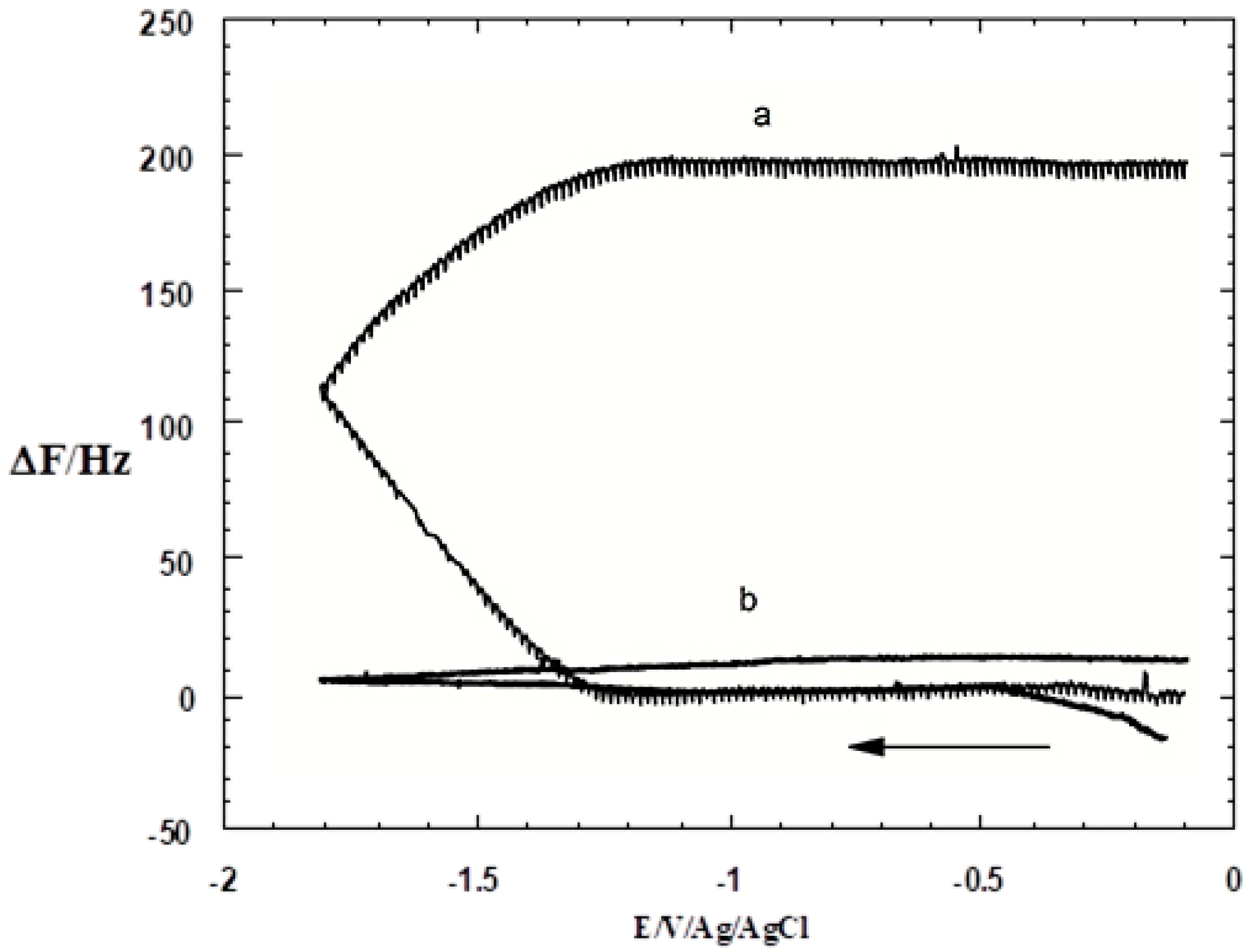
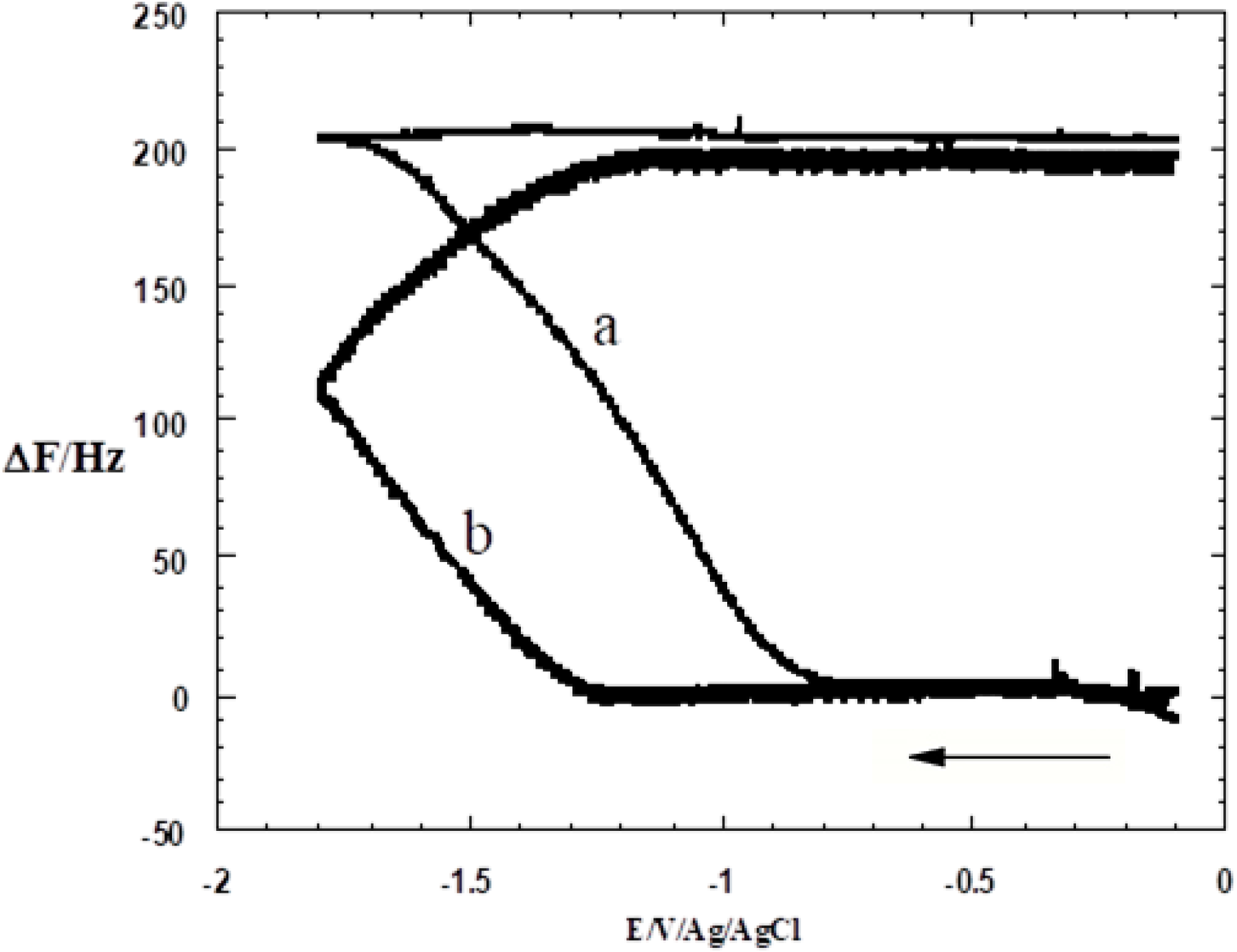
2.4. EQCM Measurement

EQCM measurements were carried out using the basic instrument supplied by Seiko EG&EG (QCA917). The working electrode for the EQCM measurements was a 9 MHz AT-cut quartz crystal with silver electrode furnished by Ditta Nuova Mistral (Latina, Italy). The diameter of the quartz crystal was 14.0 mm, and the silver electrode diameter was 7.4 mm. The area of the working electrode in contact with solution was limited to 0.43 cm2 by an O-ring. The silver electrode on the crystals consisted of 300 nm Ag sputter deposited on an adhesion layer of 50 nm Ti. A suitable flow-cell entirely made of Teflon was designed and realized in the workshop of the Department of Chemistry in Florence. The counter electrode was gold foil, and the reference electrode was an Ag/AgCl sat KCl placed on the outlet tubing of the cell.

2.5. Auger Electron Spectroscopy (AES) Analysis

AES measurements were performed introducing the ex situ prepared samples, in an ultra-high vacuum chamber equipped by a cylindrical mirror analyzer (CMA) with a coaxial electron gun. The spectra were taken in the counting mode. The spectra in the range of 50–600 eV measure the Auger features, namely C KLL, S MLL, Cd MNN and Ag MNN, and have been measured by 1000 and 3000 eV primary electron beams.

3. Results

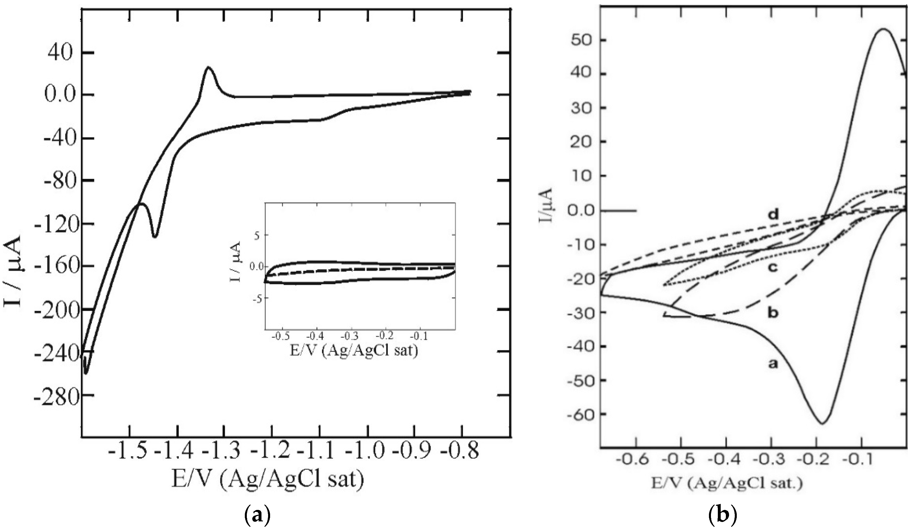
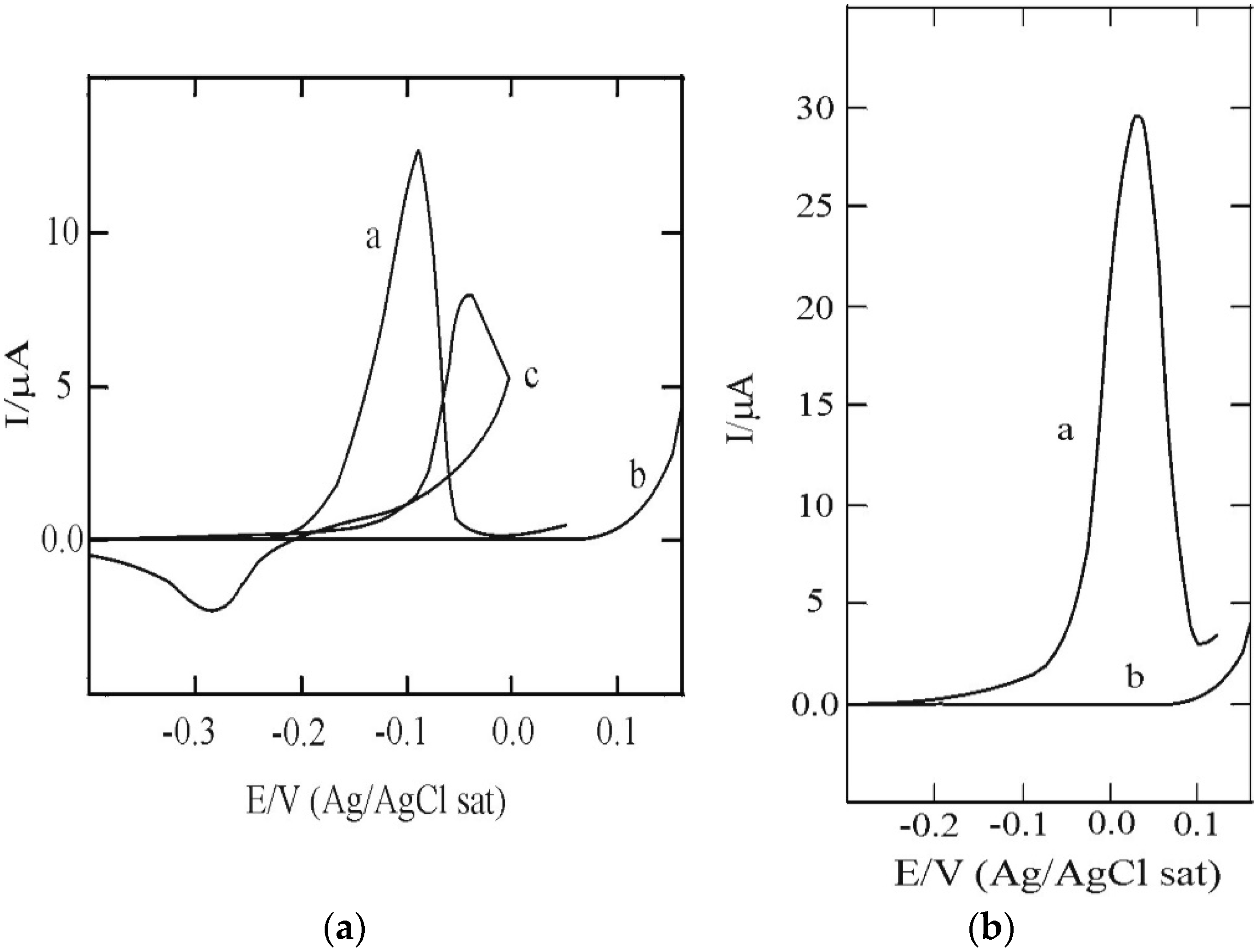
3.1. SAM of C16SH on Ag(III)

In Figure 1a a cyclic voltammogram (CV) of 0.1 mm C16SH on Ag(III) electrodes using 0.1 M NaOH in 95% ethanol and 5% water as recorded from −0.8 V to −1.6 V, after keeping the electrode in the solution for 15 min a second voltammogram was recorded. The second CV overlaps completely with the first, indicating that this time is insufficient to produce significant variation on the amount of adsorbed C16SH. However, even this reduced adsorption time is sufficient to strongly reduce the capacitive current as shown by the flattening of the cyclic voltammogram in the supporting electrolyte (inset of Figure 1a). Moreover, a significant inhibition of the Ru(NH3)63+ reduction is also shown. Figure 1b shows the cyclic voltammograms obtained from 1mm Ru(NH3)63+ in 0.1 M KCl on the bare Ag(III) (curve a), and on Ag(III) covered by C16SH deposited from a 0.03 mm solution for 10 min (curve b), 2 h (curve c) and 26 h (curve d). Similar dependence on the adsorption time was observed for the cyclic voltammograms of Fe(CN)63−/4− on a gold electrode coated by thiols [34]. This behavior is consistent with the kinetic model of thiol adsorption proposed by Nuzzo and coworkers [35].
It must be noted that the curves in Figure 1b were obtained from different experiments, and not in succession. This means that the auto-assembling process was not disturbed at all. Analogous experiments carried out in succession showed that the same degree of inhibition as that shown by curve d is reached after three consecutive 10 min treatments of the electrode.
Unfortunately, the reduction peak of C16SH after SAM formation takes place at potentials similar to those of Figure 1a. The partial overlap with hydrogen evolution hinders the accurate estimation of the charge involved, and hence of the amount of C16SH. Alternatively, the amount of the deposited C16SH can be obtained with electrochemical quartz crystal microbalance (EQCM) measurements by measuring the mass decrease involved in thiol dissolution. Systematic EQCM measurements were performed at increasingly longer modification times. The associated mass variation increases up to reach a limiting value for times greater than 12 h. Repeated washings with ethanol are also necessary to avoid formation of multilayers. Curve a in Figure 2 shows the frequency variation obtained while recording a cyclic voltammogram from −0.1 to −1.8 V. Keeping in mind that a frequency increase corresponds to a mass decrease, it is easy to verify that the SAM layer dissolution starts at −1.25 V. However, in spite of the very low scan rate (2 mV/s), and the very negative final potential, the dissolution process is not yet completed in the forward scan but continues during the backward scan. Curve b in Figure 2 is obtained on a silver electrode not covered by SAM. Both curves were recorded in a 0.1 M NaOH in 95% ethanol and 5% water. By comparison with curve a, the entire frequency variation of the modified electrode seems to be ascribable to thiol dissolution. The mass variation, Δm, is given by the Sauerbrey equation:
Δ f = C f Δ m A
where Δf is the frequency variation, A is the electrode area, and Cf is a coefficient that depends on the quartz properties and on the fundamental resonance frequency. In our case, Cf = 0.183 Hz* cm2/ng, then, the frequency variation involved in curve a of Figure 2 (about 200 Hz for a mass coverage of 3.9 Å2/molecule) gives a mass variation higher than that deduced from the molecular coverage, 18.5 Å2/molecule, found for alkanethiols on Ag(III) [1] and must be considered roughly approximate. The EQCM measurements were performed using commercial polycrystalline silver electrodes (there is no Ag monocrystalline (111) electrode for EQCM that are commercially available) with a very high roughness factor, with the direct consequence of a larger real area respect to the geometrical one. Therefore, the experimental mass variation involved in surface phenomena such as self-assembling is scarcely indicative of what happens on a single crystal. Therefore, rather than to calculate the exact amount of the deposited C16SH, EQCM measurements were performed to establish the time necessary for the complete formation of the SAM, and to constitute a reference for the analogous measurements carried out in the presence of the CdS film, the measured amount of SAM in the two cases are consistent meaning that the system is reproducible even if not approximal to an ideal flat surface.
The slowness of desorption process is confirmed by successive experiments: the silver electrode was modified for 16 h. Then, it was repeatedly treated at E = −1.8 V up to a total time of 8 min. The effect of each potential treatment was verified on a typical surface phenomenon such as the underpotential deposition of sulfur. Figure 3a shows S UPD on a bare Ag(III) electrode, whereas curves a, b and c of Figure 3b are obtained after each potential treatment. The S UPD peak does not increase with further potential treatments. The attainment of a limiting behavior, together with the quasi-complete disappearance of the thiol reduction peak in NaOH 0.1 M, suggests the quasi-complete desorption of the thiol SAM layer. This experiment leads to two considerations. First, it confirms the incomplete dissolution during the forward scan of Figure 2; in fact, at a scan rate of 2 mV/s, it takes about 5 min to cover the potential range −1.25 V ÷ −1.8 V. Secondly, the partial inhibition of S UPD indicates that traces of thiol are still present, even though the EQCM data suggest the complete dissolution.
It is interesting to note that the traces of thiol that are sufficient to inhibit surface phenomena don’t significantly affect redox processes occurring in solution. To this purpose, we performed another experiment: the electrode was modified for 2 h, and subsequently treated at E = −1.6 V for 3 min and then for further 2 min (total time 5 min). Both the shorter time of modification and less negative applied potential were chosen to better scale the experimental results. Then, the UPD of S (Figure 3c) and the reduction curve of Ru(NH3)63+ (Figure 3d) were alternatively recorded. The dashed curves are recorded on the bare Ag(III) electrode; curves a’ and a” on the electrode modified for 2 h; curves b’ and b” after the first treatment at −1.6 V, and curves c’ and c” after the second treatment at −1.6 V. From Figure 3d it is evident that curve c” is not far from the dashed curve, thus indicating that most of the thiol has been removed. At the same time, curve c’ of Figure 3c is much lower than the dashed one, thus again indicating that traces of thiols are sufficient to inhibit surface phenomena such as underpotential depositions, providing to an over estimation of the thiol still present. This result is in good agreement with the observation that n-alkanethiols with n > 6 could remain physisorbed on the terraces [36]. However, our results seem to contradict the possibility of completely removing the physisorbed micelles during electroreduction, at least for C16SH.
The important findings of this experiment are that the criterion for SAM layer formation cannot be based on surface limited phenomena (UPD), because of the interactions with other species on the surface but must be based on the inhibition of the redox processes (Ru3+/Ru2+) occurring in solution, which seems be related only to the area actually available for the reaction. More precisely, curve d in Figure 1b corresponds to the limiting shape of the inhibited process. Note that curve c in Figure 1b, albeit not far from curve d, shows the typical inflection that is characteristic of a SAM layer not yet completed [37].

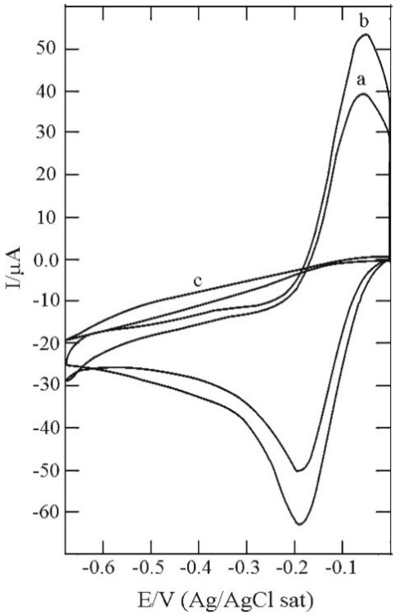
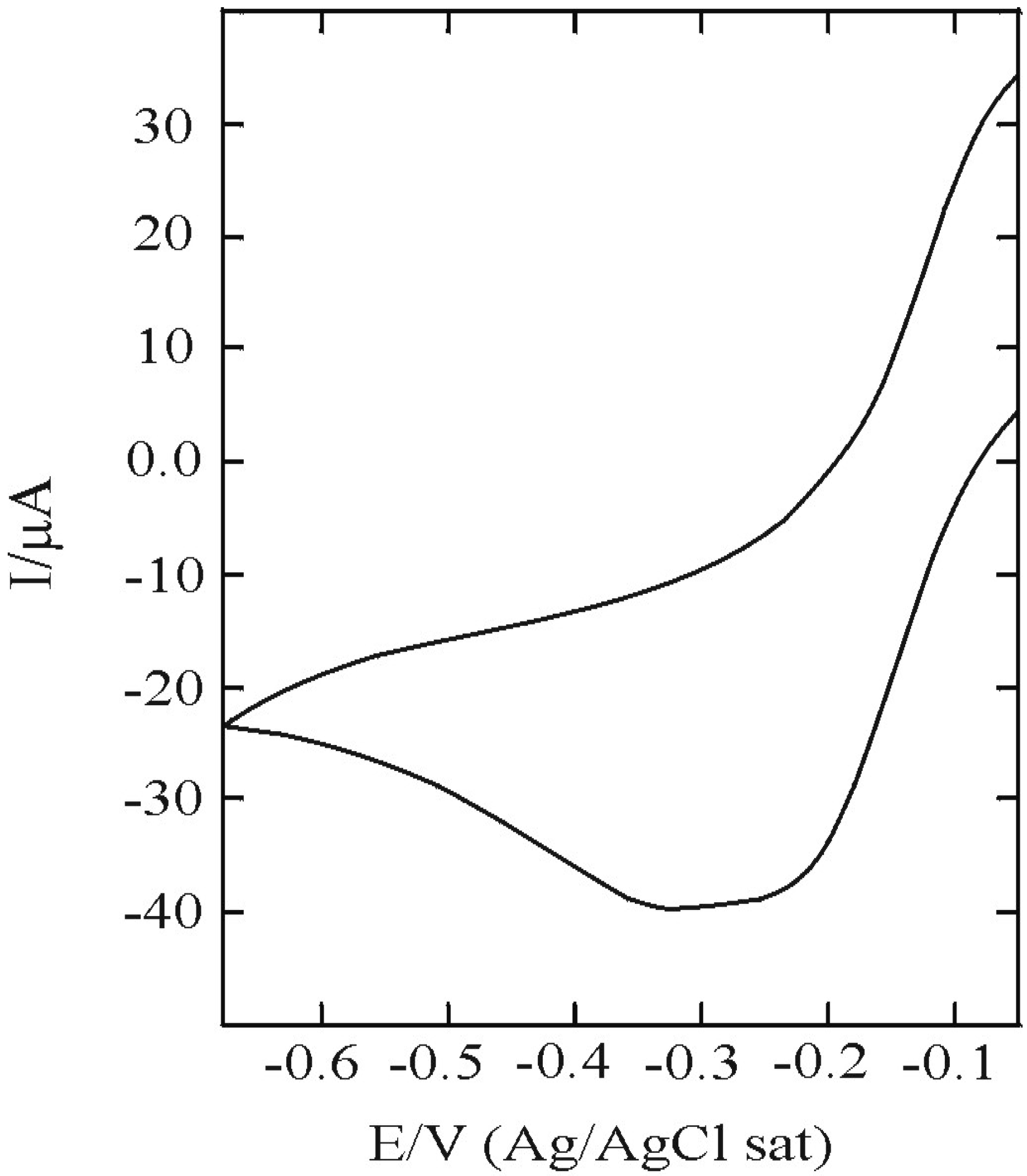
3.2. SAM of C16SH on Ag(III) Covered by an Ultrathin Film of CdS

The first experiments were performed on Ag(III) covered by 10 ECALE cycles of CdS. As stated in the experimental section, the thickness estimated for this deposit is about 2 ÷ 2.5 nm. Curve a in Figure 4 shows the cyclic voltammogram of Ru(NH3)63+ as obtained after having modified this substrate with C16SH for about 26 h. This curve is very close to that obtained on the bare Ag(III) (curve b). The apparent lowering is actually due to the unavoidable decrease of the capacitive contribution due to the SAM layer formation. For a comparison, curve c in the figure is the cyclic voltammogram obtained on a Ag(III) covered by C16SH, which is the same as curve d in Figure 1b.

3.3. C16SH SAM Formation on CdS

Various evidences for SAM formation were obtained. EQCM measurements were performed on a Ag(III) substrate covered by 10 ECALE cycles of CdS and modified with C16SH in the same experimental conditions as those of Figure 2. Figure 5 shows the comparison between the frequency curves obtained in the presence of CdS (curve a) and in the absence (curve b). The almost similar frequency variation suggests that the same amount of C16SH is deposited on the two different substrates. Incidentally, it is interesting to note that the only difference is in a more favored dissolution process of C16SH in the presence of CdS. The reduction process begins to occur at −0.8 V and it is over at −1.7 V. Then, the dissolution process is completed during the forward scan. This observation is in good agreement with the hypothesis of a contrasting behavior, exercised by the presence of CdS, on surface reactivity limited by C16SH. Other evidences for the SAM formation were given by AES measurements. Table 1 reports the film thickness of CdS and C16SH as estimated by the analysis of the attenuated AES signal amplitudes [38,39] of substrates using the electron mean free path database of NIST [40].
The thickness values estimated for the CdS films are in good agreement with the preceding measurements [24]. It must be noted that the C16SH SAM layer thickness on CdS is lower than that on Ag(III), thus suggesting a higher tilt angle. The presence of traces of oxygen (1%) localized on the surface and of a small amount of carbon (3%) probably arising from atmospheric contamination were found. The latter value is difficult to be determined since the C signal is superimposed to the silver peak.
The presence of the intact thiol molecule on Ag(III) and pre-covered CdS Ag(III) samples was verified by X-ray absorption measurements on the C K-edge and S L2,3 edges and will be discussed in a forthcoming paper.
Both EQCM and AES measurements confirm the presence of the C16SH SAM layer. However, none of them are able to detect details of the maximum coverage and the structure of SAM layer. This latter measurement is provided by the inhibition of the stripping peak of Cd from the CdS deposit covered by C16SH. Curve a in Figure 6a is the stripping peak of Cd from CdS deposited on Ag(III) with 10 ECALE cycles. When such a substrate was modified with C16SH for about 18 h, the dissolution of Cd is completely hindered (curve b). For a comparison, curve c refers to only a partial formation of SAM, as obtained when the substrate was modified for insufficiently long times. In this case, the stripping peak is only partially inhibited. The stripping of Cd occurs at potentials progressively more positive as the number of ECALE cycles is increased. Curve a in Figure 6b is the stripping curve of Cd from CdS deposited with 30 ECALE cycles and curve b shows again the blocking effect of the thiol SAM Layer.
It must be noted that the described behavior indicates that the thiol SAM physically blocks the underlying CdS deposits. From this point of view, the possibility that curve a of Figure 4 was simply due to a total or partial SAM removal and that, therefore, the effect of CdS was only apparent, has to be disregarded. In fact, any partial Cd dissolution from the underlying CdS deposit should distort the reduction curve of Ru(NH3)63+. As an example, Figure 7 shows the cyclic voltammogram of Ru(NH3)63+ on a silver electrode covered by 30 ECALE cycles of CdS not protected by the thiol. The slightly positive current at the initial potential E = −0.08 V indicates that a small amount of Cd is dissolved, what was reasonably expected on the basis of curve a of Figure 6b. This amount of dissolved Cd is again reduced during the negative scan, giving rise to the small bump at about −0.33 V.

3.4. Estimate of the SAM Layer Quality

An exhaustive discussion on the criteria used for defect level assessment is given by Miller et al. in reference [12]. Here, electron tunneling through the full thickness of self-assembled organic monolayers of ω–hydroxy thiols is demonstrated. Briefly, the possibility of either small pinholes exposing the electrode surface or collapse sites [21] causing the monolayer to be significantly thinner than the bulk monolayer SAM layer are taken into account. Because of the strong dependence of the electron transfer kinetic on the thickness of the insulating SAM layer, even a small coverage of such defects could be entirely responsible for the current measured. In order to assess the effect of such defects, Miller et al. used the theoretical model of Amatore et al. for the redox kinetics at partially blocked electrodes [37]. According to this model, the presence of pinholes or collapse sites separated by distances greater than the characteristic diffusion length of the experiment (which, in our experiments, is in the order of tens of microns) should give rise to sigmoidal voltammetric waves characteristic of an array of microelectrodes. The behavior as an array of microelectrodes was also obtained after having deliberately perforated monolayers-coated electrodes [41]. As a matter of fact, in our experiments, sigmoidal waves were only observed with insufficient modification time (see for instance curve c of Figure 1b). On the other hand, the presence of defects separated by distances smaller than the characteristic diffusion length should give rise to voltammetric curves indistinguishable in shape from those obtained at electrodes with continuous insulating layer.
Further evidences were obtained by modifying the Ag(III) covered by 30 ECALE cycles of CdS for increasing time, in a way similar to the experiment of Figure 3. The thicker CdS film is necessary to limit Cd dissolution during the recording of Ru(NH3)63+ cyclic voltammogram. Figure 8a. shows the curves of Ru(NH3)63+ obtained after having modified the electrode for 20 min (curve a), 30 min (curve b), 90 min (curve c) and 4 h (curve d). Surprisingly, the redox process shows an inhibition effect that increases with the adsorption time. This result is in contrast with curve a of Figure 4 obtained after having modified the substrate for 17 h. However, a further modification of 17 h yielded the dashed curve in Figure 8a. This latter curve, although not coincident with curve a of Figure 4, indicates a reversed trend. This behavior is consistent with a higher level of order ensured by the additional modification time. Then, it is reasonable to assume that the occurring of charge transfer is connected to the order of the SAM rather than to the adsorption time.
As a matter of fact, curve a in Figure 8b shows the Ru(NH3)63+ reduction peak obtained on Ag(III) covered by 30 ECALE cycles and modified for a time (3 h), which, according to Nuzzo and co-workers [35], is surely insufficient to produce an ordered monolayer. The Ru(NH3)63+ reduction is much less inhibited than in the experiments of Figure 8a. At the same time it is much more inhibited that in the presence of a SAM formed on a similar substrate with an adsorption time longer than 12 h (curve b). To avoid Cd dissolution, the initial potential was shifted to −0.05 V. Then, it is reasonable to assume that the necessary condition for charge transfer is that the monolayer is ordered.

4. Conclusions

The behavior of self-assembled monolayers of 1-hexanedecanthiol (C16SH) formed on Ag(III) covered by ultrathin films of CdS was compared with that of analogous SAMs formed on the bare Ag(III). The strong insulating effect of C16SH deposited on Ag(III) is shown by the inhibition of the voltammetric peak of Ru(NH3)63+/2+. On the contrary, the voltammogram obtained on Ag(III) covered by an ultrathin film of CdS is very similar to that obtained on the bare Ag(III) electrode. The crucial point of our work is to demonstrate the effective formation of C16SH monolayers on Ag(III) covered by CdS. A number of different experiments were performed to confirm the presence of C16SH. In particular, EQCM measurements revealed that an identical mass decrease is involved in thiol dissolution both in the presence and in the absence of CdS. Then, AES measurements confirmed the presence of C16SH SAM layer both on Ag(III) and on CdS. The thickness of the SAM layer formed on CdS, 20 Å, is lower than that of the SAM layer formed on Ag(III), 25 Å, thus indicating a higher tilt angle.
Neither EQCM nor AES are able to detect the formation of a complete SAM layer of thiol. However, the evidence for a well-formed SAM layer is given by the physical blocking of the stripping peak of Cd from the CdS deposit covered by C16SH. For this reason, only partial inhibition of the Cd stripping peak is observed with SAM layer of C16SH obtained with not sufficiently long adsorption times. Moreover, the presence of the intact thiol molecule on Ag(III) and pre-covered CdS Ag(III) samples was verified by X-ray absorption measurements on the C K-edge and S L2,3 edges and will be discussed in a forthcoming paper.
Our results suggest that self-assembly on semiconductors could become interesting whenever a charge transfer is required. As an example, they could be used to anchor molecules that change their properties following an electrochemical reduction or oxidation. The hypothesis that the observed behavior was simply due to a total or partial SAM removal and that, therefore, the effect of CdS was only apparent, has to be disregarded, since in this case the concomitant CdS dissolution should be observed.
While the structure of thiols on Ag(III) is known to give well packed and ordered structures [1,2,16,17,31], none of the measurements presented here allow us to determine the exact structure or degree of crystallinity of the SAM layers obtained in the presence of CdS. Our results on the occurrence of electron transfer are purely phenomenological, since they are limited to the system studied, particularly Ag(III) covered by n-CdS using a reduction process such as that of Ru(NH3)63+. Any interpretation would require the extension of the measurements to other substrates (for example gold) and to other semiconductors (for example other II–VI or III–V compound semiconductors both n-type and p-type). Finally, other electrochemical probes, such as Fe(CN)63− or Fe(CN)64−, should be used to explore possible discrepancies towards reduction or oxidation processes.

Author Contributions

Funding acquisition, S.C.; Investigation, W.G., M.P. (Maurizio Passaponti), L.F. and P.M.; Methodology, M.L.F., S.M. and N.C.; Supervision, M.P. (Maddalena Pedio) and M.I.; Writing-original draft, E.S.

Acknowledgments

The authors are grateful to Ferdinando Capolupo for the preparation of the silver single crystal electrodes. The technical services of TASC laboratory are kindly acknowledged. The financial support of the Italian CNR, of the Murst and of the Consorzio Interuniversitario per la Scienza e Tecnologia (INSTM) is gratefully acknowledged. We are also grateful to Regione Toscana—Programma Operativo Regionale POR FESR Toscana 2014–2020, BANDO N. 2: Progetti di ricerca e sviluppo delle MPMI, Project GADGET “Gioielli in Argento da Galvanica, Ecologica e Tecnologica”.

Conflicts of Interest

The authors declare no conflicts of interest.

References

  1. Schreiber, R. Structure and growth of self-assembled monolayers. Prog. Surf. Sci. 2000, 65, 151–256. [Google Scholar] [CrossRef]
  2. Ulman, A. Formation and structure of self-assembled monolayers. Chem. Rev. 1996, 96, 1533–1554. [Google Scholar] [CrossRef] [PubMed]
  3. Gu, Y.; Lin, Z.; Butera, R.A.; Smentkowski, V.S.; Waldeck, D.H. Preparation of Self-Assembled Monolayers on InP. Langmuir 1995, 11, 1849–1851. [Google Scholar] [CrossRef]
  4. Gu, Y.; Waldeck, D.H. Studies of electron tunneling at semiconductor electrodes. J. Phys. Chem. 1996, 100, 9573–9576. [Google Scholar] [CrossRef]
  5. Gu, Y.; Kumar, K.; Read, I.; Zimmt, M.B. Studies into the character of electronic coupling in ectron transfer. J. Photochem. Photobiol. A 1997, 105, 189–196. [Google Scholar] [CrossRef]
  6. Gu, Y.; Waldeck, D.H. Electron Tunneling at the Semiconductor−Insulator−Electrolyte Interface. Photocurrent Studies of the n-InP−Alkanethiol−Ferrocyanide System. J. Phys. Chem. B 1998, 102, 9015–9028. [Google Scholar] [CrossRef]
  7. Sheen, C.W.; Shi, J.X.; Martensson, J.; Parikh, A.N.; Allara, D.L. A New Class of Organized Self-Assembled Monolayers: Alkane Thiols on GaAs(100). J. Am. Chem. Soc. 1992, 114, 1514–1515. [Google Scholar] [CrossRef]
  8. Baum, T.; Ye, S.; Uosaki, K. Formation of Self-Assembled Monolayers of Alkanethiols on GaAs Surface with in Situ Surface Activation by Ammonium Hydroxide. Langmuir 1999, 15, 8577–8579. [Google Scholar] [CrossRef]
  9. Ye, S.; Li, G.; Noda, H.; Uosaki, K.; Osawa, M. Characterization of self-assembled monolayers of alkanethiol on GaAs surface by contact angle and angle-resolved XPS measurements. Surf. Sci. 2003, 529, 163–170. [Google Scholar] [CrossRef]
  10. Kosuri, M.R.; Cone, R.; Li, Q.; Han, S.M.; Bunker, B.C.; Mayer, T.M. Adsorption kinetics of 1-alkanethiols on hydrogenated Ge(111). Langmuir 2004, 20, 835–840. [Google Scholar] [CrossRef] [PubMed]
  11. Porter, M.D.; Bright, T.B.; Allara, D.L.; Chidsey, C.E.D. Spontaneously organized molecular assemblies. 4. Structural characterization of n-alkyl thiol monolayers on gold by optical ellipsometry, infrared spectroscopy, and electrochemistry. J. Am. Chem. Soc. 1987, 109, 3559–3568. [Google Scholar] [CrossRef]
  12. Miller, C.; Cuendet, P.; Graetzel, M. Adsorbed .omega.-hydroxy thiol monolayers on gold electrodes: Evidence for electron tunneling to redox species in solution. J. Phys. Chem. 1991, 95, 877–886. [Google Scholar] [CrossRef]
  13. Miller, C.; Graetzel, M. Electrochemistry at .omega.-hydroxythiol coated electrodes. 2. Measurement of the density of electronic states distributions for several outer-sphere redox couples. J. Phys. Chem. 1991, 95, 5225–5233. [Google Scholar] [CrossRef]
  14. Becka, A.M.; Miller, C.J. Electrochemistry at .omega.-hydroxy thiol coated electrodes. 3. Voltage independence of the electron tunneling barrier and measurements of redox kinetics at large overpotentials. J. Phys. Chem. 1992, 96, 2657–2668. [Google Scholar] [CrossRef]
  15. Terrettaz, S.; Becka, A.M.; Traub, M.J.; Fettinger, J.C.; Miller, C.J. .omega.-Hydroxythiol Monolayers at Au Electrodes. 5. Insulated Electrode Voltammetric Studies of Cyano/Bipyridyl Iron Complexes. J. Phys. Chem. 1995, 99, 11216–11224. [Google Scholar] [CrossRef]
  16. Hatchett, D.W.; Uibel, R.H.; Stevenson, K.J.; Harris, J.M.; White, H.S. Electrochemical measurement of the free energy of adsorption of n-alkanethiolates at Ag(111). J. Am. Chem. Soc. 1998, 120, 1062–1069. [Google Scholar] [CrossRef]
  17. Azzaroni, O.; Vela, M.E.; Andreasen, G.; Carro, P.; Salvarezza, R.C. Electrodesorption potentials of self-assembled alkanethiolate monolayers on Ag(111) and Au(111). An electrochemical, scanning tunneling microscopy and density functional theory study. J. Phys. Chem. B 2002, 106, 12267–12273. [Google Scholar] [CrossRef]
  18. Lee, T.; Wang, W.; Reed, M.A. Mechanism of Electron Conduction in Self-Assembled Alkanethiol Monolayer Devices. Ann. N. Y. Acad. Sci. 2003, 1006, 21–35. [Google Scholar] [CrossRef] [PubMed]
  19. Krysiński, P.; Brzostowska-Smolska, M. Three-probe voltammetric characterisation of octadecanethiol self-assembled monolayer integrity on gold electrodes. J. Electroanal. Chem. 1997, 424, 61–67. [Google Scholar] [CrossRef]
  20. Finklea, H.O.; Robinson, L.R.; Blackburn, A.; Richter, B.; Allara, D.; Bright, T. Formation of an Organized Monolayer by Solution Adsorption of Octadecyltrichlorosilane on Gold: Electrochemical Properties and Structural Characterization. Langmuir 1986, 2, 239–244. [Google Scholar] [CrossRef]
  21. Finklea, H.O.; Avery, S.; Lynch, M.; Furtsch, T. Blocking oriented monolayers of alkyl mercaptans on gold electrodes. Langmuir 1987, 3, 409–413. [Google Scholar] [CrossRef]
  22. Innocenti, M.; Pezzatini, G.; Forni, F.; Foresti, M.L. CdS and ZnS Deposition on Ag(111) by Electrochemical Atomic Layer Epitaxy. J. Electrochem. Soc. 2001, 148, C357–C362. [Google Scholar] [CrossRef]
  23. Cecconi, T.; Atrei, A.; Bardi, U.; Forni, F.; Innocenti, M.; Loglio, F.; Foresti, M.L.; Rovida, G. X-ray photoelectron diffraction (XPD) study of the atomic structure of the ultrathin CdS phase deposited on Ag(111) by electrochemical atomic layer epitaxy (ECALE). J. Electron Spectros. Relat. Phenom. 2001, 114–116, 563–568. [Google Scholar] [CrossRef]
  24. Innocenti, M.; Cattarin, S.; Cavallini, M.; Loglio, F.; Foresti, M.L. Characterisation of thin films of CdS deposited on Ag(111) by ECALE. A morphological and photoelectrochemical investigation. J. Electroanal. Chem. 2002, 532, 219–225. [Google Scholar] [CrossRef]
  25. Innocenti, M.; Forni, F.; Pezzatini, G.; Raiteri, R.; Loglio, F.; Foresti, M.L. Electrochemical behavior of As on silver single crystals and experimental conditions for InAs growth by ECALE. J. Electroanal. Chem. 2001, 514, 75–82. [Google Scholar] [CrossRef]
  26. Foresti, M.L.; Milani, S.; Loglio, F.; Innocenti, M.; Pezzatini, G.; Cattarin, S. Ternary CdSxSe1−x deposited on Ag(111) by ECALE: Synthesis and characterization. Langmuir 2005, 21, 6900–6907. [Google Scholar] [CrossRef] [PubMed]
  27. Loglio, F.; Innocenti, M.; D’Acapito, F.; Felici, R.; Pezzatini, G.; Salvietti, E.; Foresti, M.L. Cadmium selenide electrodeposited by ECALE: Electrochemical characterization and preliminary results by EXAFS. J. Electroanal. Chem. 2005, 575, 161–167. [Google Scholar] [CrossRef]
  28. Cavallini, M.; Facchini, M.; Albonetti, C.; Biscarini, F.; Innocenti, M.; Loglio, F.; Salvietti, E.; Pezzatini, G.; Foresti, M.L. Two-dimensional self-organization of CdS ultra thin films by confined electrochemical atomic layer epitaxy growth. J. Phys. Chem. C 2007, 111, 1061–1064. [Google Scholar] [CrossRef]
  29. Wang, L.; Bevilacqua, M.; Chen, Y.X.; Filippi, J.; Innocenti, M.; Lavacchi, A.; Marchionni, A.; Miller, H.; Vizza, F. Enhanced electro-oxidation of alcohols at electrochemically treated polycrystalline palladium surface. J. Power Sources 2013, 242, 872–876. [Google Scholar] [CrossRef]
  30. Gregory, B.W.; Stickney, J.L. Electrochemical atomic layer epitaxy (ECALE). J. Electroanal. Chem. Interfacial Electrochem. 1991, 300, 543–561. [Google Scholar] [CrossRef]
  31. Azzaroni, O.; Schilardi, P.L.; Salvarezza, R.C. Metal electrodeposition on self-assembled monolayers: A versatile tool for pattern transfer on metal thin films. Electrochim. Acta 2003, 48, 3107–3114. [Google Scholar] [CrossRef]
  32. Foresti, M.L.; Capolupo, F.; Innocenti, M.; Loglio, F. Visual Detection of Crystallographic Orientations of Face-Centered Cubic Single Crystals. Cryst. Growth Des. 2002, 2, 73–77. [Google Scholar] [CrossRef]
  33. White, R.E.; Bockris, J.O.; Conway, B.E. Modern Aspects of Electrochemistry; Springer: New York, NY, USA, 1995; ISBN 978-1-4899-1726-3. [Google Scholar]
  34. Diao, P.; Jiang, D.; Cui, X.; Gu, D.; Tong, R.; Zhong, B. Studies of structural disorder of self-assembled thiol monolayers on gold by cyclic voltammetry and ac impedance. J. Electroanal. Chem. 1999, 464, 61–67. [Google Scholar] [CrossRef]
  35. Bain, C.D.; Troughton, E.B.; Tao, Y.T.; Evall, J.; Whitesides, G.M.; Nuzzo, R.G. Formation of monolayer films by the spontaneous assembly of organic thiols from solution onto gold. J. Am. Chem. Soc. 1989, 111, 321–335. [Google Scholar] [CrossRef]
  36. Vericat, C.; Andreasen, G.; Vela, M.E.; Martin, H.; Salvarezza, R.C. Following transformation in self-assembled alkanethiol monolayers on Au(111) by in situ scanning tunneling microscopy. J. Chem. Phys. 2001, 115, 6672–6678. [Google Scholar] [CrossRef]
  37. Amatore, C.; Savéant, J.M.; Tessier, D. Charge transfer at partially blocked surfaces: A model for the case of microscopic active and inactive sites. J. Electroanal. Chem. Interfacial Electrochem. 1983, 147, 39–51. [Google Scholar] [CrossRef]
  38. Seah, P.M.; Dench, A.W. Quantitative electron spectroscopy of surfaces: A standard data base for electron inelastic mean free paths in solids. Surf. Interface Anal. 1979, 1, 2–11. [Google Scholar] [CrossRef]
  39. Woodruff, D.P.; Delchar, T.A. Modern Techniques of Surface Science; Cambridge Solid State Science Series; Cambridge Univercity Press: Cambridge, UK, 1986. [Google Scholar]
  40. Powell, C.J.; Jablonski, A. NIST Electron Inelastic-Mean-Free-Path Database; U.S. Department of Commerce: Washington, DC, USA, 2010.
  41. Finklea, H.O.; Snider, D.A.; Fedyk, J.; Sabatani, E.; Gafni, Y.; Rubinstein, I. Characterization of Octadecanethiol-Coated Gold Electrodes as Microarray Electrodes by Cyclic Voltammetry and ac Impedance Spectroscopy. Langmuir 1993, 9, 3660–3667. [Google Scholar] [CrossRef]
Figure 1. (a) Cyclic voltammograms of 0.1 mm C16SH on Ag(III) electrodes using 0.1 M NaOH in 95% ethanol and 5% water as recorded from −0.8 V to −1.6 V/Ag/AgCl sat; inset: cyclic voltammogram of a bare Ag(III) (solid curve) and on Ag(III) modified for 15 min in C16SH solution (dashed curve); (b) cyclic voltammograms obtained from 1 mm Ru(NH3)63+ in 0.1 M KCl on the bare Ag(III) (curve a), and on Ag(III) covered by C16SH deposited from a 0.03 mm solution for 10 min (curve b), 2 h (curve c) and 26 h (curve d). The scan rate was 50 mV/s.
Surfaces 01 00004 g001
Figure 2. Frequency change during a single potential scan from −0.1 to 1.8 V recorded on the silver EQCM electrode modified with C16SH for times greater than 12 h (curve a) and on a silver electrode not covered by SAM (curve b). Both curves were recorded in a 0.1 M NaOH in 95% ethanol and 5% water. The scan rate was 2 mV/s.
Surfaces 01 00004 g002
Figure 3. (a) Oxidative UPD of S on Ag(III) from 1 mm Na2S, as recorded from −1.1 to −0.68 V; (b) oxidative UPD of S on Ag(III) modified with C16SH for 16 h and successively treated at at E = −1.8 for 1 min (curve a), 3 min (curve b) and 4 min (curve c) up to a total time of 8′; (c) oxidative UPD of S on Ag(III) modified with C16SH for 2 h (curve a’) and successively treated at E = −1.6 V for 3 min (curve b’) and further 2 min (curve c’) up to a total time of 5 min; as comparison, the dashed curve is the curve on the bare Ag(III); (d) cyclic voltammograms obtained from 1 mm Ru(NH3)63+ in 0.1 M KCl on Ag(III) modified with C16SH for 2 h (curve a”) and successively treated at E = −1.6 V for 3 min (curve b”) and further 2 min (curve c”) up to a total time of 5 min; as comparison, the dashed curve is the curve on the bare Ag(III). All curves were recorded in pH 9.2 ammonia buffer solutions. The scan rate was 50 mV/s.
Surfaces 01 00004 g003aSurfaces 01 00004 g003b
Figure 4. Cyclic voltammograms obtained from 1 mm Ru(NH3)63+ in 0.1 M KCl on Ag(III) covered by 10 ECALE cycles and modified with C16SH for 26 h (curve a), on bare Ag(III) (curve b), and on Ag(III) modified with C16SH in the absence of CdS (curve c).The scan rate was 50 mV/s.
Surfaces 01 00004 g004
Figure 5. Frequency change during a single potential scan from −0.1 to 1.8 V recorded on the silver EQCM electrode modified with C16SH for times greater than 12 h in presence of CdS (curve a) and in the absence (curve b). The scan rate was 2 mV/s.
Surfaces 01 00004 g005
Figure 6. (a) Linear sweep voltammograms for the oxidative strippings of Cd from CdS deposited with 10 ECALE cycles on Ag(III) not covered by thiol (curve a); modified for about 18 h (curve b) and modified for short times (curve c); (b) linear sweep voltammograms for the oxidative strippings of Cd from CdS deposited with 30 ECALE cycles on Ag(III) not covered by thiol (curve a); modified for about 18 h (curve b). The scan rate was 10 mV/s.
Surfaces 01 00004 g006
Figure 7. Cyclic voltammograms obtained from 1 mm Ru(NH3)63+ in 0.1 M KCl on Ag(III) covered by 30 ECALE cycles in the absence of thiol. The scan rate was 50 mV/s.
Surfaces 01 00004 g007
Figure 8. (a) Cyclic voltammograms obtained from 1 mm Ru(NH3)63+ in 0.1 M KCl on Ag(III) covered by 30 ECALE cycles and modified with C16SH for 20 min (curve a), 30 min (curve b), 90 min (curve c) and 4 h (curve d); the dashed curve was obtained after having further modified the substrate for 17 h; (b) cyclic voltammograms obtained from 1 mm Ru(NH3)63+ in 0.1 M KCl on Ag(III) covered by 30 ECALE cycles and modified with C16SH for 3 h (curve a), and more than 12 h (curve b).The scan rate was 50 mV/s.
Surfaces 01 00004 g008
Table 1. Film thicknesses of CdS and C16SH as estimated by the analysis of the attenuated AES signal amplitudes using the electron mean free path database of NIST.
SampleTotal Thickness (Å)CdS Thickness (Å)C16SH Thickness (Å)
30 CdS/Ag(III)85 + 775 + 10-
C16SH/Ag(III)25 + 5-25 + 5
C16SH + 10CdS/Ag(III)40 + 620 + 320 + 3
C16SH + 30CdS/Ag(III)88 + 868 + 720 + 3

