
First Results of Nb3Sn Coated Cavity by Vapor Diffusion Method at SARI
by
 , , and
Qixin Chen
1,2, 
Yue Zong
1,2,
Zheng Wang
1,2,
Shuai Xing
3,
Jiani Wu
3,
Pengcheng Dong
3,
Miyimin Zhao
4,
Xiaowei Wu
5,
Jian Rong
6 and
Jinfang Chen
1,2,3,4,* 1
Shanghai Institute of Applied Physics, Chinese Academy of Sciences, Shanghai 201800, China
2
University of Chinese Academy of Sciences, Beijing 100049, China
3
Shanghai Advanced Research Institution, Chinese Academy of Sciences, Shanghai 201210, China
4
School of Physical Science and Technology, ShanghaiTech University, Shanghai 201210, China
5
Zhangjiang Laboratory, Shanghai 201210, China
6
School of Nuclear Science and Technology, Lanzhou University, Lanzhou 730000, China
*
Author to whom correspondence should be addressed.
Coatings 2024, 14(5), 581; https://doi.org/10.3390/coatings14050581
Submission received: 7 April 2024
/
Revised: 29 April 2024
/
Accepted: 3 May 2024
/
Published: 7 May 2024
(This article belongs to the Section Surface Characterization, Deposition and Modification)
Abstract
:Nb3Sn is emerging as one of the focal points in superconducting radio frequency (SRF) research, owing to its excellent superconducting properties. These properties hold significant possibilities for cost reduction and the miniaturization of accelerators. In this paper, we report the recent efforts of the Shanghai Advanced Research Institute (SARI) in fabricating high-performance Nb3Sn superconducting cavities using the vapor diffusion method. This includes the construction of a Nb3Sn coating system with dual evaporators and the test results of 1.3 GHz single-cell coated cavities. The coated samples were characterized, and the growth state of the Nb3Sn films was analyzed. The first coated superconducting cavity was tested at both 4.4 K and 2 K, with different cooldown rates passing through the Nb3Sn critical temperatures. The causes of Sn droplet spot defect formation on the surface of the first cavity were analyzed, and such defects were eliminated in the coating of the second cavity by controlling the evaporation rate. This study provides a reference for the preparation of high-performance Nb3Sn-coated cavities using the vapor diffusion method, including the setup of the coating system, the comprehension of the vapor diffusion process, and the test conditions.
1. Introduction
Superconducting radio frequency cavities are widely used in particle accelerators [1,2,3,4] such as CEBAF, XFEL, LCLS II, and SHINE. The primary performance parameters for superconducting cavities are the intrinsic quality factor () and accelerating gradient () [5]. A higher expresses lower power dissipated within a superconducting radio frequency (SRF) cavity, which is linked to cavity material properties, operating temperature, and frequency, among other factors. A higher corresponds to a shorter accelerating structure required to achieve a specific particle energy. The theoretical maximum is associated with the peak surface magnetic field () inside the cavity. Regarding an ideal defect-free surface, the maximum value of depends on the superheating field () of the cavity material. Exceeding this maximum value allows external flux to penetrate the superconductor, leading to the loss of superconductivity [6,7]. Currently, most SRF cavities utilize pure niobium as material [8,9]. With advancements in manufacturing and surface treatment technologies, the performance of the niobium cavity has approached its theoretical limits [10,11,12,13]. Consequently, there is a growing focus on exploring new generations of SRF materials. Several alternative materials exhibit superior properties compared with Nb, such as Nb3Sn, NbN, and MgB2 [14,15,16].
Nb3Sn stands out as one of the most promising materials with a theoretical superheating magnetic field of 430 mT, approximately double that of niobium. This suggests that a Tesla-shape superconducting cavity constructed with Nb3Sn could achieve a maximal at around 100 MV/m. Additionally, Nb3Sn maintains a high critical temperature of 18.3 K, enabling superconducting cavities made of Nb3Sn to theoretically attain over 1010 at 4.2 K, comparable to Nb cavities operating at 2 K. This shows significant potential for simplifying cooling systems and downsizing accelerators [17,18]. However, Nb3Sn does have some disadvantages, including low thermal conductivity and a brittle texture, leading to difficulties in the fabrication of SRF cavities. Therefore, the current optimal solution is using Nb3Sn as a coating material on the inner surfaces of niobium or copper cavities to address these issues. Various methods are applied for preparing Nb3Sn-coated cavities, including vapor diffusion [19], magnetron sputtering [20], the bronze process [21], electrochemical plating [22], and chemical vapor deposition [23]. Among them, the vapor diffusion method demonstrates the most effective application effect so far.
In 1954, Nb3Sn was first discovered to exhibit superconductivity [24], and by 1961, it was considered in fabricating superconducting RF cavities. In 1962, Saur and Wurm developed the vapor diffusion method to produce Nb3Sn [25]. By the 1970s, Siemens had successfully applied this method to produce TE and TM-mode Nb3Sn cavities, achieving the highest peak surface magnetic field ever recorded for an X-band TE-mode cavity [26]. However, due to a limited understanding of the SRF mechanism and cavity treatment technology constraints, the challenging Q-slope issue in Nb3Sn cavities remained unsolved until the 2000s, which hindered research progress. Subsequently, with advancements in bulk niobium SRF cavity treatment techniques and enlightening of the theory of the superheating field, Cornell University resumed research on coating Nb3Sn cavities using vapor diffusion in 2009 [19]. The researchers constructed a deposition system, customized a standard coating recipe based on Wuppertal’s formula, and successfully overcame limitations to produce Nb3Sn cavities that could be applied in practice. Soon after, several laboratories, such as Jefferson Lab [27], Fermi National Accelerator Laboratory [28], KEK [29], Peking University [30], IMP [31], and IHEP [32] joined the research.
In this study, we constructed the first dual evaporation source coating device for 1.3 GHz single-cell Tesla-shape SRF cavities. We fabricated two single-cell Nb3Sn coated cavities using the vapor diffusion method and tested them at different cooling rates to illustrate the effect of the cooling rate. Additionally, we investigated the formation of speckle defects that appeared in the first cavity. These defects were eliminated by controlling the evaporation intensity during the coating of the second cavity, resulting in an improvement in its performance.
2. Experiment
2.1. Research Method
The vapor diffusion method, also known as physical vapor deposition (PVD) technology, involves the vaporization of pure Sn from the evaporation source at a certain temperature. Then, the vapor diffuses onto the inner surface of the superconducting cavities and reacts with the Nb in the substrate to form Nb3Sn thin films. The entire process occurs within an ultra-high-vacuum (UHV) furnace, as shown in Figure 1.
The growth of Nb3Sn during the coating process, as illustrated in Figure 2, is primarily divided into two stages: nucleation and film growth [5]. During the initial nucleation stage, the decomposition of an additional nucleating agent (SnCl2 or SnF2) results in high vapor pressure, leading to the formation of numerous Sn embryos on the surface. As the temperature increases, Sn diffuses into the Nb substrate and Nb3Sn crystals form. These crystals continuously assimilate atoms from the vapor and grow to be thin films. Subsequently, the deposited Sn atoms mainly diffuse into the Nb3Sn–Nb interface and Nb substrate through grain boundaries, allowing the film to continue growing until the heating process concludes.
2.2. Preparation of the Coated Cavities
In order to study the Nb3Sn cavities, SARI constructed a specialized coating system [34]. The ultra-high-vacuum furnace of this coating system comprises two primary components: a commercially customized high-vacuum furnace, which offers a clean and efficient heating environment, and an additional chamber made of pure Nb with a residual resistivity ratio (RRR) of ~40. This Nb chamber isolates the main reaction area and separates the vapor from the furnace heater. This design aims to prevent potential contamination and to increase the lifetime of the coating system. In order to achieve a more uniform growth of the final film, a dual evaporation source was introduced into the single-cell cavity coating device, and a horizontal furnace was used to accommodate a particular Nb cavity–Sn evaporator configuration, although it presented a more complicated implementation. A detailed structural diagram is shown in Figure 3, and the main design specifications are listed in Table 1.
The outer shell of the heating furnace is made of stainless steel. It can reach a maximum heating temperature of 1400 °C, with three independently controlled heaters. One of them heats the coating chamber, forming a Ø600 mm × 1000 mm hot zone, which is realized by Mo flat elements attached to the inner wall of the furnace. The other two independent heaters are inside the coating chamber and control the temperature of the evaporation sources. These heaters, consisting of Wu bars and ceramic housings, surround the crucible and form a uniform effective hot zone for heating. The coating chamber is made of a 4 mm thick pure Nb plate rolled into a cylinder and welded with an electron beam. It is placed on a Mo–La alloy bracket in the furnace with Nb–Ti flanges at both sides to provide support with sufficient strength. One of them links to the furnace door, and the other is connected to the pump group with bellows, which provides longitudinal protection for the expansion of the chamber during heating. The chamber is equipped with Nb brackets to support the crucible heater and the superconducting cavities, and heat shields are installed at both ends of the chamber to efficiently construct the heating region and ensure temperature uniformity. The configuration of two evaporation sources used in this coating apparatus has previously only been used in FERMILAB for 9-cell cavity coating [5]; unlike other single-cell cavity-coating systems in other laboratories [29,30,31,32], it ensures uniform vapor flow and potentially improves the final coating quality.
Two single-cell Tesla-shaped cavities (named NF44n and NF45n) made of fine-grain Nb (RRR > 300) were fabricated for the coating experiments. The flanges of these cavities were made of Nb (RRR > 40) to prevent Ti contamination [35]. A pre-treatment process was carried out before coating in order to obtain a smooth inner surface, which involved electropolishing (EP) at around 150 µm, baking at 900 °C for 3 h, a final EP of 20 µm, and high-pressure rinsing (HPR) with ultra-pure water. The entire pre-treatment process was completed at the Wuxi platform [10] before being transported to Shanghai for vertical testing. The 2 K vertical test results of the two EP-baseline cavities are shown in Figure 4, where the maximum accelerating gradients of both cavities exceed 28 MV/m, with a quality factor higher than 1 × 10¹⁰ at 26 MV/m, indicating that they have qualified inner surfaces for coating. The maximum accelerating gradients of these cavities were limited by the available RF power, without quench. Low values of radiation mean that no field emissions occurred during the test. Since only NF44n underwent complete coating and test analysis, this paper mainly describes the performance of this cavity.
In order to investigate the coating quality of the Nb3Sn film, several samples were coated within the cavity, serving as the witness samples for the coating process. These niobium samples (RRR > 300) were cut into pieces of 5 × 8 × 1.4 mm3 using a wire-cutting machine, and underwent similar surface treatment processes as the two single-cell cavities, except for buffered chemical polishing (BCP) instead of EP because of the small sample size. The samples were suspended in the cavities during the coating process using pure Mo wires that had been cleaned beforehand. These were used to analyze the properties of the Nb3Sn superconducting thin films in the experiment.
2.3. Coating Description
During the preparation stage, 3 g of Sn (99.999%) and 3 g of SnCl2 (99.99%) were each divided into two portions and placed in the two crucibles. Following the suspension of the witness samples, the crucibles were secured on both sides of the SRF cavity using niobium rods, and the compounds were finally positioned on the bracket in the chamber, as shown in Figure 5. The temperature parameters followed Cornell University’s typical Nb3Sn coating process, which has two basic stages in its thermal profiles: nucleation and coating. The improvements primarily focused on increasing the temperature during the pre-nucleation stage, as recent studies indicate that this can enhance nucleation effectiveness, resulting in smoother films [28].
When the vacuum of the coating chamber is reduced to below 1 × 10⁻⁴ Pa, the heating process can be initiated. As shown in Figure 6, the heating process consists of five stages. The light brown and green line segments indicate the temperatures of the chamber and the evaporation source, while the blue line segment represents the vapor pressure in the coating chamber. Initially, the furnace is heated up to 500 °C and maintained for 3 h; meanwhile, the Sn source is briefly heated up to 900 °C and then brought down to the furnace temperature. This allows the SnCl2 to completely evaporate and Sn embryos to form on the surface of the cavity. Afterward, the furnace is ramped up to 1100 °C with a rate of 12 °C/min and maintained for 3 h, while the temperature of the Sn source remains above the furnace ~200 °C. Coating occurs in this period. At the end of the annealing, all heaters are turned off and the furnace cools naturally.
3. Results
3.1. Vertical Test of the Coated Cavity
After the coating, NF44n underwent optical inspection. Figure 7a depicts the inner surface before coating, which appears extremely smooth after EP. After coating, a uniform Nb3Sn film can be observed on the inner surface, as shown in Figure 7b,c. Besides the color change, there is a reduction in gloss level, particularly noticeable on the surface of the cell part. Overall, the coating of the cavity seems satisfactory, although some anomalous growth speckles were detected on one side of the beam pipe and equator. The inner diameter of the beam pipe is 78mm. White speckles, each no larger than 1 mm, as well as a few millimeter-sized white sputter-like spots, appeared on the beam pipe.
The NF44n cavity was sent to HPR in a clean room (IOS4) prior to continuous wave (CW) testing at SARI. After the assembly of the flanges, the interior of the cavity was evacuated to a high vacuum and five sensors were placed at the irises and equator. These sensors were used to detect the temperature and magnetic field during the cooldown process, as shown in Figure 8. The cavity was tested at two different cooling rates to investigate the effect of the cooling rate on the test results. Initially, NF44n cooled down at a fast rate, where the cavity cooled from ~300 K to ~4 K within 1 h (cooling rate(K/min) ≈ 4.9), and tests were performed at temperatures of 4.4 K and 2 K, respectively. Afterward, the cavity was slowly warmed to ~40 K and then cooled down again (cooling rate(K/min) ≈ 2.5) for testing. Figure 9 shows the temperature and magnetic field detected by the sensors when the cavity went through the Nb transition temperature of ~18.3 K for cooling down. The sensor Bch8 fixed to the equator position shows that the second slower cooling process detected fewer magnetic field changes as the cavity crossed the transition temperature.
The vertical test results are shown in Figure 10. For the first fast cooling, the reached approximately 1.5 × 10⁹ at 1 MV/m for both 4.4 K and 2 K, with maximum accelerating gradients of 4.5 MV/m and 5 MV/m, respectively. Additionally, in the slower cooling tests, the was around 2.2 × 10⁹ at 1 MV/m at temperatures of 4.4 K and 2 K, with gradients of 5 MV/m and 5.5 MV/m, respectively. The maximum accelerating gradients of all tests were limited by the available RF power, without quench. The similar at temperatures of 4.4 K and 2 K indicates that the residual resistance is dominant and the Bardeen–Cooper–Schrieffer (BCS) portion is relatively negligible. Upon slower cooling, the cavity exhibited a higher and values compared with faster cooling. The maximum accelerating gradients of all tests were limited by low because of the available RF power, without quench. Obviously, this result is unsatisfactory, with only reaching 109 in the test, although the of the Nb3Sn-coated cavities can theoretically reach 1010 at 4.4 K. This is mainly attributed to the immaturity of the current NF44n coating process as well as the limitations of the test conditions, which we will explain in more detail in the Discussion section.
3.2. Sample Analysis
The witness samples were characterized after the coating process to obtain more detailed surface information. Figure 11 shows the changes in the appearance of the samples before and after coating; the coated samples exhibit the classic matte color of Nb3Sn films. Scanning Electron Microscope (SEM) images of the witness samples were obtained by scanning the surface using an electron gun with an energy of 20 KeV. The images indicate that the average diameter of the Nb3Sn grains is in the range of 2–3 μm, and the growth state appears to be fine, although the shaded portion reflects the relatively large size differences that still exist between the grains, as shown in Figure 12a.
In order to obtain cross-section information on the film, a 10 × 5 × 5 μm3 V-groove was cut on the sample surface using a focused ion beam (FIB). Subsequently, the cross-section area was processed by the ion beam to clearly reveal the interfaces between the Nb3Sn film and the substrate. Figure 12b demonstrates that the interface between the Nb3Sn film and the Nb substrate can be clearly seen in the electron microscope image, with the film thickness measuring approximately 2 μm.
In Nb3Sn crystals, the atomic proportion of Sn is closely related to the transition temperature. Three areas of the sample surface were selected and scanned using Energy-dispersive X-ray spectroscopy (EDS). The results are listed in Table 2, which shows that the relative content of Sn averages 25.86%. Finally, the sample was tested using a Magnetic Property Measurement System (MPMS), and the transition temperature was found to be approximately 18 K, as shown in Figure 13, consistent with the transition temperature obtained from the cavity measurements.
4. Discussion
The beam pipes of the coated cavity exhibited a different appearance compared with the cell part. The surface had a shiny coating, which recent studies have shown to outperform the classic matte coating on the cell. This improvement is attributed to the high vapor pressure resulting from the high temperature of the crucible during the nucleation process. This not only enhances the coating but is also considered one of the most important methods for reducing patchy regions with thin Nb3Sn grains [33]. However, it is the conservative setting of the high-temperature value that leads to the failure to effectively impact the cell surface, which is related to the mean free path of molecules. Previous studies attribute anomalous growth, such as the presence of spots at the beam pipe and equator in this study, as well as a few sputter-like spots on one side, to the high intensity of Sn evaporation.
The spots at the equator are shown in Figure 14a, with some of the spots at the upper equator showing metallic shining colors. These spots were termed abnormally large Nb3Sn grain regions in a recent study by Northwestern University [33], and the reason for their formation is hypothesized to be the aggregation of Sn into droplets on the surface during Nb3Sn crystal growth. The grains that eventually grow in these regions will be larger than those in normal regions, resulting in a visual difference compared with other regions. To verify this claim, we subjected NF44n to another annealing treatment at 1100 °C for 3 h. We observed that the shiny spots on the upper equator were converted to dark spots, as shown in Figure 14b. This demonstrates that these areas are the precise growth zones of abnormally large grains, which can be reduced by controlling the intensity of Sn evaporation.
Based on the above experience, in subsequent coating experiments on NF45n we successfully eliminated these spots by controlling the evaporation intensity with an adjustment to the rate of evaporation of Sn. The method involves packing Sn and SnCl2 in Nb foil before placing them in the crucibles. Finally, the newly coated cavity, NF45n, showed no visible defects, as shown in Figure 15. Then, NF45n was tested after faster cooling at 2 K and 4.4 K. As shown in Figure 16, the reached approximately 1.5 × 10⁹ at 2 MV/m for both 4.4 K and 2 K, with maximum accelerating gradients of 7.5 MV/m. The maximum accelerating gradients of these tests were also limited by low because of the available RF power, without quench.
The vertical results demonstrate that NF44n exhibits better performance after slower cooling, primarily due to the suppression of the thermal current. Figure 17 illustrates the temperature gradient of the cavity, calculated as the temperature difference between the top and bottom iris when the equator of the cavity passes through the transition temperature. During the cooling process, the vertically positioned SRF cavity is cooled from the bottom upward, resulting in an inevitable temperature gradient along the cavity. The gradient could decrease with the reduction in the cooldown rate. Nb cavities are primarily affected by the ambient magnetic field. The double-layer structure on the inner surface of Nb3Sn cavities, consisting of the niobium substrate and the Nb3Sn thin film, causes numerous miniature current loops under the temperature gradient, known as the thermal current. These currents generate magnetic fields that can be trapped in the cavities when crossing the transition temperature, significantly increasing surface resistance, which leads to a decrease in .
As Figure 10 and Figure 17 show, compared with faster cooling with a thermal gradient of 0.85 K/cm, slower cooling (~0.32 K/cm) gives a higher of the cavity, with improvements of approximately 40% and 70% for the test at 2 K and 4.4 K, respectively. Unfortunately, the cooling rate is limited by the cooling system and the tight test cycle, and the thermal gradient of slower cooling might be still too large for the Nb3Sn cavity. Recent studies show that a temperature gradient of 0.01 K/cm or less minimizes the effects of thermal current [32].
Witness samples were used to further analyze the coating properties and defects in order to characterize the inner surface coating on a microscopic scale without damaging the cavities. SEM images revealed satisfactory film growth, with no abnormally large or thin grains. It is noteworthy that no residual Sn particles appeared on the NF44n samples, although the dense white spots found at the beam pipe region generally predicted an excess of Sn vapor in some previous experiments at other labs [36]. This implies that the design of the furnace structure is reasonable.
The measurement of EDS indicated that the Sn content in the Nb3Sn film is approximately 25.86%, falling within the ideal range of 25%–26%. Nb3Sn films with a Sn content in this range tend to have the highest transition temperature () and lowest surface resistance () [37]. MPMS revealed a transition temperature of 18 K for the film, which closely aligns with the expected value of ~18.3 K. The slight variance between the two values can be attributed to the Sn atomic ratio, which can influence the and of Nb3Sn. Empirical curves correlating the amount of Sn in Nb3Sn solids with and were derived through experimental fitting by Godeke et al. [37], and the findings of the current experimental measurements are broadly consistent with the description of these curves.
5. Conclusions
In this paper, we report our preliminary study on coating Nb cavities with Nb3Sn films using the vapor diffusion process. We detail the design and construction of a coating system, which includes a custom commercial furnace and a pure niobium reaction chamber. This single-cell cavity coating system was specially designed with two evaporation sources to ensure uniform film growth. It was used to coat two single-cell cavities, NF44n and NF45n. Witness samples used in the NF44n cavity indicated that Nb3Sn films with a uniform thickness of 2 μm could be grown on Nb surfaces, with a transition temperature of ~18 K.
The testing of the coated cavity showed that the intrinsic quality factor can be improved by approximately 70% with a slower cooldown rate. This suggests that restricting the trapping of magnetic flux due to the thermal currents can be crucial for obtaining high-performance Nb3Sn-coated cavities.
Based on the insights gained from the analysis of the abnormally large Nb3Sn grain regions on the inner surface of NF44n, we used the means of controlling the intensity of Sn evaporation on NF45n and succeeded in obtaining a coated cavity with a satisfactory Nb3Sn film. With the same cooling conditions, the maximum accelerating gradient of the NF45n at 4.4 K temperature improved by 66%.
In the future, we will focus on the effect of deposition conditions on the crystal composition and properties of Nb3Sn thin films and improve the coating parameters to fabricate high-performance coated cavities.
Author Contributions
Conceptualization, J.C. and Q.C.; methodology, J.C.; validation, Q.C. and J.C.; formal analysis, Q.C.; investigation, J.C. and Q.C.; resources, Q.C., J.R., S.X., Z.W., J.W., P.D. and X.W.; data curation, J.C., Q.C., Y.Z. and M.Z.; writing—original draft preparation, Q.C.; writing—review and editing, J.C. and Q.C.; visualization, Q.C.; supervision, J.C.; project administration, J.C.; funding acquisition, J.C. All authors have read and agreed to the published version of the manuscript.
Funding
This work was supported by CAS Program (No. E02G271401) and CAS Program (No. Y82G011252) and Double First-Class Initiative Fund of ShanghaiTech University.
Institutional Review Board Statement
Not applicable.
Informed Consent Statement
Not applicable.
Data Availability Statement
Data are contained within the article.
Conflicts of Interest
The authors declare no conflicts of interest.
References
- Reece, C.E. Continuous Wave Superconducting Radio Frequency Electron Linac for Nuclear Physics Research. Phys. Rev. Accel. Beams 2016, 19, 124801. [Google Scholar] [CrossRef]
- Brachmann, A.; Dunham, M.; Schmerge, J.F. LCLS-II: Status and upgrades. In Proceedings of the 39th International Free Electron Laser Conference (FEL2019), Hamburg, Germany, 26–30 August 2019; pp. 772–775, FRA02. [Google Scholar] [CrossRef]
- Altarelli, M. (Ed.) XFEL, the European X-ray Free-Electron Laser: Technical Design Report; DESY XFEL Project Group [u.a.]: Hamburg, Germany, 2006; ISBN 978-3-935702-17-1. [Google Scholar]
- Liu, B. Progress of shanghai high repetation rate XFEL and extreme light facility. In Proceedings of the LINAC2022, Liverpool, UK, 28 August–2 September 2022; p. TU1AA05. [Google Scholar]
- Posen, S.; Hall, D.L. Nb3Sn Superconducting Radiofrequency Cavities: Fabrication, Results, Properties, and Prospects. Supercond. Sci. Technol. 2017, 30, 033004. [Google Scholar] [CrossRef]
- Catelani, G.; Sethna, J.P. Temperature Dependence of the Superheating Field for Superconductors in the High-κ London Limit. Phys. Rev. B 2008, 78, 224509. [Google Scholar] [CrossRef]
- Matricon, J.; Saint-James, D. Superheating Fields in Superconductors. Phys. Lett. A 1967, 24, 241–242. [Google Scholar] [CrossRef]
- Padamsee, H. 50 Years of Success for SRF Accelerators—A Review. Supercond. Sci. Technol. 2017, 30, 053003. [Google Scholar] [CrossRef]
- Mason, T.E.; Abernathy, D.; Anderson, I.; Ankner, J.; Egami, T.; Ehlers, G.; Ekkebus, A.; Granroth, G.; Hagen, M.; Herwig, K.; et al. The Spallation Neutron Source in Oak Ridge: A Powerful Tool for Materials Research. Phys. B Condens. Matter 2006, 385–386, 955–960. [Google Scholar] [CrossRef]
- Zong, Y.; Chen, J.F.; Wang, D.; Chen, Q.X.; Chen, Z.X.; Cheng, C.H.; Dong, P.C.; Hou, H.T.; Huang, X.; Huang, Y.W.; et al. Accelerating Gradient Improvement in Nitrogen-Doped Superconducting Radio-Frequency Cavities for SHINE. Nucl. Instrum. Methods Phys. Res. Sect. A Accel. Spectrometers Detect. Assoc. Equip. 2023, 1057, 168724. [Google Scholar] [CrossRef]
- Kneisel, P. Preliminary experience with in-situ baking of niobium cavities. In Proceedings of the 9th Workshop on RF Superconductivity, Santa Fe, NM, USA, 1–5 November 1999; pp. 328–335. [Google Scholar]
- Sha, P.; Pan, W.-M.; Jin, S.; Zhai, J.-Y.; Mi, Z.-H.; Liu, B.-Q.; Dong, C.; He, F.-S.; Ge, R.; Sun, L.-R.; et al. Ultrahigh Accelerating Gradient and Quality Factor of CEPC 650 MHz Superconducting Radio-Frequency Cavity. Nucl. Sci. Tech. 2022, 33, 125. [Google Scholar] [CrossRef]
- Grassellino, A.; Romanenko, A.; Trenikhina, Y.; Checchin, M.; Martinello, M.; Melnychuk, O.S.; Chandrasekaran, S.; Sergatskov, D.A.; Posen, S.; Crawford, A.C.; et al. Unprecedented Quality Factors at Accelerating Gradients up to 45 MVm−1 in Niobium Superconducting Resonators via Low Temperature Nitrogen Infusion. Supercond. Sci. Technol. 2017, 30, 094004. [Google Scholar] [CrossRef]
- Yamamoto, A. The Future of Superconducting Technology for Accelerators. In Proceedings of the IPAC 2017, Copenhagen, Denmark, 14–19 May 2017; Volume 5, pp. 19–23. [Google Scholar]
- Reece, C.E.; Ciovati, G. Superconducting Radio-Frequency Technology R&D for Future Accelerator Applications. Rev. Accl. Sci. Technol. 2012, 5, 285–312. [Google Scholar] [CrossRef]
- Valente-Feliciano, A.-M. Superconducting RF Materials Other than Bulk Niobium: A Review. Supercond. Sci. Technol. 2016, 29, 113002. [Google Scholar] [CrossRef]
- Schneider, W.J.; Kneisel, P.; Rode, C.H. Gradient Optimization for SC CW Accelerators. In Proceedings of the 2003 Bipolar/BiCMOS Circuits and Technology Meeting (IEEE Cat. No.03CH37440), Toulouse, France, 28–30 September 2003; IEEE: Portland, OR, USA, 2003; Volume 5, pp. 2863–2865. [Google Scholar]
- Posen, S. Understanding and Overcoming Limitation Mechanisms in Nb3Sn Superconducting RF Cavities. Ph.D. Thesis, Cornell University, Ithaca, NY, USA, 2015. [Google Scholar]
- Becker, C.; Posen, S.; Groll, N.; Cook, R.; Schlepütz, C.M.; Hall, D.L.; Liepe, M.; Pellin, M.; Zasadzinski, J.; Proslier, T. Analysis of Nb3Sn Surface Layers for Superconducting Radio Frequency Cavity Applications. Appl. Phys. Lett. 2015, 106, 082602. [Google Scholar] [CrossRef]
- Ilyina, E.A.; Rosaz, G.; Descarrega, J.B.; Vollenberg, W.; Lunt, A.J.G.; Leaux, F.; Calatroni, S.; Venturini-Delsolaro, W.; Taborelli, M. Development of Sputtered Nb3Sn Films on Copper Substrates for Superconducting Radiofrequency Applications. Supercond. Sci. Technol. 2019, 32, 035002. [Google Scholar] [CrossRef]
- Zhu, L.; Lu, X.; Yang, Z.; Tan, W.; Yang, Y.; Xiao, L.; Xie, D. Study on Preparation of Nb3Sn Films by Bronze Route. Phys. C Supercond. Its Appl. 2022, 601, 1354113. [Google Scholar] [CrossRef]
- Sun, Z.; Baraissov, Z.; Porter, R.D.; Shpani, L.; Shao, Y.-T.; Oseroff, T.; Thompson, M.O.; Muller, D.A.; Liepe, M.U. Smooth, Homogeneous, High-Purity Nb3Sn Superconducting RF Resonant Cavity by Seed-Free Electrochemical Synthesis. Supercond. Sci. Technol. 2023, 36, 115003. [Google Scholar] [CrossRef]
- Kosky, P.G.; Peters, H.C.; Spiro, C.L.; McAtee, D.S.; Rumaner, L.; Marsh, D. Superconducting Nb3Sn Joints by Chemical Vapour Deposition. Cryogenics 1994, 34, 753–759. [Google Scholar] [CrossRef]
- Matthias, B.T.; Geballe, T.H.; Geller, S.; Corenzwit, E. Superconductivity of Nb3Sn. Phys. Rev. 1954, 95, 1435. [Google Scholar] [CrossRef]
- Saur, E.; Wurm, J. Preparation und Supraleitungseigenschaften von Niobdrahtproben mit Nb3Sn-Uberzug. Naturwissenschaften 1962, 49, 127–128. [Google Scholar] [CrossRef]
- Hillenbrand, B.; Martens, H. Superconducting Nb3Sn Cavities with High Quality Factors and High Critical Flux Densities. J. Appl. Phys. 1976, 47, 4151–4155. [Google Scholar] [CrossRef]
- Pudasaini, U.; Kelley, M.; Eremeev, G.; Reece, C. Nb3Sn Multicell Cavity Coating at JLAB. In Proceedings of the IPAC 2018, Vancouver, BC, Canada, 29 April–4 May 2018; US DOE: Washington, DC, USA, 2018. [Google Scholar] [CrossRef]
- Posen, S.; Lee, J.; Seidman, D.N.; Romanenko, A.; Tennis, B.; Melnychuk, O.S.; Sergatskov, D.A. Advances in Nb3Sn Superconducting Radiofrequency Cavities towards First Practical Accelerator Applications. Supercond. Sci. Technol. 2021, 34, 025007. [Google Scholar] [CrossRef]
- Takahashi, K.; Ito, H.; Kako, E.; Konomi, T.; Okada, T.; Sakai, H.; Umemori, K. First Nb3Sn Coating and Cavity Performance Result at KEK. In Proceedings of the 20th International Conference on RF Superconductivity, East Lansing, MI, USA, 28 June–2 July 2021; pp. 27–31, SRF2021. [Google Scholar] [CrossRef]
- Wang, G.; Quan, S.; Lin, L.; Ren, M.; Hao, J.; Wang, F.; Jiao, F.; Zhu, F.; Huang, S.; Yan, X.; et al. Nb3Sn Cavities Coated by Tin Vapor Diffusion Method at Peking University. Appl. Sci. 2023, 13, 8618. [Google Scholar] [CrossRef]
- Yang, Z.; Huang, S.; He, Y.; Lu, X.; Guo, H.; Li, C.; Niu, X.; Xiong, P.; Song, Y.; Wu, A.; et al. Low-Temperature Baking Effect of the Radio-Frequency Nb3Sn Thin Film Superconducting Cavity. Chin. Phys. Lett. 2021, 38, 092901. [Google Scholar] [CrossRef]
- Dong, C.; Lin, Z.; Sha, P.; Liu, B.; Ye, L.; He, X. Preliminary Research of Niobium Cavity Coating with Nb3Sn Film at IHEP. Phys. C Supercond. Its Appl. 2022, 600, 1354107. [Google Scholar] [CrossRef]
- Lee, J.; Posen, S.; Mao, Z.; Trenikhina, Y.; He, K.; Hall, D.L.; Liepe, M.; Seidman, D.N. Atomic-Scale Analyses of Nb3Sn on Nb Prepared by Vapor Diffusion for Superconducting Radiofrequency Cavity Applications: A Correlative Study. Supercond. Sci. Technol. 2019, 32, 024001. [Google Scholar] [CrossRef]
- Chen, Q.X.; Zong, Y.; Chen, J.F.; Xing, S.; Rong, J. Nb3Sn Vapor Diffusion Coating System at SARI: Design, Construction, and Commissioning. In Proceedings of the 21th International Conference on RF Superconductivity 2023, Grand Rapids, MI, USA, 25–30 June 2023; pp. 655–657, SRF2023. [Google Scholar] [CrossRef]
- Grassellino, A.; Romanenko, A.; Crawford, A.; Melnychuk, O.; Rowe, A.; Wong, M.; Sergatskov, D.; Bice, D.; Trenikhina, Y.; Cooley, L.D.; et al. Fermilab Experience of Post-Annealing Losses in SRF Niobium Cavities Due to Furnace Contamination and the Ways to Its Mitigation: A Pathway to Processing Simplification and Quality Factor Improvement. Available online: https://doi.org/10.48550/arXiv.1305.2182 (accessed on 9 May 2013).
- Jiang, G.; Wu, S.; Yang, Z.; He, Y.; Ye, Y.; Guo, H.; Li, C.; Xiong, P.; Li, L.; Huang, S.; et al. Understanding and Optimization of the Coating Process of the Radio-Frequency Nb3Sn Thin Film Superconducting Cavities Using Tin Vapor Diffusion Method. Appl. Surf. Sci. 2024, 643, 158708. [Google Scholar] [CrossRef]
- Godeke, A. A Review of the Properties of Nb3Sn and Their Variation with A15 Composition, Morphology and Strain State. Supercond. Sci. Technol. 2006, 19, R68–R80. [Google Scholar] [CrossRef]
Figure 1.
Schematic of a vapor diffusion coating system for a Nb3Sn cavity.

Figure 2.
Growth process of Nb3Sn crystal film [33].
Figure 2.
Growth process of Nb3Sn crystal film [33].

Figure 3.
Overall design of the coating system at SARI. 1: Nb cavity, 2: Sn crucible, 3: crucible heater, 4: Nb reflectors inside Nb chamber, 5: bracket rails, 6: cavity bracket, 7: Mo heater of furnace, 8: bellows, 9: pumping port for Nb chamber.
Figure 3.
Overall design of the coating system at SARI. 1: Nb cavity, 2: Sn crucible, 3: crucible heater, 4: Nb reflectors inside Nb chamber, 5: bracket rails, 6: cavity bracket, 7: Mo heater of furnace, 8: bellows, 9: pumping port for Nb chamber.

Figure 4.
NF44n and NF45n cavity vertical tests treated using EP-baseline recipe: Quality factor and field emission radiation (µSv/h), versus accelerating gradients (MV/m) at 2 K.
Figure 4.
NF44n and NF45n cavity vertical tests treated using EP-baseline recipe: Quality factor and field emission radiation (µSv/h), versus accelerating gradients (MV/m) at 2 K.

Figure 5.
(a) Superconducting cavity installed and ready for coating and (b) samples suspended in cavity.
Figure 5.
(a) Superconducting cavity installed and ready for coating and (b) samples suspended in cavity.
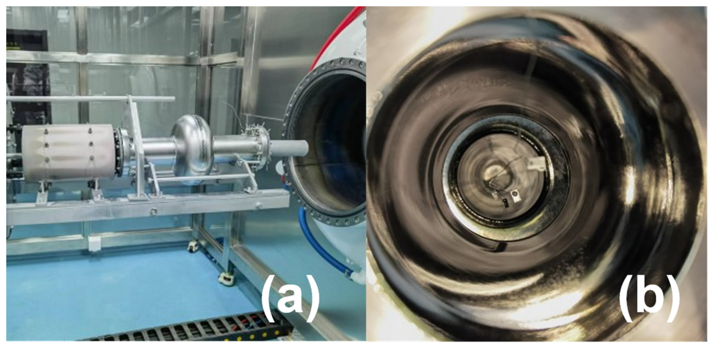
Figure 6.
Coating recipe used at SARI. The five different stages of the coating process are noted on the chart.
Figure 6.
Coating recipe used at SARI. The five different stages of the coating process are noted on the chart.
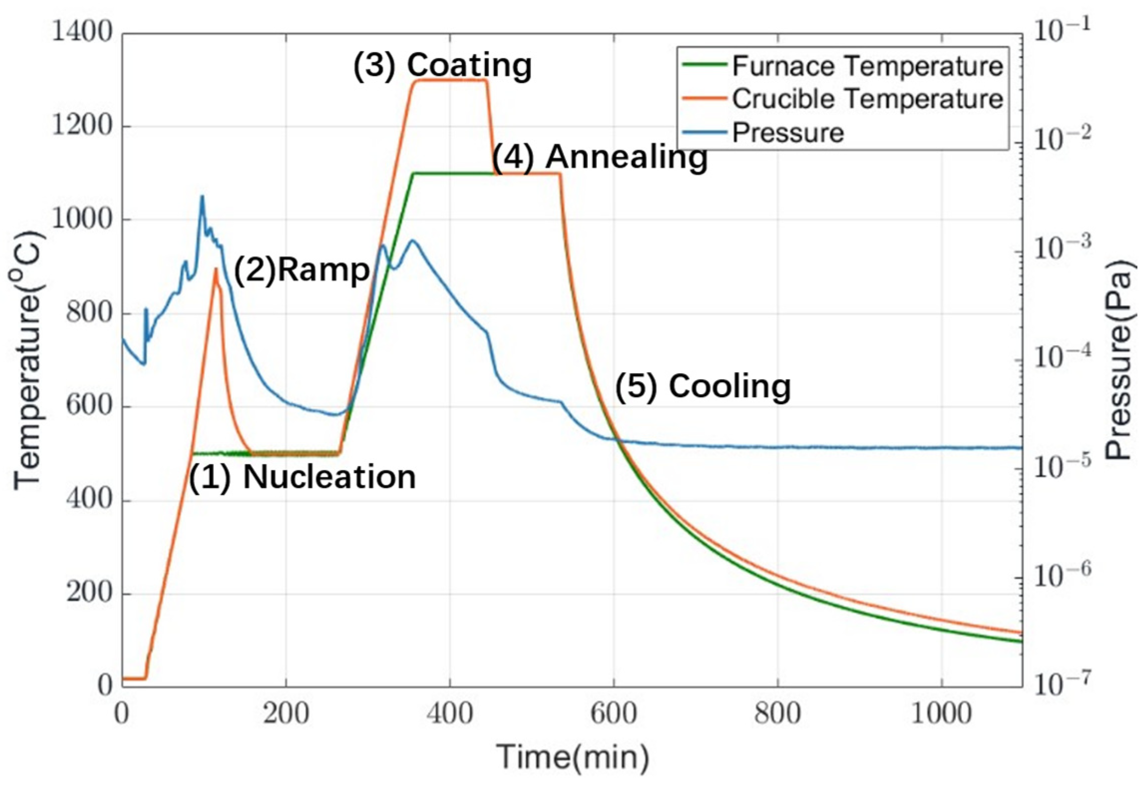
Figure 7.
(a) NF44n cavity before coating and (b,c) after coating.

Figure 8.
(a) Schematic of the sensors attached to the cavity and (b) actual picture.
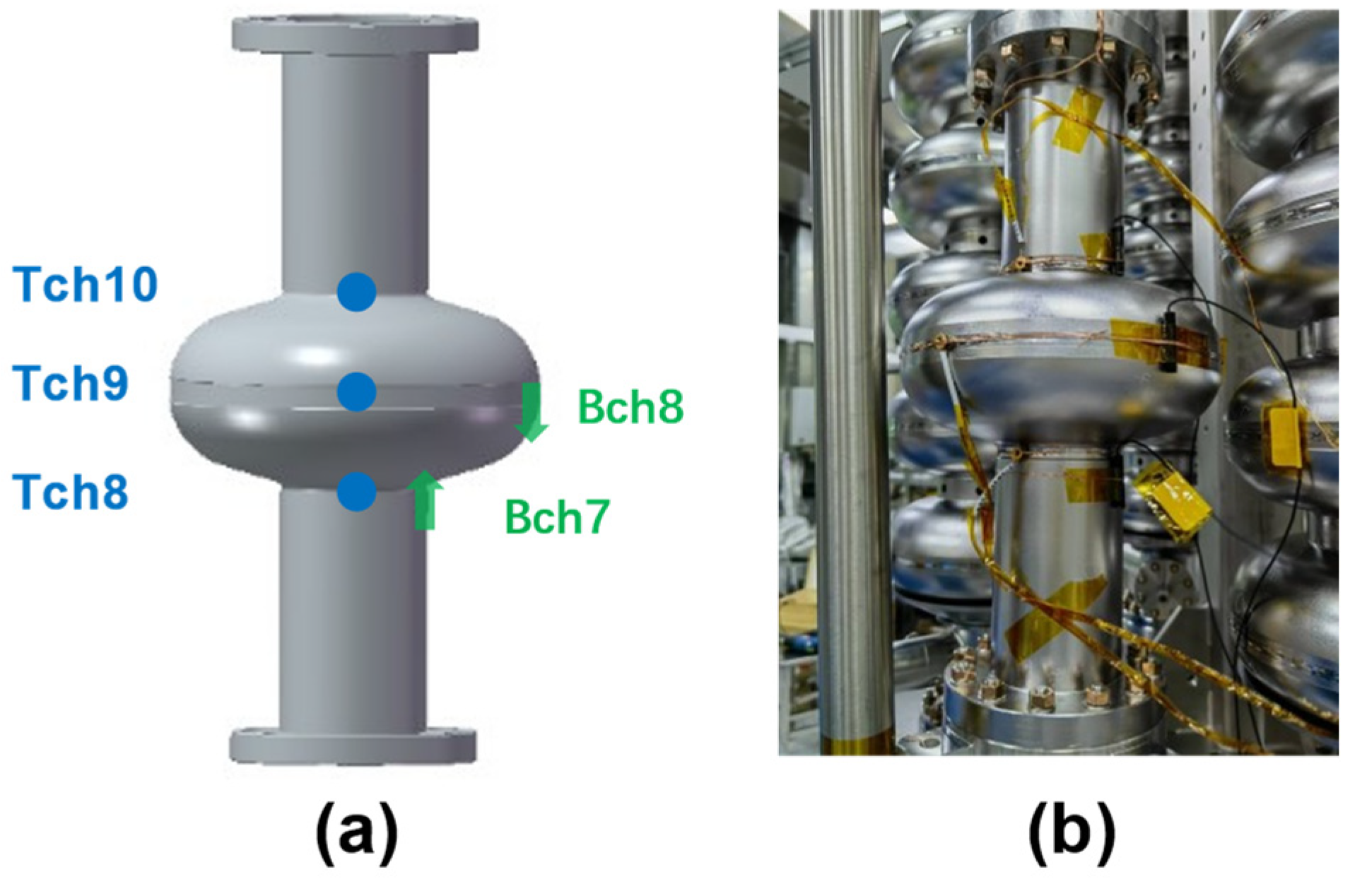
Figure 9.
Temperature and magnetic field curves versus time of NF44n passing through Nb3Sn critical temperature during the (a) faster and (b) slower periods of cooling.
Figure 9.
Temperature and magnetic field curves versus time of NF44n passing through Nb3Sn critical temperature during the (a) faster and (b) slower periods of cooling.

Figure 10.
NF44n coated cavity vertical tests after different cooling rates: quality factor and field emission radiation (µSv/h) versus accelerating gradients (MV/m) at 2 K and 4.2 K.
Figure 10.
NF44n coated cavity vertical tests after different cooling rates: quality factor and field emission radiation (µSv/h) versus accelerating gradients (MV/m) at 2 K and 4.2 K.

Figure 11.
Appearance of the samples before (left) and after (right) coating.

Figure 12.
SEM images of coated films show a range of Nb3Sn grains of around 2–3 µm (a), while the ion beam groove reveals a thickness of around 2 µm (b).
Figure 12.
SEM images of coated films show a range of Nb3Sn grains of around 2–3 µm (a), while the ion beam groove reveals a thickness of around 2 µm (b).

Figure 13.
Magnetization measurements of the Nb3Sn film during the cooling process with an external magnetic field of 10 Oe.
Figure 13.
Magnetization measurements of the Nb3Sn film during the cooling process with an external magnetic field of 10 Oe.

Figure 14.
(a) Spots near the equator of NF44n and (b) after annealing.

Figure 15.
(a) Sn in Nb foil and (b) NF45n after coating; (c) image of its equator.

Figure 16.
NF45ncoated cavity vertical tests: Quality factor and field emission radiation (µSv/h) versus accelerating gradients (MV/m) at 2 K and 4.2 K.
Figure 16.
NF45ncoated cavity vertical tests: Quality factor and field emission radiation (µSv/h) versus accelerating gradients (MV/m) at 2 K and 4.2 K.

Figure 17.
Thermal gradient near 18.3 K during faster and slower cooling.


Table 1.
Design parameters of the furnace used for Nb3Sn coating.
| Parameters | Furnace | Coating Chamber |
|---|---|---|
| Maximum temperature | ≥1300 °C | |
| Heating rate | ≥720 °C/h | |
| Temperature uniformity | <±4 °C | |
| Effective heating zone | Ø600 mm × 1000 mm | Ø300 mm × 600 mm |
| Target vacuum pressure | <8 × 10⁻⁵ Pa (25 °C) | <2 × 10⁻⁵ Pa (25 °C) |
| <2 × 10⁻³ Pa (1100 °C) | <3 × 10⁻⁴ Pa (1200 °C) | |
Table 2.
EDS composition of the Nb3Sn films after the coating process.
| Position | 1 | 2 | 3 |
|---|---|---|---|
| Sn content (at. %) | 25.90% | 25.69% | 25.98% |
| Average Sn content | 25.86% | ||
Disclaimer/Publisher’s Note: The statements, opinions and data contained in all publications are solely those of the individual author(s) and contributor(s) and not of MDPI and/or the editor(s). MDPI and/or the editor(s) disclaim responsibility for any injury to people or property resulting from any ideas, methods, instructions or products referred to in the content. |
© 2024 by the authors. Licensee MDPI, Basel, Switzerland. This article is an open access article distributed under the terms and conditions of the Creative Commons Attribution (CC BY) license (https://creativecommons.org/licenses/by/4.0/).
Share and Cite
MDPI and ACS Style
Chen, Q.; Zong, Y.; Wang, Z.; Xing, S.; Wu, J.; Dong, P.; Zhao, M.; Wu, X.; Rong, J.; Chen, J. First Results of Nb3Sn Coated Cavity by Vapor Diffusion Method at SARI. Coatings 2024, 14, 581. https://doi.org/10.3390/coatings14050581
AMA Style
Chen Q, Zong Y, Wang Z, Xing S, Wu J, Dong P, Zhao M, Wu X, Rong J, Chen J. First Results of Nb3Sn Coated Cavity by Vapor Diffusion Method at SARI. Coatings. 2024; 14(5):581. https://doi.org/10.3390/coatings14050581
Chicago/Turabian StyleChen, Qixin, Yue Zong, Zheng Wang, Shuai Xing, Jiani Wu, Pengcheng Dong, Miyimin Zhao, Xiaowei Wu, Jian Rong, and Jinfang Chen. 2024. "First Results of Nb3Sn Coated Cavity by Vapor Diffusion Method at SARI" Coatings 14, no. 5: 581. https://doi.org/10.3390/coatings14050581
Note that from the first issue of 2016, this journal uses article numbers instead of page numbers. See further details here.