
Formation of Organic Monolayers on KF-Etched Si Surfaces
School of Molecular and Life Sciences, Curtin University, Bentley, WA 6102, Australia
*
Author to whom correspondence should be addressed.
Surfaces 2024, 7(2), 358-368; https://doi.org/10.3390/surfaces7020022
Submission received: 5 March 2024
/
Revised: 30 April 2024
/
Accepted: 7 May 2024
/
Published: 10 May 2024
Abstract
:Silicon is the most commonly used material in the microelectronics industry, due to its inherent advantages of high natural abundance, low cost, and high purity, coupled with the chemical and electrical stability at the interface with its oxide. For molecular electronics applications, oxide-free Si surfaces are widely used because of the relative ease of removing the oxide (SiOx) by chemical means, yielding a surface which forms strong covalent bonds with a wide range of chemical functional groups; another advantage is that these surfaces remain oxide-free in the absence of oxidising agents. Standard procedures require the use of either HF, NH4F, or a mixture of both as the etching solution; however, these two chemicals are highly corrosive and toxic, posing a significant risk to the experimentalist. Here, we report that for silicon wafers etched by using potassium fluoride, a less toxic chemical, the resulting surface is free of oxides and can be functionalized by self-assembled monolayers of 1,8-nonadiyne. To demonstrate this, Si/SiOx wafers were etched by using either KF or NH4F, followed by hydrosilylation with 1,8-nonadiyne and a click reaction of the terminal alkyne with azidomethylferrocene. The surface coverages and electron transfer kinetics of the ferrocene-terminated KF-etched surfaces are comparable to those formed by acidic fluoride etching procedures. This is the first study comparing the differences between surfaces functionalized by self-assembled monolayers of 1,8-nonadiyne which were etched by KF and NH4F. KF could be used as a replacement chemical for etching silicon wafers when a less corrosive and toxic chemical is required.

1. Introduction
Silicon is the second most abundant element on earth, resulting in low costs, along with high purity and high chemical and electrical stability of the interface with its oxide. This makes it an excellent semiconducting material for electrode fabrication for Li-ion batteries and explains its abundance in the microelectronics industry. Si has been used for applications in various devices, for example, in electrical biosensors and photovoltaics. To modify a Si/SiOx surface, there are two methods: The first one is the direct functionalization of SiOx, by silanisation or tethering by aggregation and growth. The second one, which is more common, is by removal of the oxide layer, then covalent attachment of organic layers to the oxide-free Si. Oxide-free silicon is preferred due to the increased functionalization possibilities (alkenes, alkynes, alcohol, and thiols) compared with oxidized silicon (organo-silanes) and the improved electrical characteristics, due to the removal of a thin dielectric layer of oxide [1,2,3,4,5,6,7,8,9,10].
Previously, methods for etching silicon wafers from SiOx to Si–H have used NH4F or HF [11,12,13,14,15,16,17,18]. However, both of these chemicals are strongly corrosive and highly toxic due to their acidic nature. Thus, attention has shifted toward etching in solutions that are safer and more environmentally conscious. Dilute HF is another alternative method for etching silicon wafers from SiOx to Si–H [19,20]. The dilution varies but is often used as 200:1 or 500:1 HF:H2O, owing to the advantages of reduced corrosiveness, lower volatility, and lower reactivity. These diluted HF solutions are a better method for etching silicon wafers, affording a greater etching rate when compared with the concentrated HF solutions. The etching rate is reported to be twice as fast for dilute HF solutions compared with the stock high-concentration HF solutions [21]. However, the dilution process requires the treatment and handling of concentrated HF; thus, it is still a highly dangerous operation. Even once diluted, the waste liquid still has adverse effects on local environments, for example, water bodies, soil, and aquatic organisms. In 2005, Adachi et al. demonstrated that aqueous KF solutions are of equal quality to HF and NH4F in producing Si–H [22] and remove oxide on the surface at a reasonable rate. Their KF-treated surfaces showed hydrophobicity after immersion in aqueous KF (5 M) for 30 min. However, the formation of covalently linked organic layers after the oxide has been removed by KF has not yet been studied. Although there are several papers about KF and NH4F etching, there is no work on utilizing KF etching to form organic monolayers on silicon and studying the electron properties.
Upon contact with water or moist skin, ammonium fluoride (NH4F) converts into hydrogen fluoride, meaning that these two chemicals should be handled with equivalent care and precautions. Potassium fluoride (KF) also hydrolyses in water but to a lesser extent than NH4F and thus produces less of the highly toxic HF. Seeing as the fluoride component is necessary for etching silicon wafers to obtain oxide-free silicon wafers, it makes sense to want a method which provides the lowest risk or danger to the experimentalist. For treating any fluoride spillage on the skin, calcium gluconate gels (2.5% w/v) are recommended following copious rinsing in water (15 min under running water). For example, in our laboratory, a tube of calcium gluconate gel is stored within reach of the fume hood, below room temperature, and is routinely replaced before the expiry date. The calcium in these gels serves the purpose of neutralizing any free fluoride anions (F−), preventing them from further reacting with the patient’s body. While these safety precautions would not change when using KF over either HF or NH4F, the immediate dangers associated with them are mitigated. When using a small amount of fluoride salts, either KF or NH4F, the KF solution is less corrosive and causes less immediate damage to tissues upon contact with the skin or eyes compared with both NH4F and HF [22,23,24,25,26,27]. In terms of pH, KF is slightly basic but closer to neutral than the more acidic HF or NH4F solutions which are commonly used. Therefore, KF is less toxic and safer to handle than NH4F and HF [28,29].
In this article, we test whether surfaces etched by KF can be used to attach a monolayer via a hydrosilylation reaction. This monolayer can be labelled by a redox active species (ferrocene) and then characterized electrochemically regarding surface coverage and their electrochemical rate constants. KF could serve as the etching solution for silicon wafers when less toxic chemicals are needed. For this purpose, the silicon wafers were etched by either solution and then functionalised by 1,8-nonadiyne via a hydrosilylation reaction, followed by a click reaction of the terminal alkyne with azidomethylferrocene; a scheme showing oxide removal and the associated monolayer functionalization is shown in Figure 1 [30,31,32,33,34,35,36]. Cyclic voltammetry (CV) was used to study the ferrocene surface coverages, and electrochemical impedance spectroscopy (EIS) allowed for the determination of electron transfer kinetics (ket). Water contact angle measurements evaluated the efficacy of the KF etching method compared with the standard NH4F method, and X-ray photoelectron spectroscopy (XPS) was used to characterize the chemical methods for removing the oxide layers (KF against NH4F). The surface topography, roughness, and presence of characteristic Si(111) terraces were monitored by atomic force microscopy (AFM).
2. Materials and Methods
2.1. Materials
All chemicals were purchased at analytical grade and used as received, unless otherwise specified below. Preparation of aqueous solutions, and surface and glassware cleaning were performed by using Milli–Q water (>18 MΩ cm). Dichloromethane (DCM)) (Honeywell; Charlotte, NC, USA, >99.9%) and 2–propanol (RCI Labscan, Bangkok, Thailand) were re-distilled prior to use. The cleaning and etching of the silicon wafers used hydrogen peroxide (H2O2; Honeywell; Charlotte, NC, USA, 30 wt% in water), sulfuric acid (H2SO4; Sigma-Aldrich; Melbourne, Australia, 95–97%, Puranal TM), ammonium fluoride (NH4F; Sigma-Aldrich; Melbourne, Australia, Puranal TM), and potassium fluoride (KF; Sigma-Aldrich; Melbourne, Australia, 40 wt% in water), with each being of semiconductor grade. 1,8–Nonadiyne (98%) was purchased from Sigma-Aldrich (Melbourne, Australia) and used without further purification. Azidomethylferrocene was synthesised from ferrocene methanol by using a procedure from the literature [37]. The chemicals involved in the synthesis were ferrocene methanol (Sigma-Aldrich; Melbourne, Australia, 97%), glacial acetic acid (Sigma-Aldrich; Melbourne, Australia, ≥99%), sodium azide (Sigma-Aldrich; Melbourne, Australia, ≥99.5%), sodium bicarbonate (Sigma-Aldrich; Melbourne, Australia, ≥95%), hexane (Heneywell; Charlotte, NC, USA, HPLC grade), ethyl acetate (Heneywell; Charlotte, NC, USA, HPLC grade), and silica (Silicycle; Quebec, QC, Canada, 230–400 mesh). All of the electrochemical experiments used aqueous perchloric acid (1.0 M) (Sigma-Aldrich; Melbourne, Australia, 70%) as the electrolyte solution. Our silicon wafers were purchased from Siltronix, S.A.S. (Archamps, France), and were p-type boron-doped (111), with a thickness of 500 ± 25 μm and a resistivity of 0.007–0.013 Ω cm.
2.2. Surface Modification
2.2.1. Silicon Preparation
The method for hydrosilylation of 1,8-nonadiyne with Si–H has previously been reported in the literature [11,37,38]. In summary, a silicon wafer is cut into smaller pieces (approx. 1 × 1 cm2) followed by sequential washes in DCM, 2-propanol, and water. The surfaces are then submerged in hot piranha solution (130 °C; 3:1 (v/v) mixture of sulfuric acid (95–97%) to hydrogen peroxide (30%)) for 30 min, rinsed in copious amounts of water before etching in either ammonium fluoride or potassium fluoride for 13 min (ambient conditions (21 °C and 30% relative humidity)) which has been deoxygenated under a stream of argon for 15 min. At this point, the surface is an oxide-free, hydrogen-terminated Si surface [14,39]. These etched samples were quickly rinsed with Milli–Q water and DCM before being stored for short periods of time (less than 15 min) in a deoxygenated sample of 1,8–nonadiyne. These surfaces were quickly transferred into an isolated reaction chamber maintained under continuous nitrogen flow and illuminated with UV light (Vilber; VL–215.M, λ = 312 nm) for two hours.
2.2.2. Copper-Catalysed Azide–Alkyne “Click” Reaction
Azidomethylferrocene was reacted with the terminal alkyne group of the SAMs in S–2 via a copper-catalysed click reaction. In summary, samples of S–2 were incubated in a mixture of 0.4 mM copper (II) sulphate pentahydrate, sodium ascorbate (5 mg/mL), and 0.5 mM azidomethylferrocene. The reaction was carried out in the dark for 120 min at room temperature and pressure. The Si electrodes were removed from the Cu-AAC solution and were washed sequentially by using 2–propanol, Milli-Q water, 0.5 M hydrochloric acid, Milli–Q water, 2–propanol, and DCM. Finally, these Si electrodes (now S–3) were blown-dry under a stream of argon before analysis.
2.3. Surface Characterization
2.3.1. Electrochemical Measurements
All our electrochemical measurements were undertaken by using a single-compartment, three-electrode PTFE cell connected to a CHI650 electrochemical workstation (CH Instruments, Austin, TX, USA). For the three-electrode setup, a modified silicon surface was used as the working electrode, a platinum wire as the auxiliary (counter) electrode, and an aqueous Ag/AgCl electrode (1.0 M KCl; CH Instruments, Austin, TX, USA) as the reference electrode. In all electrochemical measurements, an aqueous 1.0 M perchloric acid solution was used as the electrolyte. A gallium–indium eutectic was rapidly spread on the backside of the silicon wafer and contacted to a copper plate. CV was used for electrochemical characterisation and determination of the half-wave potential (E1/2), which was used for EIS, where the half wave potential is equal to the DC offset [40,41,42]. For the EIS measurements, the AC amplitude was set to 15 mV, with frequency scanning between 1 and 100,000 Hz. The EIS data were fitted to an equivalent Randles circuit, which is shown in Figure S2. ket was calculated according to the following equation: (Cads)eff = Q 1/α Re (1−α)/α, where Re is the total resistance, and Q and α represent global properties. Q represents the differential capacitance of the interface in the case where α = 1, and the rate constant is determined by the following equation: , where ket is the rate constant, Ret is the electron transfer resistance, and (Cads)eff is the effective pseudocapacitance [43]. The ferrocene surface coverages (Γ) can be used to estimate the molecular surface coverage based upon the oxidation and reduction signals observed in the CV. The charge (Q) is approximated by integration of the oxidation and reduction signals, and surface coverage is determined according to Γ = Q/nFA (where Q is the charge, n is the number of electrons involved in the redox reaction, F is Faraday’s constant (96,485 C/mol), and A is the electrode area).
2.3.2. Static Water Contact Angle Analysis
Static water contact angles were utilized for determining the wettability of our etched silicon substrates. They were measured by using an automatic Krüss DSA 100 goniometer (Hamburg, Germany), and the recorded values were reported to the nearest whole number. The values reported in this manuscript are the average values of at least three different surfaces. The reported error values represent the standard deviation of at least three different droplets on three different substrates.
2.3.3. Atomic Force Microscopy (AFM)
AFM was used to characterise the surface topography and roughness and to monitor for the presence of persistent surface oxidation following the different etching methods. For this, all images were captured with a Bruker Dimension FastScan atomic force microscope (Billerica, MA, USA) in air at standard room temperature and pressure. Nanoscope Analysis software (Version 1.90) was used for all AFM topography image processing and roughness analysis. For the topography imaging antimony (n)-doped silicon AFM probes (TESPA-V2; Bruker AFM probes) were used, with a spring constant of 42 Nm−1 and a resonant frequency of 320 kHz. All measurements were undertaken in air by using tapping mode, an image size of 25 µm2 at a resolution of 256 points/line, and the scan rate of 1.0 Hz.
2.3.4. X-ray Photoelectron Spectroscopy (XPS)
X-ray photoelectron spectroscopy (XPS) analysis of the etched silicon substrates was performed by using a Kratos Axis Ultra DLD fitted with an Al Kα (hυ1486.6 eV) monochromatic radiation source functioning at 225 W. The hemispherical analyser (165 mm in radius) was run in fixed analysed transmission mode. The chamber was set to operate at 2 × 10⁻⁵ Torr with the photoelectron take-off angle set up normal to the sample surface. We analysed a sample area of 300 × 700 µm, using an internally fixed flood gun to mitigate the effects of surface charging. Given the relative simplicity of our surfaces, the survey spectra (averaged among three scans) were acquired in the range of 0 to 1100 eV, a dwell time of 55 ms, step size of 0.5 eV, and a pass energy set to 160 eV. For the high-resolution scans (accumulation of 10 scans, for Si 2p and O 1s regions), we used a pass energy of 20 eV and lower step sizes, specifically 0.05 eV (Si 2p, 90–110 eV) or 0.1 eV (O 1s, 520–540 eV). All of our XPS data were processed and fitted by using CasaXPS (version 2.3.18).
3. Results
3.1. Contact Angle
We analysed the bare etched surfaces firstly by using the water contact angle to detect differences in the wettability of the Si–H surfaces depending on the preparation method.
This can offer insights into the Si–H surface coverage and also into how efficiently the oxide layer has been removed (since Si–OH is hydrophilic and Si–H is hydrophobic). This can also be used to characterise the uniformity of the Si–H layer, since each location should show similar wettability values if a uniform layer of Si–H is formed, resulting in low error values. Figure 2a–c show annotated images of the water contact angles along with their associated error values. From this, we see that the surface etched in NH4F has a greater contact angle, indicating greater hydrophobicity (82 ± 5°), while the surface etched by KF shows a slightly lower average contact angle (75 ± 6°). While this is true, these values fall within the error values of one another, and the difference could be due to some randomness associated with the technique. Another more likely explanation is that this slight difference is caused by the greater surface roughness of the KF-etched surface when compared with the flatter and more uniform NH4F surface. (See Section 3.2.)
3.2. Atomic Force Microscopy (AFM)
We took these oxide-free silicon surfaces and performed AFM topography imaging. These images are presented in Figure 2d,e, which clearly show the presence of flat terraces (characteristic of Si(111) substrates) with smooth edges all across the silicon surface.
Visually, the surfaces appear similar to Figure 2d (etched in NH4F), showing more clearly the fine topography details due to fewer high regions across the image. However, when we observe the straight-line height profiles (along the white dotted lines and the inset in the top right corner), it can be seen how the height variation is minimal (less than 1–2 nm across either surface) across both the NH4F- and KF-etched surfaces. The root mean square roughness (RMS) for the NH4F-etched surface is 0.294 nm, while for the KF-etched surface, it is 0.517 nm. The roughness is within the range of standard hydrogen-terminated silicon surfaces [44,45] while still highlighting that the surfaces etched by KF are rougher than those etched in NH4F. This would allow for the explanation of the difference in water contact angles observed in Figure 2c and discussed in Section 3.1. On a rougher substrate, the water droplet is likely to deform slightly and become exposed to regions of low Si–H coverage. This would in turn result in a lower angle recorded by static water contact angle measurements.
3.3. X-ray Photoelectron Spectroscopy (XPS)
We performed XPS characterisation on a bare surface etched by using either NH4F or KF; our XPS spectra show the expected Si 2p signals from S–1 which were etched in NH4F or KF (Figure 3a,b). Figure 3a shows the XPS Si 2p narrow scan for a Si–H surface which was etched by NH4F. The Si 2p high-resolution spectrum was fitted by using two peaks, with the main emission from 98–101 eV being composed of one spin–orbit split with two peaks at 98.85 eV and 99.45 eV, corresponding to the low- and high-energy spins of the Si 2p3/2 and Si 2p1/2 orbitals, respectively. Of note, there is a lack of a SiOx signal (which would appear at approximately 102–103 eV), indicating that the oxide layer was removed by using the KF etching procedure. Figure 3b shows the XPS Si 2p narrow scan for a Si–H surface which was etched by KF; this shows the same Si 2p signals for the spin–orbit splitting, but it does show limited amounts of SiOx at 102.5 eV (1.7%). The corresponding survey XPS spectra for S–1 and high-resolution O 1s spectra are included in Figure 3c,d and Figure S1 (Supplementary Materials). In the O1s high-resolution spectrum, we observe only one peak in the region 530–536 eV, due to the presence of residual oxygen in the instrument itself, indicating that negligible amounts of oxide are present for surfaces etched in either NH4F or KF.
3.4. Electrochemical Studies
The key purpose of this work is to compare the electrochemical properties of surfaces etched by using either conventional methods (NH4F) or the newer, safer method (KF). Thus, we functionalised both surfaces by using a common redox moiety (ferrocene), by a copper-catalysed click reaction, as shown in Figure 1. By using this functionalisation, we probed the coverages and electron transfer kinetics by cyclic voltammetry and electrochemical impedance spectroscopy, respectively. We observe a small peak separation (24 mV) in the oxidation and reduction signals of Figure 4a (etched in NH4F). In comparison, the oxidation and reduction signals for Figure 4b (etched in KF) show a larger separation (78 mV), often indicating a slower electron transfer mechanism, which could be caused by a less uniform or less dense monolayer array. This occurs due to a decreased electron density in the monolayer structure, meaning electron transfer becomes more difficult and sees a decrease in the electron transfer rates, characterized by the hysteresis of the oxidation and reduction signals [11]. To understand this further, the surface coverages of the ferrocene moieties were calculated from the oxidation signals in the CV (by using the equation presented in Section 2.3.1). The surface coverage was determined to be (1.11 ± 0.23) × 1014 ferrocene cm−2 and (7.83 ± 2.24) × 1013 ferrocene cm−2 for the NH4F-etched and KF-etched surfaces, respectively. (Figure 4c) This would indicate that more dense monolayers with better packing are produced on NH4F-etched surfaces and thus should show faster electron transfer kinetics as a result.
To assess the charge transfer kinetics, electrochemical impedance spectroscopy (EIS) was performed on S–3. The electron transfer kinetics (ket) values were (634.18 ± 9.59) s−1 and (354.26 ± 14.4) s−1 for the NH4F-etched surface and KF-etched surface, respectively (Figure 5a–d). This confirms that electron transfer occurs faster on NH4F surfaces. This would mean that these KF-etched surfaces could be used as an alternative for those without the appropriate funds or facilities to use NH4F without greatly sacrificing the quality of their electrochemical results. The equivalent circuit used to fit the EIS data is shown in Figure S2 (Supplementary Materials). The Nyquist and the Bode plots in Figure 5a–c visually indicate that the resistance of the monolayer on the KF-etched surface is higher than that on the NH4F-etched surface. The diameter of the semicircle on the real component of the impedance on the KF-etched surface is bigger than that on the NH4F-etched surface (x-axis in Figure 5a,b). This reflects that the resistance resulting from monolayer formation is greater for the KF-etched surfaces than the NH4F surfaces. The Bode plots are shown in Figure 5c and allow for a rapid visualization of the kinetic characteristics of our modified electrode systems. When the AC frequency approaches the time constant of the reaction, the phase angle value decreases and eventually reaches the minimum value. By using this phase angle minimum and the corresponding frequency, you can predict the different electron transfer kinetic speeds of the two systems. A phase angle minimum occurring at higher frequency indicates a faster electron transfer rate. On the contrary, a phase angle minimum occurring at lower frequency means a slower electron transfer rate. From our Bode plots result (Figure 5c), the phase angle minimum of the NH4F-etched surface occurs at higher frequency than that of the KF-etched surface, which means that the resistance resulting from the surface and monolayer formation on the NH4F-etched surface is lower compared with the KF-etched surface. This also indicates that the electron transfer kinetics should be faster on our NH4F-etched surfaces than on the KF-etched surfaces, which is confirmed by the fitting and subsequent calculation of the ket values presented in Figure 5d and discussed above. Although the ket on KF-etched surfaces is only half of that on the NH4F-etched surfaces, this slower electron transfer kinetics will not deter the use of KF-etched surfaces for electrochemical studies, as the signal is sufficient to be used for monitoring changes in electron transfer upon, for example, interaction with analytes for chemical sensors and bio-sensing devices.
4. Conclusions
In summary, we demonstrate that KF etches the oxide layer from Si, resulting in Si–H layers, which are then subsequently used for a hydrosilylation reaction and the formation of covalently linked organic monolayers. The density of the molecular films formed on KF-etched Si surfaces is lower but comparable to that of those formed on NH4F-etched Si surfaces. A slightly higher surface roughness is observed for the KF-etched Si surfaces compared with the NH4F-etched Si surfaces, but this roughness is not a roadblock in forming molecular films of good quality. Despite the electron transfer rate constant, the ket of the KF-etched surfaces is half of that of the NH4F-etched surfaces, which is sufficient for utilising KF-etched surfaces for fundamental electrochemical studies and electrochemical devices utilising molecular films on silicon.
KF-etched Si surfaces provide an opportunity for functionalising silicon wafers in a more accessible way, by using a less corrosive and toxic chemical. This could allow smaller laboratories, which may be ill equipped to handle other more dangerous fluoride-containing chemicals, to covalently functionalise oxide-free silicon electrodes, study fundamental SAM systems, and develop electrochemical devices such as biosensors [46].
Supplementary Materials
The following supporting information can be downloaded at: https://www.mdpi.com/article/10.3390/surfaces7020022/s1, Figure S1: XPS survey spectra, Figure S2: Randles circuit used to fit the EIS data, Table S1: Original EIS data.
Author Contributions
N.D. conceived the idea and supervised the research. T.L. performed the electrochemical measurements, AFM measurements, contact angle measurements, and XPS measurements. Z.D. helped in writing the manuscript. All authors contributed to the interpretation of the data. All authors have read and agreed to the published version of the manuscript.
Funding
N.D. acknowledges support from the Western Australian Future Health Research and Innovation Fund.
Institutional Review Board Statement
Not applicable.
Informed Consent Statement
Not applicable.
Data Availability Statement
The experimental data are available from the corresponding author upon reasonable request.
Conflicts of Interest
The authors declare no conflicts of interest.
References
- Peiris, C.R.; Ferrie, S.; Ciampi, S.; Rickard, W.D.; Darwish, N. Memristor arrays formed by reversible formation and breakdown of nanoscale silica layers on Si–H surfaces. ACS Appl. Nano Mater. 2022, 5, 6609–6617. [Google Scholar] [CrossRef]
- Fritz, P.A.; Lange, S.C.; Giesbers, M.; Zuilhof, H.; Boom, R.M.; Schroën, C. Simultaneous silicon oxide growth and electrophoretic deposition of graphene oxide. Langmuir 2019, 35, 3717–3723. [Google Scholar] [CrossRef] [PubMed]
- Van den Boom, A.F.; Ferro, S.; Gelvez-Rueda, M.; Zuilhof, H.; Ehrler, B. Toward Improving Triplet Energy Transfer from Tetracene to Silicon Using a Covalently Bound Tetracene Seed Layer. J. Phys. Chem. Lett. 2023, 14, 4454–4461. [Google Scholar] [CrossRef] [PubMed]
- Kumar, R.; Yan, H.; McCreery, R.L.; Bergren, A.J. Electron-beam evaporated silicon as a top contact for molecular electronic device fabrication. Phys. Chem. Chem. Phys. 2011, 13, 14318–14324. [Google Scholar] [CrossRef] [PubMed]
- Ru, J.; Szeto, B.; Bonifas, A.; McCreery, R.L. Microfabrication and integration of diazonium-based aromatic molecular junctions. ACS Appl. Mater. Interfaces 2010, 2, 3693–3701. [Google Scholar] [CrossRef] [PubMed]
- Mooste, M.; Kibena-Põldsepp, E.; Ossonon, B.D.; Bélanger, D.; Tammeveski, K. Oxygen reduction on graphene sheets functionalised by anthraquinone diazonium compound during electrochemical exfoliation of graphite. Electrochim. Acta 2018, 267, 246–254. [Google Scholar] [CrossRef]
- De Villeneuve, C.H.; Pinson, J.; Bernard, M.; Allongue, P. Electrochemical formation of close-packed phenyl layers on Si (111). J. Phys. Chem. B 1997, 101, 2415–2420. [Google Scholar] [CrossRef]
- Hetemi, D.; Pinson, J. Surface functionalisation of polymers. Chem. Soc. Rev. 2017, 46, 5701–5713. [Google Scholar] [CrossRef]
- Hetemi, D.; Noël, V.; Pinson, J. Grafting of diazonium salts on surfaces: Application to biosensors. Biosensors 2020, 10, 4. [Google Scholar] [CrossRef]
- Ha, T.Q.; Planje, I.J.; White, J.R.; Aragones, A.C.; Díez-Pérez, I. Charge transport at the protein–electrode interface in the emerging field of BioMolecular Electronics. Curr. Opin. Electrochem. 2021, 28, 100734. [Google Scholar] [CrossRef]
- Li, T.; Dief, E.M.; Lyu, X.; Rahpeima, S.; Ciampi, S.; Darwish, N. Nanoscale silicon oxide reduces electron transfer kinetics of surface-bound ferrocene monolayers on silicon. J. Phys. Chem. C 2021, 125, 27763–27770. [Google Scholar] [CrossRef]
- Henry-de-Villeneuve, C.; Nguyen-Le, T.L.; Ozanam, F.; Allongue, P. Structure of Mixed Acid/Decyl Monolayers Grafted on Oxide-Free Si (111) Surfaces. Langmuir 2019, 35, 2547–2553. [Google Scholar] [CrossRef] [PubMed]
- Fabre, B.; Hauquier, F. Boronic acid-functionalized oxide-free silicon surfaces for the electrochemical sensing of dopamine. Langmuir 2017, 33, 8693–8699. [Google Scholar] [CrossRef] [PubMed]
- Peiris, C.R.; Vogel, Y.B.; Le Brun, A.P.; Aragonès, A.C.; Coote, M.L.; Díez-Pérez, I.; Ciampi, S.; Darwish, N. Metal–single-molecule–semiconductor junctions formed by a radical reaction bridging gold and silicon electrodes. J. Am. Chem. Soc. 2019, 141, 14788–14797. [Google Scholar] [CrossRef] [PubMed]
- Allongue, P.; Kieling, V.; Gerischer, H. Etching mechanism and atomic structure of H-Si (111) surfaces prepared in NH4F. Electrochim. Acta 1995, 40, 1353–1360. [Google Scholar] [CrossRef]
- Frank, C.J.; McCreery, R.L.; Redd, D.C.; Gansler, T.S. Detection of silicone in lymph node biopsy specimens by near-infrared Raman spectroscopy. Appl. Spectrosc. 1993, 47, 387–390. [Google Scholar] [CrossRef]
- Dasog, M.; Kehrle, J.; Rieger, B.; Veinot, J.G. Silicon nanocrystals and silicon-polymer hybrids: Synthesis, surface engineering, and applications. Angew. Chem. Int. Ed. 2016, 55, 2322–2339. [Google Scholar] [CrossRef] [PubMed]
- Aragonès, A.C.; Martín-Rodríguez, A.; Aravena, D.; Puigmartí-Luis, J.; Amabilino, D.B.; Aliaga-Alcalde, N.; González-Campo, A.; Ruiz, E.; Díez-Pérez, I. Tuning Single-Molecule Conductance in Metalloporphyrin-Based Wires via Supramolecular Interactions. Angew. Chem. Int. Ed. 2020, 132, 19355–19363. [Google Scholar] [CrossRef]
- Tong, Q.-Y.; Gan, Q.; Fountain, G.; Hudson, G.; Enquist, P. Low-temperature bonding of silicon-oxide-covered wafers using diluted HF etching. Appl. Phys. Lett. 2004, 85, 2762–2764. [Google Scholar] [CrossRef]
- Tsuboi, T.; Sakka, T.; Ogata, Y.H. Chemical etching of porous silicon in diluted hydrofluoric acid. Solid State Commun. 1998, 109, 195–199. [Google Scholar] [CrossRef]
- Hu, S.M.; Kerr, D.R. Observation of Etching of n-Type Silicon in Aqueous HF Solutions. J. Electrochem. Soc. 1967, 114, 414. [Google Scholar] [CrossRef]
- Noguchi, H.; Adachi, S. Chemical treatment effects of silicon surfaces in aqueous KF solution. Appl. Surf. Sci. 2005, 246, 139–148. [Google Scholar] [CrossRef]
- Machavaram, V.; Badcock, R.; Fernando, G. Fabrication of intrinsic fibre Fabry–Perot sensors in silica fibres using hydrofluoric acid etching. Sens. Actuators A Phys. 2007, 138, 248–260. [Google Scholar] [CrossRef]
- Tomioka, K.; Adachi, S. Strong and stable ultraviolet emission from porous silicon prepared by photoetching in aqueous KF solution. Appl. Phys. Lett. 2005, 87, 251920. [Google Scholar] [CrossRef]
- Seo, Y.H.; Nahm, K.S.; Lee, K.B. Mechanistic Study of Silicon Etching in HF-KBrO3-H2O Solution. J. Electrochem. Soc. 1993, 140, 1453. [Google Scholar] [CrossRef]
- Takai, C.; Ishino, T.; Fuji, M.; Shirai, T. Rapid and high yield synthesis of hollow silica nanoparticles using an NH4F catalyst. Colloids Surf. A Physicochem. Eng. Asp. 2014, 446, 46–49. [Google Scholar] [CrossRef]
- Suratwala, T.I.; Miller, P.E.; Bude, J.D.; Steele, W.A.; Shen, N.; Monticelli, M.V.; Feit, M.D.; Laurence, T.A.; Norton, M.A.; Carr, C.W. HF-based etching processes for improving laser damage resistance of fused silica optical surfaces. J. Am. Ceram. Soc. 2011, 94, 416–428. [Google Scholar] [CrossRef]
- Tomita, N.; Adachi, S. Chemical treatment effects on Si (111) surfaces in aqueous NaF solution. Jpn. J. Appl. Phys. 2001, 40, 6705. [Google Scholar] [CrossRef]
- Sun, L.; Shao, T.; Zhou, X.; Li, F.; Chen, S.; Li, W.; Ye, X.; Huang, J.; Li, B.; Yang, L. KOH-based shallow etching for exposing subsurface damage and increasing laser damage resistance of fused silica optical surface. Opt. Mater. 2020, 108, 110249. [Google Scholar] [CrossRef]
- Scarpetta-Pizo, L.; Venegas, R.; Barrias, P.; Muñoz-Becerra, K.; Vilches-Labbé, N.; Mura, F.; Méndez-Torres, A.M.; Ramírez-Tagle, R.; Toro-Labbé, A.; Hevia, S. Electron Spin-Dependent Electrocatalysis for the Oxygen Reduction Reaction in a Chiro-Self-Assembled Iron Phthalocyanine Device. Angew. Chem. Int. Ed. 2023, 136, e202315146. [Google Scholar] [CrossRef]
- Li, T.; Dief, E.M.; Kalužná, Z.; MacGregor, M.; Foroutan-Nejad, C.; Darwish, N. On-Surface Azide–Alkyne Cycloaddition Reaction: Does It Click with Ruthenium Catalysts? Langmuir 2022, 38, 5532–5541. [Google Scholar] [CrossRef] [PubMed]
- Li, T.; Peiris, C.R.; Aragonès, A.C.; Hurtado, C.; Kicic, A.; Ciampi, S.; MacGregor, M.; Darwish, T.; Darwish, N. Terminal Deuterium Atoms Protect Silicon from Oxidation. ACS Appl. Mater. Interfaces 2023, 15, 47833–47844. [Google Scholar] [CrossRef] [PubMed]
- Mahmoud, A.M.; Bergren, A.J.; McCreery, R.L. Derivatization of optically transparent materials with diazonium reagents for spectroscopy of buried interfaces. Anal. Chem. 2009, 81, 6972–6980. [Google Scholar] [CrossRef] [PubMed]
- Bentley, C.L.; Kang, M.; Unwin, P.R. Time-resolved detection of surface oxide formation at individual gold nanoparticles: Role in electrocatalysis and new approach for sizing by electrochemical impacts. J. Am. Chem. Soc. 2016, 138, 12755–12758. [Google Scholar] [CrossRef] [PubMed]
- Escobar, G.; Venegas, R.; Ponce, I.; Toro-Labbé, A.; Zagal, J.H.; Recio, F.J.; Muñoz-Becerra, K. Elucidating the electronic synergetic effects in heteroatomic doped FeN4-CNR (R=-F,-Cl,-Br) oxygen reduction catalysts. Electrochim. Acta 2023, 466, 143060. [Google Scholar] [CrossRef]
- Veerbeek, J.; Steen, R.; Vijselaar, W.; Rurup, W.F.; Korom, S.A.; Rozzi, A.; Corradini, R.; Segerink, L.; Huskens, J. Selective functionalization with PNA of silicon nanowires on silicon oxide substrates. Langmuir 2018, 34, 11395–11404. [Google Scholar] [CrossRef]
- Ciampi, S.; Eggers, P.K.; Le Saux, G.; James, M.; Harper, J.B.; Gooding, J.J. Silicon (100) electrodes resistant to oxidation in aqueous solutions: An unexpected benefit of surface acetylene moieties. Langmuir 2009, 25, 2530–2539. [Google Scholar] [CrossRef]
- Ciampi, S.; Böcking, T.; Kilian, K.A.; James, M.; Harper, J.B.; Gooding, J.J. Functionalization of acetylene-terminated monolayers on Si (100) surfaces: A click chemistry approach. Langmuir 2007, 23, 9320–9329. [Google Scholar] [CrossRef] [PubMed]
- Golvari, P.; Alkameh, K.; Kuebler, S.M. Si–H surface groups inhibit methacrylic polymerization: Thermal hydrosilylation of allyl methacrylate with silicon nanoparticles. Langmuir 2022, 38, 8366–8373. [Google Scholar] [CrossRef]
- Darwish, N.; Eggers, P.K.; Ciampi, S.; Tong, Y.; Ye, S.; Paddon-Row, M.N.; Gooding, J.J. Probing the effect of the solution environment around redox-active moieties using rigid anthraquinone terminated molecular rulers. J. Am. Chem. Soc. 2012, 134, 18401–18409. [Google Scholar] [CrossRef]
- Engelhardt, G.R.; Case, R.P.; Macdonald, D.D. Electrochemical impedance spectroscopy optimization on passive metals. J. Electrochem. Soc. 2016, 163, C470. [Google Scholar] [CrossRef]
- Barsukov, Y.; Macdonald, J.R. Electrochemical impedance spectroscopy. Mater. Charact. 2012, 2, 898–913. [Google Scholar]
- Hirschorn, B.; Orazem, M.E.; Tribollet, B.; Vivier, V.; Frateur, I.; Musiani, M. Determination of effective capacitance and film thickness from constant-phase-element parameters. Electrochim. Acta 2010, 55, 6218–6227. [Google Scholar] [CrossRef]
- Bentley, C.L.; Kang, M.; Unwin, P.R. Scanning electrochemical cell microscopy: New perspectives on electrode processes in action. Curr. Opin. Electrochem. 2017, 6, 23–30. [Google Scholar] [CrossRef]
- Jones, R.; Pollock, H.M.; Cleaver, J.A.; Hodges, C.S. Adhesion forces between glass and silicon surfaces in air studied by AFM: Effects of relative humidity, particle size, roughness, and surface treatment. Langmuir 2002, 18, 8045–8055. [Google Scholar] [CrossRef]
- Wu, Y.; Tilley, R.D.; Gooding, J.J. Challenges and Solutions in Developing Ultrasensitive Biosensors. J. Am. Chem. Soc. 2019, 141, 1162–1170. [Google Scholar] [CrossRef]
Figure 1.
A schematic of the SAMs studied. Silicon wafers were etched by either NH4F or KF to form oxide-free silicon (Si–H) electrodes (S–1) and then incubated in 1,8–nonadiyne with UV light, resulting in a hydrosilylation reaction to form S–2. Following successful hydrosilylation, a ferrocene moiety was introduced into the terminal alkyne group via a copper-catalysed click reaction with ferrocene azide to yield redox active S–3.

Figure 2.
The static image of a water droplet on S–1, etched by (a) NH4F. (b) KF. (c) Water contact angles for surfaces in (a,b). The error bars in (c) are the standard deviations of the water contact angles from the mean values of three different surfaces. AFM topography images for S–1, etched by (d) NH4F. (e) KF. The insets in (d,e) show the cross–sectional profile (line) roughness.

Figure 3.
XPS high-resolution spectra for Si 2p for S–1, etched by (a) NH4F. (b) KF. XPS survey spectra of S–1, which was etched by (c) NH4F and (d) KF.
Figure 3.
XPS high-resolution spectra for Si 2p for S–1, etched by (a) NH4F. (b) KF. XPS survey spectra of S–1, which was etched by (c) NH4F and (d) KF.
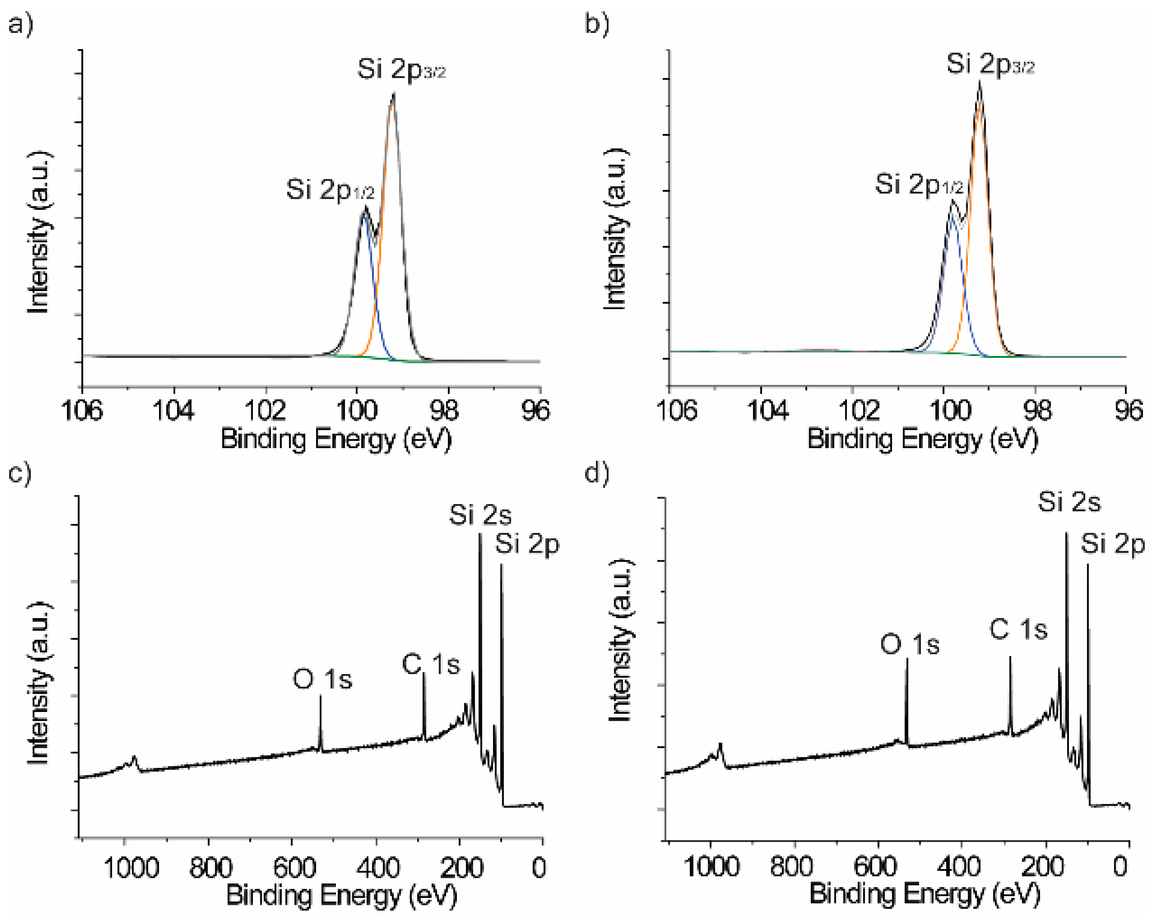
Figure 4.
Electrochemical characterisation of S–3 which was etched by NH4F and KF, respectively. CV for S–3 which was etched by (a) NH4F and (b) KF at the scan rate of 0.1 V/s. (c) The associated surface coverages were calculated from integration of the oxidation signals of the CV in (a,b). The error bars in (c) are shown as the standard deviation for the surface coverages obtained from the mean values of at least three different surfaces.

Figure 5.
Nyquist plots from EIS measurements for S–3 which was etched by (a) NH4F. (b) KF. (c) Bode plots for S–3 which was etched in different solution in frequency range from 10 Hz to 60,000 Hz. Scattered dots (black and blue) are experimental data, and lines (red and magenta) are the best fit to the experimental data. (d) The evolution of ket obtained by fitting the impedance data to the Randles circuit (Figure S2, Supplementary Materials). The error bars in (d) are the standard deviations of the ket values obtained from the mean values of three different surfaces.

Disclaimer/Publisher’s Note: The statements, opinions and data contained in all publications are solely those of the individual author(s) and contributor(s) and not of MDPI and/or the editor(s). MDPI and/or the editor(s) disclaim responsibility for any injury to people or property resulting from any ideas, methods, instructions or products referred to in the content. |
© 2024 by the authors. Licensee MDPI, Basel, Switzerland. This article is an open access article distributed under the terms and conditions of the Creative Commons Attribution (CC BY) license (https://creativecommons.org/licenses/by/4.0/).
Share and Cite
MDPI and ACS Style
Li, T.; Datson, Z.; Darwish, N. Formation of Organic Monolayers on KF-Etched Si Surfaces. Surfaces 2024, 7, 358-368. https://doi.org/10.3390/surfaces7020022
AMA Style
Li T, Datson Z, Darwish N. Formation of Organic Monolayers on KF-Etched Si Surfaces. Surfaces. 2024; 7(2):358-368. https://doi.org/10.3390/surfaces7020022
Chicago/Turabian StyleLi, Tiexin, Zane Datson, and Nadim Darwish. 2024. "Formation of Organic Monolayers on KF-Etched Si Surfaces" Surfaces 7, no. 2: 358-368. https://doi.org/10.3390/surfaces7020022