


AC Characteristics of van der Waals Bipolar Junction Transistors Using an MoS2/WSe2/MoS2 Heterostructure

State Key Laboratory of Optoelectronic Materials and Technologies, Guangdong Province Key Laboratory of Display Material and Technology, School of Electronics and Information Technology, Sun Yat-sen University, Guangzhou 510275, China
*
Author to whom correspondence should be addressed.
Nanomaterials 2024, 14(10), 851; https://doi.org/10.3390/nano14100851
Submission received: 24 March 2024
/
Revised: 4 May 2024
/
Accepted: 11 May 2024
/
Published: 14 May 2024
(This article belongs to the Special Issue 2D Layered Nanomaterials and Heterostructures for Electronics, Optoelectronics and Sensing)
Abstract
:Two-dimensional layered materials, characterized by their atomically thin thicknesses and surfaces that are free of dangling bonds, hold great promise for fabricating ultrathin, lightweight, and flexible bipolar junction transistors (BJTs). In this paper, a van der Waals (vdW) BJT was fabricated by vertically stacking MoS2, WSe2, and MoS2 flakes in sequence. The AC characteristics of the vdW BJT were studied for the first time, in which a maximum common emitter voltage gain of around 3.5 was observed. By investigating the time domain characteristics of the device under various operating frequencies, the frequency response of the device was summarized, which experimentally proved that the MoS2/WSe2/MoS2 BJT has voltage amplification capability in the 0–200 Hz region. In addition, the phase response of the device was also investigated. A phase inversion was observed in the low-frequency range. As the operating frequency increases, the relative phase between the input and output signals gradually shifts until it is in phase at frequencies exceeding 2.3 kHz. This work demonstrates the signal amplification applications of the vdW BJTs for neuromorphic computing and wearable healthcare devices.
1. Introduction
Bipolar junction transistors (BJTs), as some of the important semiconductor devices, have attracted great attention in past decades. They contain three separately doped regions, which are defined as the collector, base, and emitter. Two-dimensional (2D) materials offer significant opportunities for the construction of high-performance BJTs owing to their unique interlayered van der Waals (vdW) bonding characteristics [1,2,3]. By employing mechanical exfoliation or chemical vapor deposition (CVD), monolayer or multilayer 2D materials, including hexagonal boron nitride (h-BN) [4,5], transition metal dichalcogenides (TMDs) [6,7,8,9], and graphene [10,11,12], can be easily obtained. These ultrathin 2D materials provide possibilities for fabricating vdW BJTs with base regions of atomic thicknesses.
In the past few years, several 2D-material-based BJTs, such as BP/MoS2/BP [13,14,15,16], Cu9S5/PtS2/WSe2 [17], and MoS2/WSe2/MoS2 [18,19,20], have been fabricated successively. The static characteristics of these devices have been extensively studied, and they show promising application potential in the fields of photodetection [21,22], gas sensing [23,24], and biosensing [25]. However, the AC characteristics of vdW BJTs fabricated from 2D materials have not been reported yet, which is crucial for determining a device’s ability to process alternating signals.
In this paper, we report on a vdW BJT that was constructed by vertically stacking MoS2, WSe2, and MoS2 flakes in sequence. The static and AC characteristics of the device were investigated in a common emitter configuration. A maximum voltage gain of around 3.5 was observed in the low-frequency range. As the operating frequency increased, the voltage gain gradually decreased to unity at 200 Hz, and the relative phase between input and output signals gradually changed from 180° to 0° at 2.3 kHz. This systematic investigation of vdW BJTs provides a direct understanding of the electrical behavior of such devices under alternating current conditions, which could potentially aid in the utilization of the vdW BJTs in wearable healthcare devices and future neuromorphic applications.
2. Materials and Methods
2.1. Device Fabrication
A controlled multistep dry transfer process was employed to fabricate the vdW BJT [26]. Firstly, the WSe2 and MoS2 flakes were exfoliated from the bulk crystals supplied by HQ Graphene Company (Groningen, The Netherlands). Then, using the dry transfer technique, MoS2, WSe2 and MoS2 sheets were stacked onto a clean 300 nm SiO2/Si substrate in sequence. In this case, the top and bottom MoS2 sheets were separated by the middle WSe2 flake. Thirdly, maskless lithography was utilized to define the locations of the metal electrodes and thermal evaporation was employed to deposit Cr/Ag metals with thicknesses of 10 nm and 100 nm. Finally, the device underwent a two-hour annealing process in an argon atmosphere at 300 °C to eliminate the photoresistant residues and potentially facilitate Ag diffusion into the underlying MoS2 flakes, thereby reducing the contact resistance [27].
2.2. Characterization
AFM (NTEGRA Spectra, NT-MDT, Moscow, Russia) and Raman spectroscopy (In Via Reflex, Renishaw, Wotton-under-Edge, Gloucestershire, UK) instruments were employed to characterize the height profile and composition of the vdW BJT. A semiconductor parameter analyzer (B1500A, Agilent Technologies, Santa Clara, CA, USA) was used to investigate the static characteristics of the device. The AC performance of the vdW BJT was measured using an oscilloscope (DPO 7354C, Tektronix, Portland, OR, USA) and an arbitrary waveform generator (DG4062, RIGOL, Beijing, China).
3. Results and Discussion
Figure 1a,b show the schematic diagram and the optical image of the vertically stacked MoS2/WSe2/MoS2 BJT. Here, the top MoS2 sheet acts as the collector (C) while the bottom MoS2 sheet serves as the emitter (E). The multilayer WSe2 sheet was designed for the base (B) region. Figure 1c shows the height profile of the device. Apparently, the thicknesses of bottom MoS2, middle WSe2, and top MoS2are 13 nm, 3.5 nm, and 63.9 nm, respectively. To analyze the composition of the device, Raman spectra were obtained for the individual 2D materials as well as their overlap regions, as shown in Figure 1d. From the bottom MoS2, Raman peaks at 383.7 and 408.8 cm−1 can be observed. The two Raman peaks have a relatively large separation of 25.1 cm−1, confirming the multilayer nature of the MoS2 material [28,29]. The peaks at 249.8 and 258.3 cm−1 for the WSe2 flake are ascribed to the mode and the A1g mode [30]. In addition, the Raman spectra of the three flake overlap region are the sum of the Raman peaks of the MoS2 and WSe2 flakes, thereby confirming the successful fabrication of the vertically stacked heterostructure [31].
The static performance of the vdW BJT in common base mode was initially investigated. In this case, the base was grounded, whereas the base–collector and base–emitter junctions were separately reverse-biased and forward-biased. The band diagram of the vdW BJT operating in the forward-active operating mode is depicted in Figure 2a. Figure 2b shows the relationship between the base–emitter voltage (VBE) and the emitter current (IE) at various fixed collector–base voltages (VCB). With the increase in VBE, the depletion region of the base–emitter junction narrows, facilitating an enhanced diffusion of electrons from emitter to base. Hence, IE increased with a larger VBE. Figure 2c illustrates the output characteristic of the vdW BJT. The VBE can effectively affect the collector current (IC), since it can influence the electrons diffusing from the emitter. The electrons were transferred into the collector, constituting the main component of the IC. The common base current gain (α) was determined to be around 1.01 at VBE = 5 V by calculating the ratio of IC and IE. Figure 2d shows the output performance of the vdW BJT operating in common emitter mode. At low VCE values, the collector current shows an approximately linear increase with the VCE, indicating the saturation region of the device [13]. Beyond the saturation region, changes in VCE have minimal impact on the IC. Instead, the IC is primarily influenced by variations in VBE. This region is defined as the active region of the device. A maximum current gain (β = IC/IB) of approximately 9 can be obtained at VBE = 0.4 V under the common emitter configuration, as shown in Figure 2d. It is noteworthy that the MoS2/WSe2/MoS2 BJT has a relatively low on/off ratio, which may be attributed to the ultrathin base region. The negatively biased base–collector junction introduces an extra electric field perpendicular to the base–emitter junction, thereby diminishing the device’s on/off ratio [19,23].
Since the device showed excellent static performance, the AC characteristics of the vdW BJT operating in common emitter mode were investigated. The schematic diagram of the electrical connection is shown in Figure 3a. Here, a DC voltage (VBE = 5.8 V) and a small AC voltage (vi) were applied to the base–emitter junction. The base–collector junction was reverse-biased by connecting the collector to another power supply (VCE = 34 V) through a load resistor (RL = 22 MΩ). An oscilloscope was used to monitor the input and output waveforms of the device in real time. Figure 3b illustrates the time domain characteristics of the device operating at 1 Hz. Here, an AC voltage vi with an amplitude of 0.2 V is superimposed on the VBE, which causes the voltage applied on the base–emitter junction to fluctuate sinusoidally above and below its DC bias level. The resulting variation in IB causes the output current change. Therefore, an output AC signal with an amplitude approximately 3.5 times higher than the input AC signal can be observed in the collector region.
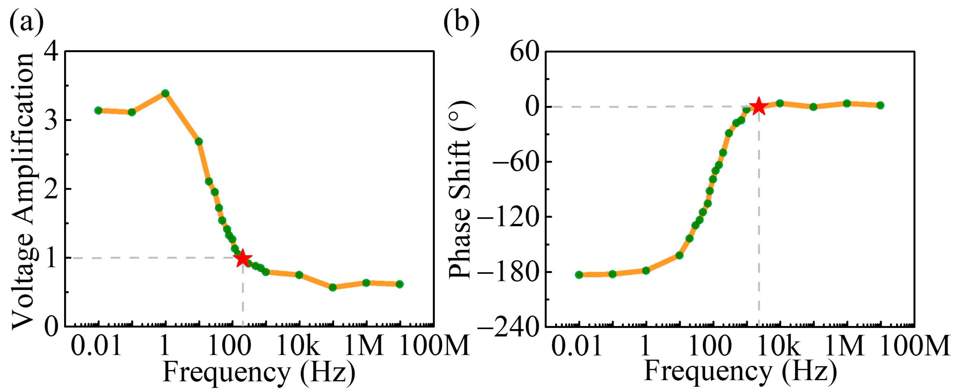
The time domain characteristics of the vdW BJT operating at other frequencies were also investigated. The representative results, such as for the device operating at 50 Hz and 1 kHz, are shown in Figure 3c,d. It is worth mentioning that the voltage in the collector region was higher than that in the base region throughout the experiment, which indicates that the BJT remained in forward-active operating mode at all times. Figure 4a summarizes the common emitter voltage gain versus the operating frequency. With the increase in operating frequency, the amplitude of the output voltage signal gradually decreases until the voltage gain falls to unity at 200 Hz, indicating that the device has voltage amplification capability in the 0–200 Hz region. Figure 4b illustrates the phase response of the device. The output signal at the collector region is 180° out of phase with the input signal in the low-frequency range. As the operating frequency increases, the relative phase between the input and output signals begins to shift until the output signal is in phase with the input signal at 2.3 kHz.
Further, the frequency response of the β value can be evaluated according to the time domain characteristics of the device operating at different frequencies, as illustrated in Figure 3b–d. Here, the output current (iC) of the device can be determined from the output signal (uo) by applying the formula iC = (VCE − uo)/RL. As the operating frequency continuously increases, the amplitude of iC is unchanged at first and then gradually decreases when the operating frequency exceeds 1 Hz. However, the input current (iB) is almost unaffected by the operating frequency. Therefore, the β value changing with the frequency is consistent with the trend of iC changing with the frequency; that is, it decreases as the operating frequency increases. In addition, to investigate the repeatability of the AC performance of the device, several other vdW BJTs with similar configurations were fabricated and investigated. All devices exhibited similar AC characteristics. The typical test results are shown in Figure S1 of the Supplementary Materials. The performance of the 2D-material-based n-p-n BJTs reported in the literature is summarized in Table 1 [14,18,19,20,23,25].
4. Conclusions
In summary, a vdW BJT was fabricated by vertically stacking MoS2, WSe2, and MoS2 flakes in sequence. The static characteristics of the device were investigated in common emitter and common base modes, demonstrating excellent current modulation and saturation characteristics. The AC performance of the device in common emitter mode was also investigated. A phase inversion from output to input with a maximum voltage gain of around 3.5 was obtained in the low-frequency range. As the operating frequency increases, the voltage gain gradually decreases to unity at 200 Hz and the relative phase between the input and output signals gradually changes to 0° at 2.3 kHz. This work demonstrates the AC characteristics of the vdW BJT and experimentally proves the device’s ability to process alternating signals. If the issues of device array fabrication and device-to-device variation can be further addressed, this will significantly promote the application of vdW BJTs as neuromorphic devices and wearable healthcare devices.
Supplementary Materials
The following supporting information can be downloaded at https://www.mdpi.com/article/10.3390/nano14100851/s1: Figure S1. (a) Optical microscope image of the MoS2/WSe2/MoS2 BJT. (b–d) Time domain characteristics of the device operating at 1 Hz, 100 Hz, and 1 kHz, respectively. (e) The frequency response of the device. (f) The phase response of the device.
Author Contributions
S.D. and N.X. proposed and supervised the project. Z.Y. carried out the experiments and analyzed the data. Z.Y., N.X. and S.D. discussed and interpreted the results. Z.Y. and S.D. wrote the manuscript. All authors have read and agreed to the published version of the manuscript.
Funding
This research was funded by the National Key Basic Research Program of China (grant numbers 2019YFA0210200 and 2019YFA0210203), the Science and Technology Department of Guangdong Province, and the Fundamental Research Funds for the Central Universities.
Data Availability Statement
The data presented in this article are available upon request from the corresponding author.
Conflicts of Interest
The authors declare no conflict of interest.
References
- Liu, Y.; Weiss, N.O.; Duan, X.D.; Cheng, H.C.; Huang, Y.; Duan, X.F. Van der Waals heterostructures and devices. Nat. Rev. Mater. 2016, 1, 16042. [Google Scholar] [CrossRef]
- Frisenda, R.; Molina-Mendoza, A.J.; Mueller, T.; Castellanos-Gomez, A.; Van, D. Atomically thin p–n junctions based on two-dimensional materials. Chem. Soc. Rev. 2018, 47, 3339–3358. [Google Scholar] [PubMed]
- Castellanos-Gomez, A.; Duan, X.F.; Fei, Z.; Gutierrez, H.R.; Huang, Y.; Huang, X.Y.; Quereda, J.; Qian, Q.; Sutter, E.; Sutter, P. Van der Waals heterostructures. Nat. Rev. Methods Primers 2022, 2, 58. [Google Scholar] [CrossRef]
- Park, J.H.; Park, J.C.; Yun, S.J.; Kim, H.; Luong, D.H.; Kim, S.M.; Choi, S.H.; Yang, W.; Kong, J.; Kim, K.K.; et al. Large-Area Monolayer Hexagonal Boron Nitride on Pt Foil. ACS Nano 2014, 8, 8520–8528. [Google Scholar] [CrossRef]
- Ismach, A.; Chou, H.; Ferrer, D.A.; Wu, Y.P.; McDonnell, S.; Floresca, H.C.; Covacevich, A.; Pope, C.; Piner, R.; Kim, M.J.; et al. Toward the Controlled Synthesis of Hexagonal Boron Nitride Films. ACS Nano 2012, 6, 6378–6385. [Google Scholar] [CrossRef] [PubMed]
- Li, H.; Yin, Z.Y.; He, Q.Y.; Li, H.; Huang, X.; Lu, G.; Fam, D.W.H.; Tok, A.I.Y.; Zhang, Q.; Zhang, H. Fabrication of Single- and Multilayer MoS2 Film-Based Field-Effect Transistors for Sensing NO at Room Temperature. Small 2012, 8, 63–67. [Google Scholar] [CrossRef]
- Rhyee, J.S.; Kwon, J.; Dak, P.; Kim, J.H.; Kim, S.M.; Park, J.; Hong, Y.K.; Song, W.G.; Omkaram, I.; Alam, M.A.; et al. High-Mobility Transistors Based on Large-Area and Highly Crystalline CVD-Grown MoSe2 Films on Insulating Substrates. Adv. Mater. 2016, 28, 2316–2321. [Google Scholar] [CrossRef]
- Campbell, P.M.; Tarasov, A.; Joiner, C.A.; Tsai, M.Y.; Pavlidis, G.; Graham, S.; Ready, W.J.; Vogel, E.M. Field-effect transistors based on wafer-scale, highly uniform few-layer p-type WSe2. Nanoscale 2016, 8, 2268–2276. [Google Scholar] [CrossRef]
- Zhou, J.D.; Lin, J.H.; Huang, X.W.; Zhou, Y.; Chen, Y.; Xia, J.; Wang, H.; Xie, Y.; Yu, H.M.; Lei, J.C.; et al. A library of atomically thin metal chalcogenides. Nature 2018, 556, 355–359. [Google Scholar] [CrossRef]
- Novoselov, K.S.; Geim, A.K.; Morozov, S.V.; Jiang, D.; Zhang, Y.; Dubonos, S.V.; Grigorieva, I.V.; Firsov, A.A. Electric field effect in atomically thin carbon films. Science 2004, 306, 666–669. [Google Scholar] [CrossRef]
- Guo, W.; Wu, B.; Wang, S.; Liu, Y.Q. Controlling Fundamental Fluctuations for Reproducible Growth of Large Single-Crystal Graphene. ACS Nano 2018, 12, 1778–1784. [Google Scholar] [CrossRef] [PubMed]
- Guo, W.; Jing, F.; Xiao, J.; Zhou, C.; Lin, Y.W.; Wang, S. Oxidative-Etching-Assisted Synthesis of Centimeter-Sized Single-Crystalline Graphene. Adv. Mater. 2016, 28, 3152–3158. [Google Scholar] [CrossRef] [PubMed]
- Aftab, S.; Eom, J. Van der Waals 2D layered-material bipolar transistor. 2D Mater. 2019, 6, 035005. [Google Scholar] [CrossRef]
- Su, B.W.; Zhang, X.L.; Yao, B.W.; Guo, H.W.; Li, D.K.; Chen, X.D.; Liu, Z.B.; Tian, J.G. Laser Writable Multifunctional van der Waals Heterostructures. Small 2020, 16, e2003593. [Google Scholar] [CrossRef] [PubMed]
- Lee, G.; Pearton, S.J.; Ren, F.; Kim, J. Two-Dimensionally Layered p-Black Phosphorus/n-MoS2/p-Black Phosphorus Heterojunctions. ACS Appl. Mater. Interfaces 2018, 10, 10347–10352. [Google Scholar] [CrossRef] [PubMed]
- Su, B.W.; Yao, B.W.; Zhang, X.L.; Huang, K.X.; Li, D.K.; Guo, H.W.; Li, X.K.; Chen, X.D.; Liu, Z.B.; Tian, J.G. A gate-tunable symmetric bipolar junction transistor fabricated via femtosecond laser processing. Nanoscale Adv. 2020, 2, 1733–1740. [Google Scholar] [CrossRef] [PubMed]
- Yang, S.J.; Pi, L.J.; Li, L.; Liu, K.L.; Pei, K.; Han, W.; Wang, F.K.; Zhuge, F.W.; Li, H.Q.; Cheng, G.; et al. 2D Cu9S5/PtS2/WSe2 Double Heterojunction Bipolar Transistor with High Current Gain. Adv. Mater. 2021, 33, 2106537. [Google Scholar] [CrossRef]
- Lee, G.; Pearton, S.J.; Ren, F.; Kim, J. 2D Material-Based Vertical Double Heterojunction Bipolar Transistors with High Current Amplification. Adv. Electron. Mater. 2019, 5, 1800745. [Google Scholar] [CrossRef]
- Liu, L.W.; Xu, N.S.; Zhang, Y.; Zhao, P.; Chen, H.J.; Deng, S.Z. Van der Waals Bipolar Junction Transistor Using Vertically Stacked Two-Dimensional Atomic Crystals. Adv. Funct. Mater. 2019, 29, 1807893. [Google Scholar] [CrossRef]
- Lin, C.Y.; Zhu, X.D.; Tsai, S.H.; Tsai, S.P.; Lei, S.D.; Shi, Y.M.; Li, L.J.; Huang, S.J.; Wu, W.F.; Yeh, W.K.; et al. Atomic-Monolayer Two-Dimensional Lateral Quasi-Heterojunction Bipolar Transistors with Resonant Tunneling Phenomenon. ACS Nano 2017, 11, 11015–11023. [Google Scholar] [CrossRef] [PubMed]
- Li, H.; Ye, L.; Xu, J.B. High-Performance Broadband Floating-Base Bipolar Phototransistor Based on WSe2/BP/MoS2 Heterostructure. ACS Photonics 2017, 4, 823–829. [Google Scholar] [CrossRef]
- Lv, L.; Zhuge, F.W.; Xie, F.J.; Xiong, X.J.; Zhang, Q.F.; Zhang, N.; Huang, Y.; Zhai, T.Y. Reconfigurable two-dimensional optoelectronic devices enabled by local ferroelectric polarization. Nat. Commun. 2019, 10, 3331. [Google Scholar] [CrossRef]
- Afzal, A.M.; Iqbal, M.Z.; Dastgeer, G.; Nazir, G.; Mumtaz, S.; Usman, M.; Eom, J. WS2/GeSe/WS2 Bipolar Transistor-Based Chemical Sensor with Fast Response and Recovery Times. ACS Appl. Mater. Interfaces 2020, 12, 39524–39532. [Google Scholar] [CrossRef] [PubMed]
- Liu, L.W.; Xu, N.S.; Ke, Y.L.; Chen, H.J.; Zhang, Y.; Deng, S.Z. Sensing by Surface Work Function Modulation: High Performance Gas Sensing using van der Waals Stacked Bipolar Junction Transistor. Sens. Actuators B-Chem. 2021, 345, 130340. [Google Scholar] [CrossRef]
- Dastgeer, G.; Shahzad, Z.M.; Chae, H.; Kim, Y.H.; Ko, B.M.; Eom, J. Bipolar Junction Transistor Exhibiting Excellent Output Characteristics with a Prompt Response against the Selective Protein. Adv. Funct. Mater. 2022, 32, 2204781. [Google Scholar] [CrossRef]
- Yan, Z.; Xu, N.; Deng, S. Realization of High Current Gain for Van der Waals MoS2/WSe2/MoS2 Bipolar Junction Transistor. Nanomaterials 2024, 14, 718. [Google Scholar] [CrossRef] [PubMed]
- Abraham, M.; Mohney, S.E. Annealed Ag contacts to MoS2 field-effect transistors. J. Appl. Phys. 2017, 122, 115306. [Google Scholar] [CrossRef]
- Jiang, Y.R.; Wang, R.Q.; Li, X.P.; Ma, Z.N.; Li, L.; Su, J.; Yan, Y.; Song, X.H.; Xia, C.X. Photovoltaic Field-Effect Photodiodes Based on Double van der Waals Heterojunctions. ACS Nano 2021, 15, 14295–14304. [Google Scholar] [CrossRef] [PubMed]
- Thakur, D.; Sato, Y.; Sabarigresan, M.; Ramadurai, R.; Balakrishnan, V. Enhanced optical emission at MoS2-WS2 heterostructure interface with n-N junction. Appl. Surf. Sci. 2022, 606, 154923. [Google Scholar] [CrossRef]
- Xiao, J.W.; Zhang, Y.; Chen, H.J.; Xu, N.S.; Deng, S.Z. Enhanced Performance of a Monolayer MoS2/WSe2 Heterojunction as a Photoelectrochemical Cathode. Nano-Micro Lett. 2018, 10, 60. [Google Scholar] [CrossRef]
- Zhu, J.Q.; Yue, X.F.; Chen, J.J.; Wang, J.; Wan, J.; Bao, W.Z.; Hu, L.G.; Liu, R.; Cong, C.X.; Qiu, Z.J. Ultrasensitive Phototransistor Based on Laser-Induced P-Type Doped WSe2/MoS2 Van der Waals Heterojunction. Appl. Sci. 2023, 13, 6024. [Google Scholar] [CrossRef]
Figure 1.
(a) Schematic illustration of the vdW BJT. (b) Optical microscope image of the vdW BJT. The inside of the dashed brown square represents the three flake overlapped region. (c) Height profile of the device. The dashed lines indicate the horizontal position of the steps. The inset illustrates the corresponding AFM image. (d) Raman spectra of the bottom MoS2, middle WSe2, top MoS2, and MoS2/WSe2/MoS2 three flake overlap regions.

Figure 2.
(a) Band diagram of the vdW BJT operating in forward-active operating mode. The orange, green, and blue areas indicate the emitter, base, and collector region of the device, respectively. (b) The relationship between IE and VBE at various fixed VCB values. (c) The relationship between IC and VCB at various values of VBE. Inset shows α as a function of VCB at a fixed VBE = 5 V. (d) The relationship between IC and VCE at various fixed VBE values. Inset shows β as a function of VCE at a fixed VBE = 0.4 V.

Figure 3.
(a) Schematic diagram of the electric connection of the vdW BJT in common emitter mode. (b–d) Time domain characteristics of the vdW BJT operating at 1 Hz, 50 Hz, and 1 kHz, respectively. The yellow area demonstrates the relative phase between the input and output signals during one cycle of the sinusoidal signal.

Figure 4.
(a) The frequency response of the device. The red star represents the frequency corresponding to a voltage amplification of 1. (b) The phase response of the device. The red star represents the frequency when the input and output signals are in phase. The green dots represent experimental test results and are connected by orange lines.

Table 1.
Comparison of device performance results between this work and various previously reported 2D-material-based n-p-n BJTs [14,18,19,20,23,25].
| Materials | Structure | On Current (μA) | α (DC) | β (DC) | Cutoff Frequency (Hz) | Voltage Gain | Ref. |
|---|---|---|---|---|---|---|---|
| MoS2/WSe2/MoS2 | Vertical | 0.67 | 1.01 | 9 | ~200 | 3.5 | This work |
| MoS2/WSe2/MoS2 | Vertical | 0.001 | 0.97 | 12 | / | / | [19] |
| MoS2/WSe2/MoS2 | Vertical | 0.054 | ~1 | 150 | / | / | [18] |
| MoTe2/GeSe/MoTe2 | Vertical | 0.014 | 0.95 | 29.3 | / | / | [25] |
| WS2/GeSe/WS2 | Vertical | 7.48 | 1.11 | 20.7 | / | / | [23] |
| MoS2/WSe2/MoS2 | In-plane | 0.001 | / | 3 | / | / | [20] |
| MoS2/BP/MoS2 | Lateral | 0.06 | 0.98 | 41 | / | / | [14] |
Disclaimer/Publisher’s Note: The statements, opinions and data contained in all publications are solely those of the individual author(s) and contributor(s) and not of MDPI and/or the editor(s). MDPI and/or the editor(s) disclaim responsibility for any injury to people or property resulting from any ideas, methods, instructions or products referred to in the content. |
© 2024 by the authors. Licensee MDPI, Basel, Switzerland. This article is an open access article distributed under the terms and conditions of the Creative Commons Attribution (CC BY) license (https://creativecommons.org/licenses/by/4.0/).
Share and Cite
MDPI and ACS Style
Yan, Z.; Xu, N.; Deng, S. AC Characteristics of van der Waals Bipolar Junction Transistors Using an MoS2/WSe2/MoS2 Heterostructure. Nanomaterials 2024, 14, 851. https://doi.org/10.3390/nano14100851
AMA Style
Yan Z, Xu N, Deng S. AC Characteristics of van der Waals Bipolar Junction Transistors Using an MoS2/WSe2/MoS2 Heterostructure. Nanomaterials. 2024; 14(10):851. https://doi.org/10.3390/nano14100851
Chicago/Turabian StyleYan, Zezhang, Ningsheng Xu, and Shaozhi Deng. 2024. "AC Characteristics of van der Waals Bipolar Junction Transistors Using an MoS2/WSe2/MoS2 Heterostructure" Nanomaterials 14, no. 10: 851. https://doi.org/10.3390/nano14100851
Note that from the first issue of 2016, this journal uses article numbers instead of page numbers. See further details here.