
Analysis of Scalable Resonant DC–DC Converter Using GaN Switches for xEV Charging Stations


1
Department of Electrical and Electronics Engineering, Vignan’s Foundation for Science Technology and Research, Guntur 522213, India
2
Mobility Group, Eaton India Innovation Center LLP, Pune 411028, India
3
Wenzhou Jiangcheng Automotive Parts Co., Ltd., Wenzhou 325400, China
*
Author to whom correspondence should be addressed.
World Electr. Veh. J. 2024, 15(5), 218; https://doi.org/10.3390/wevj15050218
Submission received: 7 April 2024
/
Revised: 10 May 2024
/
Accepted: 12 May 2024
/
Published: 17 May 2024
Abstract
:In this research, an innovative electric vehicle (EV) charger is designed and presented for xEV charging stations. The key feature of our system is a scalable, interleaved inductor–inductor–capacitor (iL2C) DC-DC converter operation. The proposed system employs two parallel L2C converters with 8-GaN switches on the primary side and a shared rectifier circuit on the secondary side. This configuration not only amplifies the resonant tank internal currents and losses generated by the switches but also improves current sharing. A novel closed-loop technique is proposed with a constant-voltage method of operation, along with a hybrid control scheme of variable frequency + phase shift modulation (VFPSM). To examine the controller and converter’s performance, an experimental demonstration is conducted under varying load conditions, including full load, half load, and light load, where the source voltage and load voltage are maintained at constant levels of 400 Vin and 48 V0, respectively. Furthermore, line regulation is conducted and verified to accommodate a broad input voltage range of 300 Vin–500 Vin and 500 Vin–300 Vin while maintaining an output voltage of 48 V0 at 3.3 kW, 1.65 kW, and 0.33 kW with a peak efficiency of 98.2%.
1. Introduction
Due to the contamination caused by toxic gases, carbon emissions, and unpredictable weather patterns, conventional internal combustion engines are approaching their maximum capabilities. There is a global initiative to implement environmentally friendly transportation in order to mitigate the effects of climate change. Electric vehicles (EVs) are increasingly becoming popular due to their environmentally advantageous nature, aiming to replace internal combustion engines (ICEs) and reduce carbon dioxide emissions [1,2,3]. By transitioning to electric vehicles, such as battery electric vehicles (BEVs), fuel cell electric vehicles (FCEVs), hybrid electric vehicles (HEVs), ultra-capacitor electric vehicles (UCEVs), solar-charged electric vehicles (SCEVs), and plug-in hybrid electric vehicles (PHEVs), we can significantly reduce pollutants [4,5]. The goal of achieving a carbon-free society by 2030 in Europe and 2050 in India is ambitious but achievable with the swift adoption of EVs and the development of robust charging infrastructure. This transition not only contributes to environmental preservation but also promotes technological advancement and energy independence. The increasing demand for electric vehicles necessitates the development of a strong and efficient charging infrastructure. The information in [6,7] covers power electronics for several applications such as solar energy, fuel cells, renewable energy, and electric cars. It also discusses optimization approaches for various charging topologies. Figure 1 illustrates a standard block diagram of a charging infrastructure.
In the present scenario, the EV industry is looking for a scalable design that can operate over wide operating ranges and easily adjust to different power requirements [8]. The need for scalability is increased because battery charging technology has improved over a wide range from 48 V to 800 V and even larger in some cases. The scalable designs are helpful with their quick adaptability of operation to the desired voltage range [9]. Resonant converters are more popular for their merit of operation over wide operating ranges; hence, this paper deals with an advanced resonant converter named the iL2C converter, which is an extension of the L2C converter [10,11].
According to our understanding, L2C resonant converters are gaining popularity in comparison to numerous traditional DC-DC converters [12,13]. This is due to their inherent benefits, including primary-side zero voltage switching (ZVS) operation across all load circumstances and secondary-side zero current switching (ZCS) operation with synchronous rectification [14,15]. The ZVS function can be compromised if the switching frequency, denoted as fs, is too low. Consequently, designers must take this into account when dealing with applications that require a wide voltage gain [16,17]. Furthermore, the use of the L2C converter as an EV charger is subject to many limitations. For instance, augmenting the load capacity at a high power density results in amplified voltage and current fluctuations, which can potentially harm the product [18,19]. The volume of the resonant tank is limited, resulting in increased circulating current and reduced efficiency [20].
This work introduces an iL2C converter as an electric vehicle charger to address the research gap in L2C converters [21]. In order to increase the load capacity, this converter employs two L2C converters operating in parallel. Consequently, the power losses in the transformer are reduced during high-current applications. Over time, numerous control techniques have been suggested to enhance soft switching, ensure precise regulation, and minimize the circulating current [22,23]. All of these control methods can be employed in different working areas of the converter, such as when the switching frequency (fs) is less than the resonant frequency (fr), when fs is equal to fr, and when fs is more than fr. These methods have an impact on the regulation of the converter. This article presents a hybrid control technique called the variable frequency + phase shift modulation (VFPSM) scheme. The strategy operates at a specified current value in either the zero current switching (ZCS) or zero voltage switching (ZVS) operating area. Furthermore, the iL2C DC-DC converter utilizes wideband gap semiconductor-based E-mode (enhancement mode) GaN technology.
The research contributions of this paper are as follows:
- The modeling of a scalable iL2C resonant converter with operation is presented.
- A hybrid control strategy is suggested and derived to improve the regulations.
- Simulations are presented for various load and line regulating conditions to check the converter performances.
- The experimental setup is demonstrated using E-mode GaN technology at 3.3 kW as an EV charger with an efficiency of 98.2%.
2. Modeling and Operation of iL2C Converter Topology
Figure 2 illustrates the resonant DC-DC topology of the iL2C, while Figure 3 depicts identical waveforms. It consists of two resonant circuits, each with a switching topology that incorporates a primary and secondary rectifier circuit utilizing a single diode bridge. It functions by employing a phase angle of 180° between the gate signals of two switching circuits. Equation (1) denotes that the resonant frequency of the converter is 150 kHz [21]. Additionally, the functioning of two switching topologies is comparable throughout their entire operational cycle; thus, the equations are examined in relation to the resonant network 1 and converter 1 [21,22]. The graphical representation of the gain performances of the converter is shown in Figure 4.
Stage 1: All secondary-side diodes are deactivated prior to time zero, while switches S2 and S3 are in the active state. During the time interval t0–t1, the switches S2 and S3 are deactivated, while the body diodes S1 and S4 are activated using a negative resonant current of iLr1.
Stage 2: The voltage throughout transformer 1 T1 is equivalent to the input voltage Vin between time points t1 and t2, and the switches S1, S4 and diodes D1, D4 are all in the ON state. Concurrently, the additional current of iNS1 conducts via the filter capacitor C0, while the resonant inductor Lr1 begins to circulate through the resonant capacitor Cr1. The voltage of the magnetizing inductance Lm1 is specified by Equation (2), and the current increases incrementally. Furthermore, the voltage across VNS1 from time t1 to time t2 is equivalent to the output voltage V0, as calculated in Equation (3), and subsequently, the voltage at the resonant tank is described in Equation (4) [24].
Stage 3: The switches S2 and S3 are activated at intervals t2 through t3, resulting in a positive current flow at iLr1, while the secondary-side diode rectifier circuit remains in an OFF state.
Stage 4: During the time intervals t3 to t4, the secondary-side diodes D2 and D4 are in the ON position in relation to the switches S2 and S3, because of the negative current circulation in iNS1. Consequently, the secondary-side voltage of the transformer is −VC0, which is exceedingly low, and the current iLm1 progressively diminishes. Conduction between the resonant inductor Lr1 and the resonant capacitor Cr1 commences simultaneously with the secondary current of iNS1 charging the filter capacitor C0. Equation (5) represents the voltage VNS1 at this juncture, while Equation (6) depicts the state space equation [24,25,26].
Stage 5: From time t4 to time t5, the components D2 and D3 are both in the ON state, while the secondary-side transformer current iNS1 is reduced to zero. Equation (7) represents the secondary side of the transformer voltage; consequently, the magnetizing inductance drops gradually [27,28]. Additionally, resonance occurs between the resonant capacitor Cr1 and the resonant inductor Lr1.
The state space equations for stage 5 are defined in Equation (8) below:
Stage 6: From time t5 to time t6, the current iNS1 on the secondary side of the transformer is entirely negative, accompanied by the absence of any diodes. The magnetizing inductance iLm1 begins to resonate with the resonant capacitor Cr1 and inductor Lr1 at this time.
The critical parameters of the iL2C converter for every single component are mentioned in [21,22,23,24]; the nominal input voltage is 400 V, and the output voltage is 48 V at a power range of 3.3 kW and a filter capacitor value of 100 µF, respectively. The associated step-by-step engineering calculations then followed with the appropriate values.
Equations (9)–(11) were utilized to derive a transformer T1 turn ratio of 8.82, as well as the maximum and minimum values of voltage gain of the iL2C converter under the specified operating conditions.
where n is transformer turn ratio, Vin_max and Vin_min are maximum and minimum input voltages, V0_max and V0_min are maximum and minimum output voltages, followed by maximum and minimum voltage gain Mmax and Mmin [24].
The resonant tank design of the resonant inductance Lr1 was 22.11 µH; the capacitance Cr1 was 50.94 nF; the impedance Z01 and the magnetizing inductance Lm1 were 20.83 Ω and 23 µH respectively with an equivalent resistance Rac1 of 22.12 Ω and 55.81 Ω as the minimum and maximum values. The formulas are mentioned in Equations (12)–(16) [29,30].
3. Control Strategy
There are now multiple control approaches being studied for resonant converters mainly based on fixed-or variable-frequency techniques and phase shifting strategies. Nevertheless, in practical use, each of them possesses distinct constraints when it comes to converters operating within a wider range of input and output voltages. Typically, frequency modulation is effective but necessitates intricate magnetic construction, whereas the phase shifting approach is straightforward to build but challenging for a wide variety of input voltages [24]. This paper presents a hybrid control methodology, known as the VFPSM method, for an iL2C converter. The VFPSM method ensures consistent control strategy performance throughout all areas.
The switching frequency fs is determined by comparing the output voltage V0 to the reference input voltage Vref, relying on the provided error voltage. The voltage control oscillator (VCO) can be utilized to compare the input and output voltage values [22,23,24], while also driving the gate signals. Figure 5 displays the control circuit. The controller regulates the output voltage V0 and modulates the current, referred to as the CV mode of operation. The third-order transfer function, specified in Equation (17) with sub-equations in Equations (18)–(22), is valuable for constructing the outer feedback compensator [31,32,33].
The development of the switching frequency design was concluded based on the information provided in Figure 5. This design enables the generation of pulses that may be used to switch the switches ON and OFF [34,35]. The 180-degree phase shift technique is employed to control the input voltage within the wide range of 300 Vin–500 Vin, while the VFPSM methodology ensures precise regulation at both the line and load sides [36]. The operation of converters 1 and 2 involves a switching process that utilizes the phase shifting approach known as “before 180°” and “after 180°”, respectively, as seen in Figure 6 [37,38].
4. Simulation and Experimental Validation
MATLAB/Simulink was utilized to conduct the simulation analysis of the iL2C converter employing the VFPSM control technique. The essential design variables are enumerated in [24]. The evaluation of the converter is provided for various case studies. In the first instance, the nominal input and output voltage under full load, half load, and light load conditions were examined. The nominal input voltage of 400 Vin is depicted as a constant in Figure 7.
The outcomes of the simulated converter were assessed under controlled nominal load conditions of 68.75 A and 48 V0 at maximum load (3.3 kW). Figure 8 shows the resonant tank waveforms of converter 1 and converter 2, and the converter load voltage and current waveforms are presented in Figure 9. The voltage and current ripple measurements indicated a deviation of +0.5 V (+1.04%) at a rated output of 48 V0 and approximately +0.65 A (+0.94%) at a full load current of 68.75 A, respectively.
Figure 10 shows the resonant tank waveforms of converter 1 and converter 2; Figure 11 presents the simulated results for the half load condition, which is at 1.65 kW, 48 V, and 34.375 A, respectively. At an output of 48 V0, both ripple voltages and currents were determined to have a voltage variance of +0.3 V (+0.62%) and a current variance of approximately +0.175 A (+0.5%) at a half load current of 38.375 A.
Figure 12 shows the resonant tank waveforms of converter 1 and converter 2; Figure 13 presents the simulated results at a light load which is 10% of the rated load, i.e., 0.33 kW, 48 V, and 6.875 A, respectively. At an output of 48 V0, both ripple voltages and currents were determined to have a voltage variance of +0.15 V (+0.31%) and a current variance of approximately +0.017 A (+0.25%) at a half load current of 6.875 A.
4.1. Dynamic Performance Analysis of iL2C Converter for 300 Vin–500 Vin under Various Load Conditions
In this section, the dynamic performance of the iL2C converter with a variable input voltage of 300–500 Vin and an output voltage that stays constant at 48 V0 is evaluated. The voltage increased abruptly from 300 to 500 Vin at 0.05 s, as depicted in Figure 14. Figure 15 illustrates the load voltage of 48 V and current waveforms at 3.3 kW. The sudden variation in load voltage and current took place at 0.05 s; the enlarged figures are also provided, and the settling time was within 1.1 ms.
Figure 16 illustrates the load voltage of 48 V and current waveforms at 1.65 kW. The sudden variation in load voltage and current took place at 0.05 s; the enlarged figures are also provided, and the settling time was within 1.0 ms.
Figure 17 illustrates the load voltage of 48 V and current waveforms at 0.33 kW. The sudden variation in load voltage and current took place at 0.05 s; the enlarged figures are also provided, and the settling time was within 1.3 ms.
4.2. Dynamic Performance Analysis of iL2C Converter for 500 Vin–300 Vin under Various Load Conditions
In this section, the dynamic performance of the iL2C converter with a variable input voltage of 500–300 Vin and an output voltage that stays constant at 48 V0 is evaluated. The voltage increased abruptly from 500 to 300 Vin at 0.05 s, as depicted in Figure 18. Figure 19 illustrates the load voltage of 48 V and current waveforms at 3.3 kW. The sudden variation in load voltage and current took place at 0.05 s; the enlarged figures are also provided, and the settling time was within 1.2 ms.
Figure 20 illustrates the load voltage of 48 V and current waveforms at 1.65 kW. The sudden variation in load voltage and current took place at 0.05 s; the enlarged figures are also provided, and the settling time was within 1.2 ms.
Figure 21 illustrates the load voltage of 48 V and current waveforms at 0.33 kW. The sudden variation in load voltage and current took place at 0.05 s; the enlarged figures are also provided, and the settling time was within 1.4 ms.
4.3. Experimental Validation of iL2C Converter
The iL2C converter concept is constructed utilizing GaN technology and operates at a maximum rated load capacity of 3.3 kW. The purpose of this prototype is to demonstrate the performance line and load regulation of the converter. The range of input voltages is set between 300 Vin and 500 Vin, while the rated load voltage is maintained at 48 V0. The converter’s effectiveness is evaluated under different load conditions [39,40]. The major side of the converter includes 8-GaN switches, specifically 4 in converter 1 and 4 in converter 2.
The production specifications of the GaN switch GS66508T are listed in [24], where the critical parameters are a drain source voltage of 650 V, a drain current of 30 A, and a low drain resistance of 50 mΩ, respectively. The E-mode GaN transistor possesses advanced characteristics such as an upper cooled technology, resulting in reduced junction–case thermal resistance at high power density [41,42]. It also exhibits decreased drain resistance, reverse recovery current, and zero reverse recovery losses. Additionally, it showcases well-designed gate charge characteristics [43]. The TMS320F28335 serves as the primary controller for the iL2C converter, functioning as a digital signal processor [44,45]. The prototype was constructed according to specific modeling parameters, including a magnetizing inductance of 23 µH for Lm1 and Lm2, resonant inductors of 21 µH for Lr1 and Lr2, resonant capacitors of 56 nF for Cr1 and Cr2, and a filter capacitor of 100 µF for C0. The experimental setup is illustrated in Figure 22.
Figure 23 displays the empirical waveforms of the drain and gate voltages of a switch operating with zero voltage switching (ZVS). This clearly demonstrates the successful attainment of ZVS functioning using soft switching.
The load regulation of the converter was analyzed and is depicted in Figure 24 under different load situations of 3.3 kW, 1.65 kW, and 0.33 kW. The input voltage was kept constant at 400 Vin, while the output voltage was maintained at 48 V0. Based on the findings, it was observed that the output voltage remained steady during load operations involving step-up and step-down conversion; this indicates effective voltage control. The findings were examined with a time scale of 100 ms for each division and a load voltage scale of 20 volts per division, shown by a blue line. The load current scale was set at 50 amperes per division, represented by a pink line. The input source voltage scale was set at 300 volts per division, represented by a red line.
As seen in Figure 25, the iL2C converter was validated for 3.3 kW at 48 V0 and 68.75 A during variable input voltage conditions. The findings were examined with a time scale of 100 ms for each division and a load voltage scale of 20 volts per division, shown by an orange line. The load current scale was set at 50 amperes per division, represented by a pink line. The input source voltage scale was set at 300 volts per division, represented by a blue line. The dynamic responses at the line side were executed by introducing an abrupt alteration in input voltage at 0.05 s (500 ms), resulting in a little modification in load voltage. The corresponding current was then monitored and recorded, as depicted in Figure 25. The converter and controller demonstrated conformity with the theoretical and simulated studies.
The efficiency of the GaN-powered iL2C converter was evaluated at the recommended voltage settings of 400 Vin and 48 V0. The efficiency was measured at various load conditions, specifically 3.3 kW, 3.0 kW, 2.5 kW, 2.0 kW, 1.65 kW, 1.0 kW, 0.5 kW, and 0.33 kW, sequentially. The efficiency was 98.2% at a power output of 3.3 kW, 98.7% at a power output of 1.65 kW, and 99.1% at a power output of 0.33 kW. Figure 26 displays the efficiency curve in relation to power.
5. Performance Analysis and Discussion
This section examines the steady-state and dynamic performance assessment of the converter in relation to line regulation and load regulation. The comparative assessment of simulation and experimental analysis of the converter was carried out during various conditions presented in Section 4. Moreover, the converter’s merits are discussed under various parameters at the end of this section.
5.1. Steady-State Performance Analysis
This analysis was conducted at constant input and load voltages, while varying the load. The voltage deviation and ripple percentage were measured to be +0.5 V (+1.04%), +0.3 V (+0.62%), and +0.15 V (+0.31%) at power levels of 3.3 kW, 1.65 kW, and 0.33 kW, respectively. Figure 27 and Figure 28 show the steady-state analysis under simulating conditions of load voltage deviation (LVD), average voltage ripple (%AVR), load current deviation (LCD), and average current ripple (%ACR), respectively [24]. The present discrepancy and fluctuation percentages were measured to be +0.65 A (+0.94%), +0.175 A (+0.5%), and +0.017 A (+0.25%) at power levels of 3.3 kW, 1.65 kW, and 0.33 kW, correspondingly.
The voltage variation and ripple percentage were measured to be +0.9 V (+1.87%), +0.7 V (+1.45%), and +0.52 V (+1.09%) for power levels of 3.3 kW, 1.65 kW, and 0.33 kW, respectively. Figure 29 and Figure 30 show the steady-state analysis under experimental conditions of LVD, %AVR, LCD, and %ACR, respectively [24]. The present difference and fluctuation percentages were measured as +1.26 A (+1.83%), +0.525 A (+1.52%), and +0.095 A (+1.23%) at power levels of 3.3 kW, 1.65 kW, and 0.33 kW, respectively.
5.2. Transient Performance Analysis
Table 1 shows the transient analysis during simulation conditions of the load voltage deviations, %avg load ripples, transient dip, and %avg dip of the voltage during line regulation (i.e., 300 Vin–500 Vin and 500 Vin–300 Vin) tabulated by maintaining the load voltage at 48 V0 and the load current at 68.75 A, 38.375 A, and 6.875 A, respectively. When the load was 3.3 kW, for (300 Vin–500 Vin) and (500 Vin–300 Vin), the max LVD was found to be +0.40 V and +0.42 V, and the %ALVR was +0.830% and +0.875%, respectively. The transient voltage dip was found to be +5.2 V, −3.5 V, and its average percentage dip was +10.83%, −7.29%, respectively, with a settling time of 1.1 ms and 1.2 ms. In the case of 1.65 kW, the max LVD was found to be +0.38 V and +0.40 V, and the %ALVR was +0.791% and +0.833%, respectively. The transient voltage dip was found to be +4.8 V, −5.8 V, and its average percentage dip was +10.00%, −12.08%, respectively, with a settling time of 1.0 ms and 1.2 ms. Lastly, in the case of 0.33 kW, the max LVD was found to be +0.37 V and +0.38 V, and the %ALVR was +0.770% and +0.791%, respectively. The transient voltage dip was found to be +6.35 V, −8.70 V, and its average percentage dip was +13.23%, −18.12%, respectively, with a settling time of 1.33 ms and 1.4 ms.
Table 2 shows the transient analysis during simulation conditions of the load current deviations, %avg load ripples, transient dip, and %avg dip of the current during line regulation (i.e., 300 Vin–500 Vin and 500 Vin–300 Vin) tabulated by maintaining the load voltage at 48 V0 and the load current at 68.75 A, 38.375 A, and 6.875 A, respectively. When the load was 3.3 kW, for (300 Vin–500 Vin) and (500 Vin–300 Vin), the max LCD was found to be +0.59 A and +0.64 A, and the %ALCR was +0.85% and +0.93%, respectively. The transient current dip was found to be +7.25 A, −4.75 A, and its average percentage dip was +10.54%, −6.90%, respectively, with a settling time of 1.1 ms and 1.2 ms. In the case of 1.65 kW, the max LCD was found to be +0.57 A and +0.62 A, and the %ALCR was +1.66% and +1.81%, respectively. The transient current dip was found to be +3.82 A, −2.25 A, and its average percentage dip was +11.11%, −6.54%, respectively, with a settling time of 1.0 ms and 1.2 ms. Lastly, in the case of 0.33 kW, the max LCD was found to be +0.055 A and +0.069 A, and the %ALCR was +0.8% and +1.0%, respectively. The transient current dip was found to be +1.85 A, −1.87 A, and its average percentage dip was +26.91%, −27.20%, respectively, with a settling time of 1.33 ms and 1.40 ms.
In addition, line regulations were conducted experimentally under variable input with a full load condition at 3.3 kW. Table 3 presents the comparative analysis of simulation and experimental conditions [24]. The simulation and experimental results indicate that the steady-state voltage deviation was +0.4 V (+0.83%) and +0.76 V (+1.58%), while the steady-state current deviation was +0.59 A (+0.85%) and +1.38 A (+2.0%), correspondingly.
The measurements in Table 4 indicate that there was a transient voltage dip (TVD) of +5.2 V (+10.83%), +6.17 V (+12.85%) and a transient current dip (TCD) of +7.25 A (+10.54%), +8.29 A (+12.05%), which are the transient voltage ripple (TVR) percentage and transient current ripple (TCR) percentage, respectively. The computational and experimental results indicate that the transient dip had a duration of 1.1 ms and 18 ms, respectively.
5.3. Discussion
The presented technology has the merit of scalability in operation, where it can operate in a wide range; ease of adaptability to any type of charging environment; and a high efficiency of operation. The major constraint of this technology is basically the construction of a complex system, and the management of the control algorithms for two bridges with maintaining the proper deadtime is the major challenge. The complexity of managing the two resonant tanks with hybrid structures will leads to a high cost of the system. The assembly, manufacturing, and fabrication of the proposed system having the higher involvement of complex strategies to minimize the losses during the development phase; this happens due to the system’s complexity.
6. Conclusions
This study focused on analyzing the iL2C resonant DC-DC converter, which utilizes a hybrid control method known as the variable frequency + phase shift modulation (VFPSM) technique. This research also contributes to the advancement of EV charging technology, ensuring efficient and reliable charging for xEVs. The converter is designed to accommodate a wide range of input voltages and is specifically intended for use in EV charging systems. This paper provides an explanation of the modeling and operational principles of the converter, and it conducts simulations of the whole proposed design using MATLAB/Simulink. The performance of the iL2C converter is evaluated under several conditions, and initially the converter is tested at various load and line conditions. Furthermore, the performance of the converter is verified through experimental validation utilizing GaN switches, and the results indicate that the controller effectively regulates the system. In future expansion of this work, predicative control techniques are to be implemented and analyzed.
Author Contributions
Conceptualization, R.P.N. and A.D.; Methodology, R.P.N. and A.S.T.; Validation, R.P.N.; Formal analysis, R.P.N. and S.M.; Investigation, R.P.N. and A.D.; Resources, R.P.N.; Writing—original draft, R.P.N. and A.S.T.; Writing—review & editing, R.P.N., S.M. and A.D.; Visualization, R.P.N.; Supervision, S.M., A.D. and A.S.T. All authors have read and agreed to the published version of the manuscript.
Funding
This research received no external funding.
Data Availability Statement
The original contributions presented in the study are included in the article, further inquiries can be directed to the corresponding author.
Conflicts of Interest
Rajanand Patnaik Narasipuram and Amit Singh Tandon are employees of Eaton India Innovation Center LLP. Anton Dianov is employee of Wenzhou Jiangcheng Automotive Parts Co., Ltd. The paper reflects the views of the scientists, and not the company.
Abbreviations
The abbreviations used in this paper are summarized as follows:
| BEV | Battery Electric Vehicle |
| ACR | Average Current Ripple |
| AVR | Average Voltage Ripple |
| E-mode | Enhancement Mode |
| EV | Electric Vehicle |
| FCEV | Fuel Cell Electric Vehicle |
| GaN | Gallium Nitride |
| HEV | Hybrid Electric Vehicle |
| ICE | Internal Combustion Engine |
| iL2C | Interleaved Inductor–Inductor–Capacitor |
| L2C | Inductor–Inductor–Capacitor |
| LCD | Load Current Deviation |
| LVD | Load Voltage Deviation |
| PHEV | Plugin Hybrid Electric Vehicle |
| SCEV | Super Capacitor Electric Vehicle |
| TCD | Transient Current Dip |
| TCR | Transient Current Ripple |
| TVD | Transient Voltage Dip |
| TVR | Transient Voltage Ripple |
| UCEV | Ultra-Capacitor Electric Vehicle |
| VCO | Voltage Control Oscillator |
| VFPSM | Variable Frequency Phase Shift Modulation |
| ZCS | Zero Current Switching |
| ZVS | Zero Voltage Switching |
References
- Mopidevi, S.; Narasipuram, R.P.; Aemalla, S.R.; Rajan, H. Emobility: Impacts and analysis of future transportation electrification market in economic, renewable energy and infrastructure perspective. Int. J. Powertrains 2022, 11, 264–284. [Google Scholar] [CrossRef]
- Zhou, K.; Wu, Y.; Wu, X.; Sun, Y.; Teng, D.; Liu, Y. Research and Development Review of Power Converter Topologies and Control Technology for Electric Vehicle Fast-Charging Systems. Electronics 2023, 12, 1581. [Google Scholar] [CrossRef]
- Shahjalal, M.; Shams, T.; Tasnim, M.N.; Ahmed, R.; Ahsan, M.; Haider, J. A Critical Review on Charging Technologies of Electric Vehicles. Energies 2022, 15, 8239. [Google Scholar] [CrossRef]
- Ilahi, T.; Izhar, T.; Zahid, M.; Rasool, A.; Tsamaase, K.; Zahid, T.; Khan, E.M. Design Analysis of High-Power Level 4 Smart Charging Infrastructure Using Next-Generation Power Devices for EVs and Heavy Duty EVs. World Electr. Veh. J. 2024, 15, 66. [Google Scholar] [CrossRef]
- Narasipuram, R.P.; Mopidevi, S. A technological overview & design considerations for developing electric vehicle charging stations. J. Energy Storage 2021, 43, 103225. [Google Scholar] [CrossRef]
- Deng, J.; Li, S.; Hu, S.; Mi, C.C.; Ma, R. Design Methodology of LLC Resonant Converters for Electric Vehicle Battery Chargers. IEEE Trans. Veh. Technol. 2014, 63, 1581–1592. [Google Scholar] [CrossRef]
- Domajnko, J.; Prosen, N. A Wireless Power Transfer System Using a Double DD Quadrature Coil Structure. Electronics 2023, 12, 890. [Google Scholar] [CrossRef]
- Far, M.F.; Miljavec, D.; Manko, R.; Pippuri-Mäkeläinen, J.; Ranta, M.; Keränen, J.; Kinder, J.; Vukotić, M. Modular and Scalable Powertrain for Multipurpose Light Electric Vehicles. World Electr. Veh. J. 2023, 14, 309. [Google Scholar] [CrossRef]
- Cervero, D.; Fotopoulou, M.; Muñoz-Cruzado, J.; Rakopoulos, D.; Stergiopoulos, F.; Nikolopoulos, N.; Voutetakis, S.; Sanz, J.F. Solid State Transformers: A Critical Review of Projects with Relevant Prototypes and Demonstrators. Electronics 2023, 12, 931. [Google Scholar] [CrossRef]
- Beiranvand, R.; Rashidian, B.; Zolghadri, M.R.; Alavi, S.M.H. A Design Procedure for Optimizing the LLC Resonant Converter as a Wide Output Range Voltage Source. IEEE Trans. Power Electron. 2012, 27, 3749–3763. [Google Scholar] [CrossRef]
- Musavi, F.; Craciun, M.; Gautam, D.S.; Eberle, W.; Dunford, W.G. An LLC resonant DC–DC converter for wide output voltage range battery charging applications. IEEE Trans. Power Electron. 2013, 28, 5437–5445. [Google Scholar] [CrossRef]
- Kim, B.-C.; Park, K.-B.; Kim, C.-E.; Moon, G.-W. Load sharing characteristic of two-phase interleaved LLC resonant converter with parallel and series input structure. In Proceedings of the 2009 IEEE Energy Conversion Congress and Exposition (ECCE), San Jose, CA, USA, 20–24 September 2009; pp. 750–753. [Google Scholar]
- Guo, B.; Zhang, Y.; Zhang, J.; Gao, J. Hybrid Control Strategy of Phase-Shifted Full-Bridge LLC Converter Based on Digital Direct Phase-Shift Control. J. Power Electron. 2018, 18, 802–816. [Google Scholar]
- Zhou, B.; Zhao, C.; Luo, H.; Qiu, Y.; Chen, S.; Zang, T.; Zhou, Y.; Zhou, X.; Zhao, H. Hybrid Control Strategy for Single-Stage Interleaved Totem-Pole LLC AC-DC Converter With Input and Output Power Decoupling. IEEE Trans. Power Electron. 2024, 39, 5135–5154. [Google Scholar] [CrossRef]
- Yoo, K.-M.; Lee, J.-Y. A 10-kW Two-Stage Isolated/Bidirectional DC/DC Converter with Hybrid-Switching Technique. IEEE Trans. Ind. Electron. 2013, 60, 2205–2213. [Google Scholar] [CrossRef]
- Mortazavizadeh, S.A.; Palazzo, S.; Amendola, A.; De Santis, E.; Di Ruzza, D.; Panariello, G.; Sanseverino, A.; Velardi, F.; Busatto, G. High Frequency, High Efficiency, and High Power Density GaN-Based LLC Resonant Converter: State-of-the-Art and Perspectives. Appl. Sci. 2021, 11, 11350. [Google Scholar] [CrossRef]
- Shadnam Zarbil, M.; Khalifeh, M.; Vahedi, A. A real-time LabVIEW-based emulator for various types of electrical loads. Electr. Eng. 2022, 104, 4367–4378. [Google Scholar] [CrossRef]
- Maurya, R.; Arya, S.R.; Saini, R.K.; Gupta, J. On-board power quality charger for electric vehicles with minimized switching stresses. Electr. Eng. 2022, 104, 1667–1680. [Google Scholar] [CrossRef]
- Bayati, M.; Abedi, M.; Gharehpetian, G.B.; Farahmandrad, M. Two designs for DC–DC stage of electric vehicle charging stations. Electr. Eng. 2020, 102, 2389–2399. [Google Scholar] [CrossRef]
- Wang, H.; Dusmez, S.; Khaligh, A. Design and analysis of a full-bridge LLC-based PEV charger optimized for wide battery voltage range. IEEE Trans. Veh. Technol. 2014, 63, 1603–1613. [Google Scholar] [CrossRef]
- Narasipuram, R.P.; Mopidevi, S. A Novel Hybrid Control Strategy and Dynamic Performance Enhancement of a 3.3 kW GaN–HEMT-Based iL2C Resonant Full-Bridge DC–DC Power Converter Methodology for Electric Vehicle Charging Systems. Energies 2023, 16, 5811. [Google Scholar] [CrossRef]
- Narasipuram, R.P.; Mopidevi, S. Parametric Modelling of Interleaved Resonant DC–DC Converter with Common Secondary Rectifier Circuit for xEV Charging Applications. In Proceedings of the 2023 International Conference on Sustainable Emerging Innovations in Engineering and Technology (ICSEIET), Ghaziabad, India, 14–15 September 2023; pp. 842–846. [Google Scholar]
- Narasipuram, R.P.; Mopidevi, S. A Dual Primary Side FB DC-DC Converter with Variable Frequency Phase Shift Control Strategy for On/Off Board EV Charging Applications. In Proceedings of the 2023 9th IEEE India International Conference on Power Electronics (IICPE), Sonipat, India, 28–30 November 2023; pp. 1–5. [Google Scholar]
- Narasipuram, R.P.; Mopidevi, S. An industrial design of 400 V-48 V, 98.2% peak efficient charger using E-mode GaN technology with wide operating ranges for xEV applications. Int. J. Numer. Model. Electron. Netw. Devices Fields 2024, 37, e3194. [Google Scholar] [CrossRef]
- Xi, J.; Si, H.; Gao, J. Optimization of a Shift Control Strategy for Pure Electric Commercial Vehicles Based on Driving Intention. World Electr. Veh. J. 2024, 15, 44. [Google Scholar] [CrossRef]
- Althurthi, S.B.; Rajashekara, K.; Debnath, T. Comparison of EV Fast Charging Protocols and Impact of Sinusoidal Half-Wave Fast Charging Methods on Lithium-Ion Cells. World Electr. Veh. J. 2024, 15, 54. [Google Scholar] [CrossRef]
- Zulauf, G.; Park, S.; Liang, W.; Surakitbovorn, K.N.; Rivas-Davila, J. COSS Losses in 600 V GaN Power Semiconductors in Soft-Switched, High- and Very-High-Frequency Power Converters. IEEE Trans. Power Electron. 2018, 33, 10748–10763. [Google Scholar] [CrossRef]
- Van Do, T.; Trovao, J.P.F.; Li, K.; Boulon, L. Wide-Bandgap Power Semiconductors for Electric Vehicle Systems: Challenges and Trends. IEEE Veh. Technol. Mag. 2021, 16, 89–98. [Google Scholar] [CrossRef]
- Gu, W.-J.; Harada, K. A new method to regulate resonant converters. IEEE Trans. Power Electron. 1988, 3, 430–439. [Google Scholar] [CrossRef]
- Bosshard, T.R.; Kolar, J.W. Performance comparison of a GaN GIT and a Si IGBT for high-speed drive applications. In Proceedings of the 2014 International Power Electronics Conference (IPEC-Hiroshima 2014—ECCE ASIA), Hiroshima, Japan, 18–21 May 2014. [Google Scholar]
- Narasipuram, R.P.; Karkhanis, V.A.; Ellinger, M.; Saranath, K.M.; Alagarsamy, G.; Jadhav, R. Systems Engineering—A Key Approach to Transportation Electrification. Symposium on International Automotive Technology; SAE Technical Paper, 2024-26-0128; SAE International: Warrendale, PA, USA, 2024. [Google Scholar]
- Elrajoubi, A.M.; Ang, S.S.; George, K. Design and analysis of a new GaN-Based AC/DC converter for battery charging application. IEEE Trans. Ind. Appl. 2019, 55, 4044–4052. [Google Scholar] [CrossRef]
- Pushpakaran, B.N.; Subburaj, A.S.; Bayne, S.B. Commercial GaN-Based Power Electronic Systems: A Review. J. Electron. Mater. 2020, 49, 6247–6262. [Google Scholar] [CrossRef]
- Keshmiri, N.; Wang, D.; Agrawal, B.; Hou, R.; Emadi, A. Current Status and Future Trends of GaN HEMTs in Electrified Transportation. IEEE Access 2020, 8, 70553–70571. [Google Scholar] [CrossRef]
- Chellappan, S. Design Considerations of GaN Devices for Improving Power Converter Efficiency; Texas Instruments Inc.: Dallas, TX, USA, 2017. [Google Scholar]
- Yadlapalli, R.T.; Kotapati, A.; Kandipati, R.; Balusu, S.R.; Koritala, C.S. Advancements in energy efficient GaN power devices and power modules for electric vehicle applications: A review. Int. J. Energy Res. 2021, 45, 12638–12664. [Google Scholar] [CrossRef]
- Lidow, A.; Strydom, J.; Strittmatter, R.; Zhou, C. GaN: A Reliable Future in Power Conversion: Dramatic performance improvements at a lower cost. IEEE Power Electron. Mag. 2015, 2, 20–26. [Google Scholar] [CrossRef]
- Will, C.; Ocker, F. Flexibility Potential of Smart Charging Electric Trucks and Buses. World Electr. Veh. J. 2024, 15, 56. [Google Scholar] [CrossRef]
- Lei, H.; Hu, X.; Zhao, J.; Deng, D.; Wang, R. Research Progress and Prospects of Public Transportation Charging Station Layout Methods. World Electr. Veh. J. 2024, 15, 63. [Google Scholar] [CrossRef]
- Zheng, J.; Du, Y.; Chen, D.; Ying, W.; Zhao, H.; Liu, K.; Qiu, J. Resonant Gate Drive Circuit with Active Clamping to Increase Efficiency and Reliability. World Electr. Veh. J. 2024, 15, 74. [Google Scholar] [CrossRef]
- Bernard, K. Advantages of Using Gallium NitrideFETs in Satellite Applications; Renesas: Tokyo, Japan, 2018. [Google Scholar]
- Wang, Y.; Ding, Y.; Yin, Y. Reliability of Wide Band Gap Power Electronic Semiconductor and Packaging: A Review. Energies 2022, 15, 6670. [Google Scholar] [CrossRef]
- Al Attar, H.; Hamida, M.A.; Ghanes, M.; Taleb, M. LLC DC-DC Converter Performances Improvement for Bidirectional Electric Vehicle Charger Application. World Electr. Veh. J. 2022, 13, 2. [Google Scholar] [CrossRef]
- Bottaro, E.; Rizzo, S.A.; Salerno, N. Circuit Models of Power MOSFETs Leading the Way of GaN HEMT Modelling—A Review. Energies 2022, 15, 3415. [Google Scholar] [CrossRef]
- Wei, Y.; Luo, Q.; Wang, Z.; Mantooth, H.A. A Complete Step-by-Step Optimal Design for LLC Resonant Converter. IEEE Trans. Power Electron. 2021, 36, 3674–3691. [Google Scholar] [CrossRef]
Figure 1.
Typical block diagram of charging power conversion system.

Figure 2.
iL2C DC-DC power converter topology [21].
Figure 2.
iL2C DC-DC power converter topology [21].

Figure 3.
Identical waveforms of interleaved L2C DC-DC switching network 1 [21].
Figure 3.
Identical waveforms of interleaved L2C DC-DC switching network 1 [21].

Figure 4.
Voltage gain M vs. frequency f by varying the Q-factor [21].
Figure 4.
Voltage gain M vs. frequency f by varying the Q-factor [21].

Figure 5.
Closed-loop controller using VCO for CV mode of operation [24].
Figure 5.
Closed-loop controller using VCO for CV mode of operation [24].

Figure 6.
VFPSM control strategy control block diagram [24].
Figure 6.
VFPSM control strategy control block diagram [24].

Figure 7.
Rated input voltage waveform (Vin = 400 V).
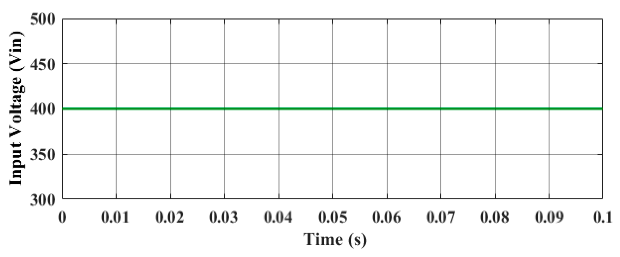
Figure 8.
Resonant tank waveforms of converter 1 and converter 2 at 3.3 kW.
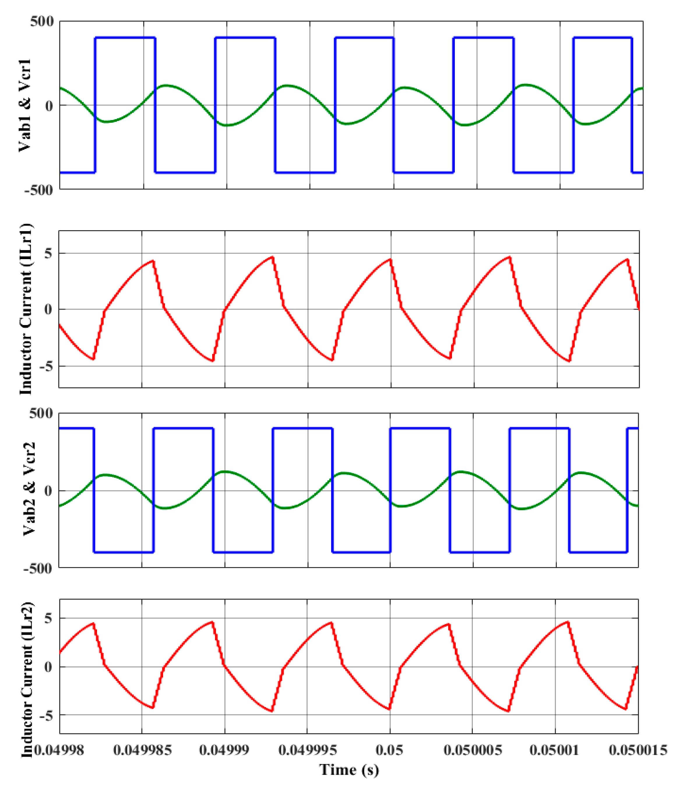
Figure 9.
Load voltage and current waveforms at full load (3.3 kW).

Figure 10.
Resonant tank waveforms of converter 1 and converter 2 at 1.65 kW.

Figure 11.
Load voltage and current waveforms at half load (1.65 kW).

Figure 12.
Resonant tank waveforms of converter 1 and converter 2 at 0.33 kW.
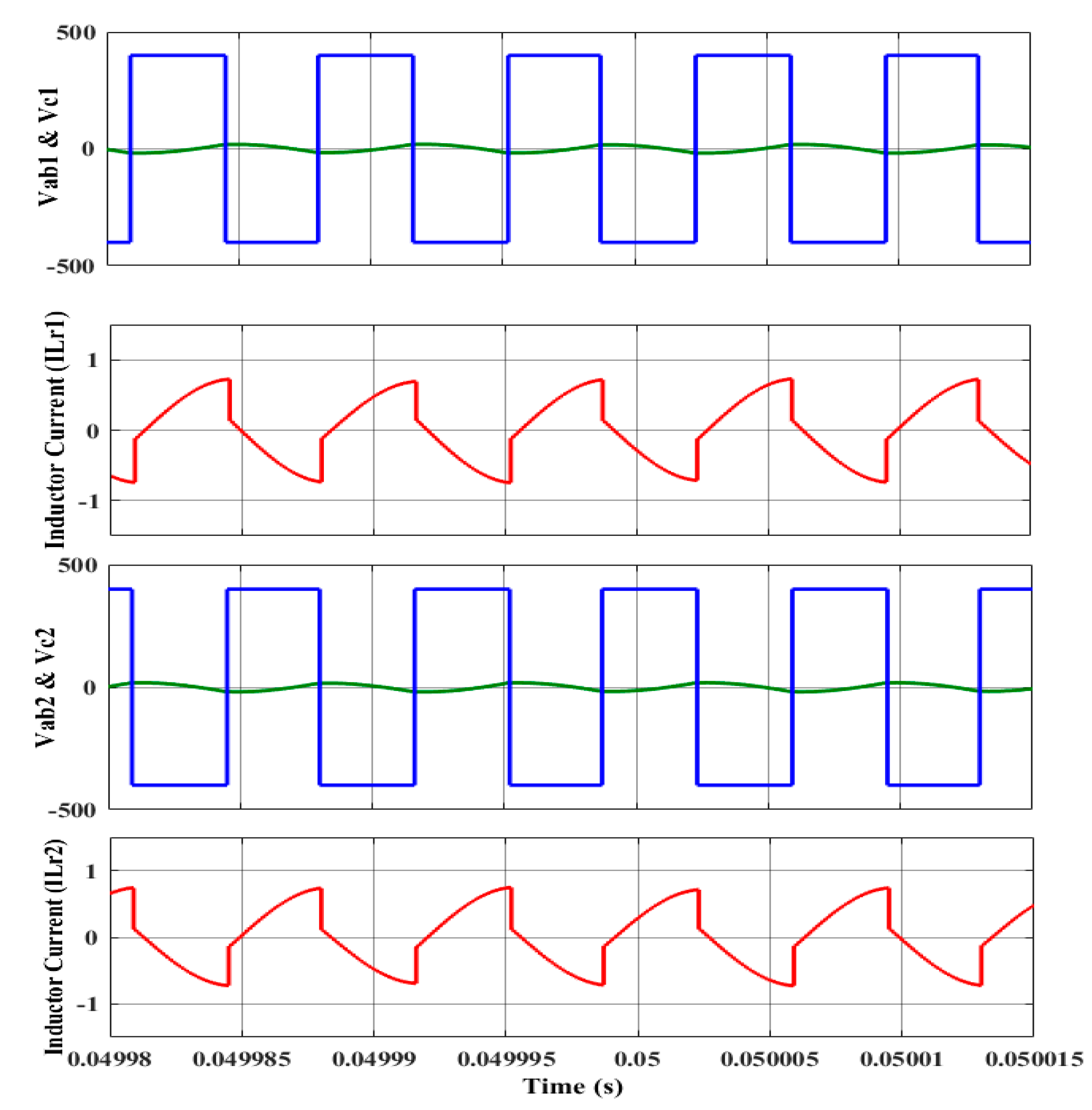
Figure 13.
Load voltage and current waveforms at light load (0.33 kW).

Figure 14.
Sudden change in input voltage from 300 Vin to 500 Vin at 0.05 s.

Figure 15.
Step change in load voltage and current waveforms from 300 Vin to 500 Vin at 3.3 kW.
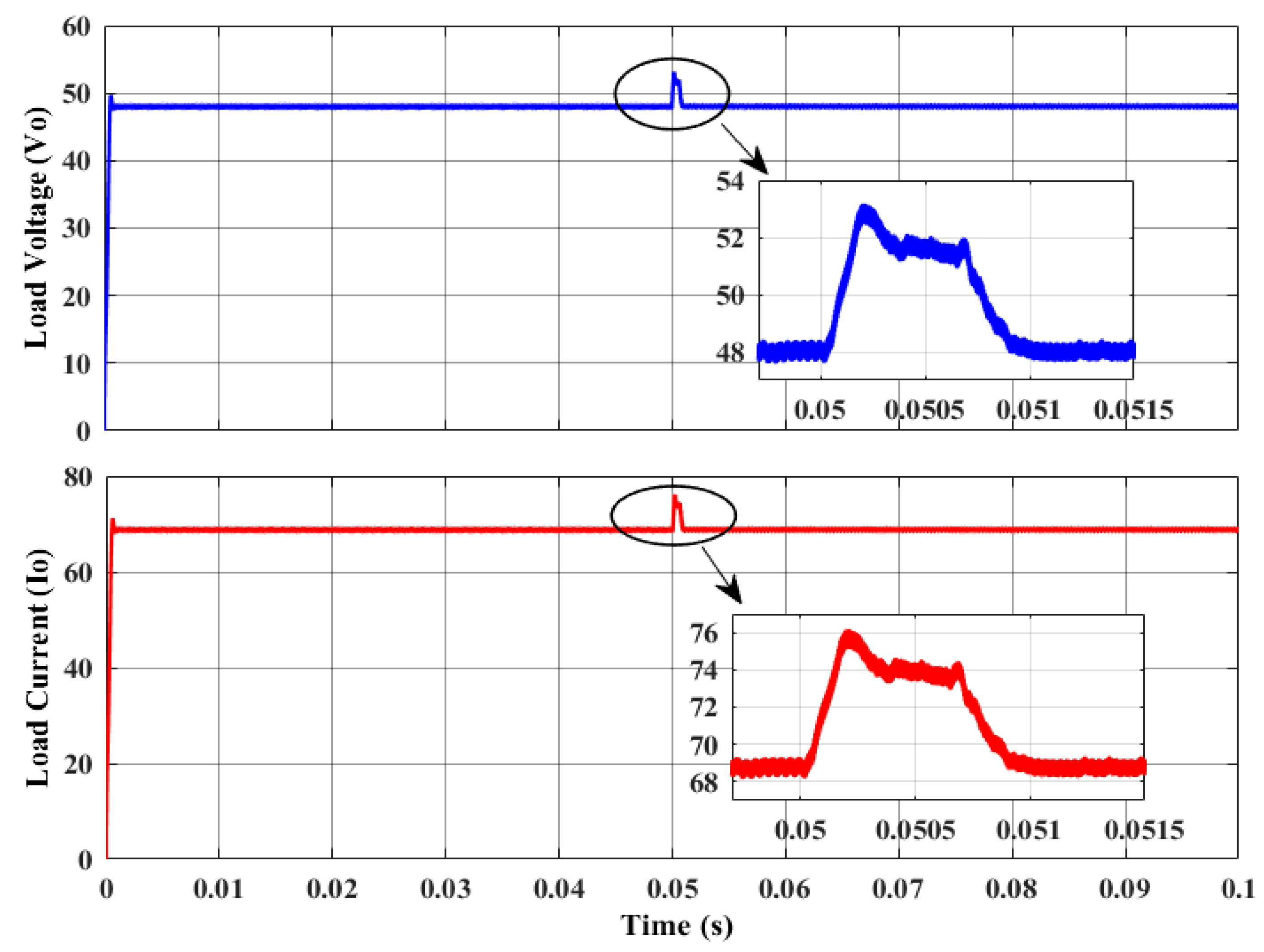
Figure 16.
Step change in load voltage and current waveforms from 300 Vin to 500 Vin at 1.65 kW.

Figure 17.
Step change in load voltage and current waveforms from 300 Vin to 500 Vin at 0.33 kW.

Figure 18.
Sudden change in input voltage from 500 Vin to 300 Vin at 0.05 s.

Figure 19.
Step change in load voltage and current waveforms from 500 Vin to 300 Vin at 3.3 kW.

Figure 20.
Step change in load voltage and current waveforms from 500 Vin to 300 Vin at 1.65 kW.
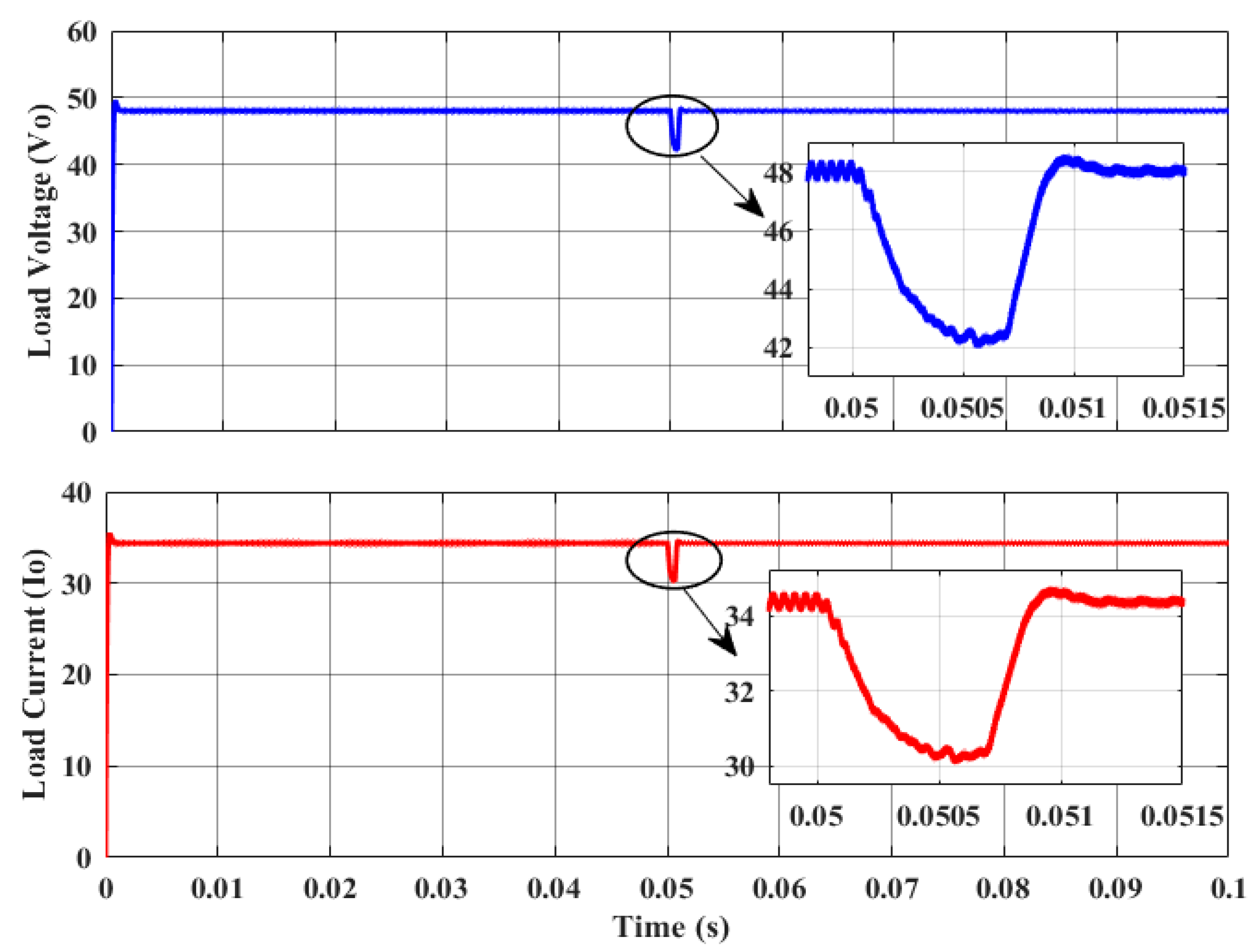
Figure 21.
Step change in load voltage and current waveforms from 500 Vin to 300 Vin at 0.33 kW.

Figure 22.
Experimental setup of iL2C converter for 3.3 kW [24].
Figure 22.
Experimental setup of iL2C converter for 3.3 kW [24].

Figure 23.
Validated waveforms of GaN switch VDS and VGS.

Figure 24.
Validated waveforms during load regulation.
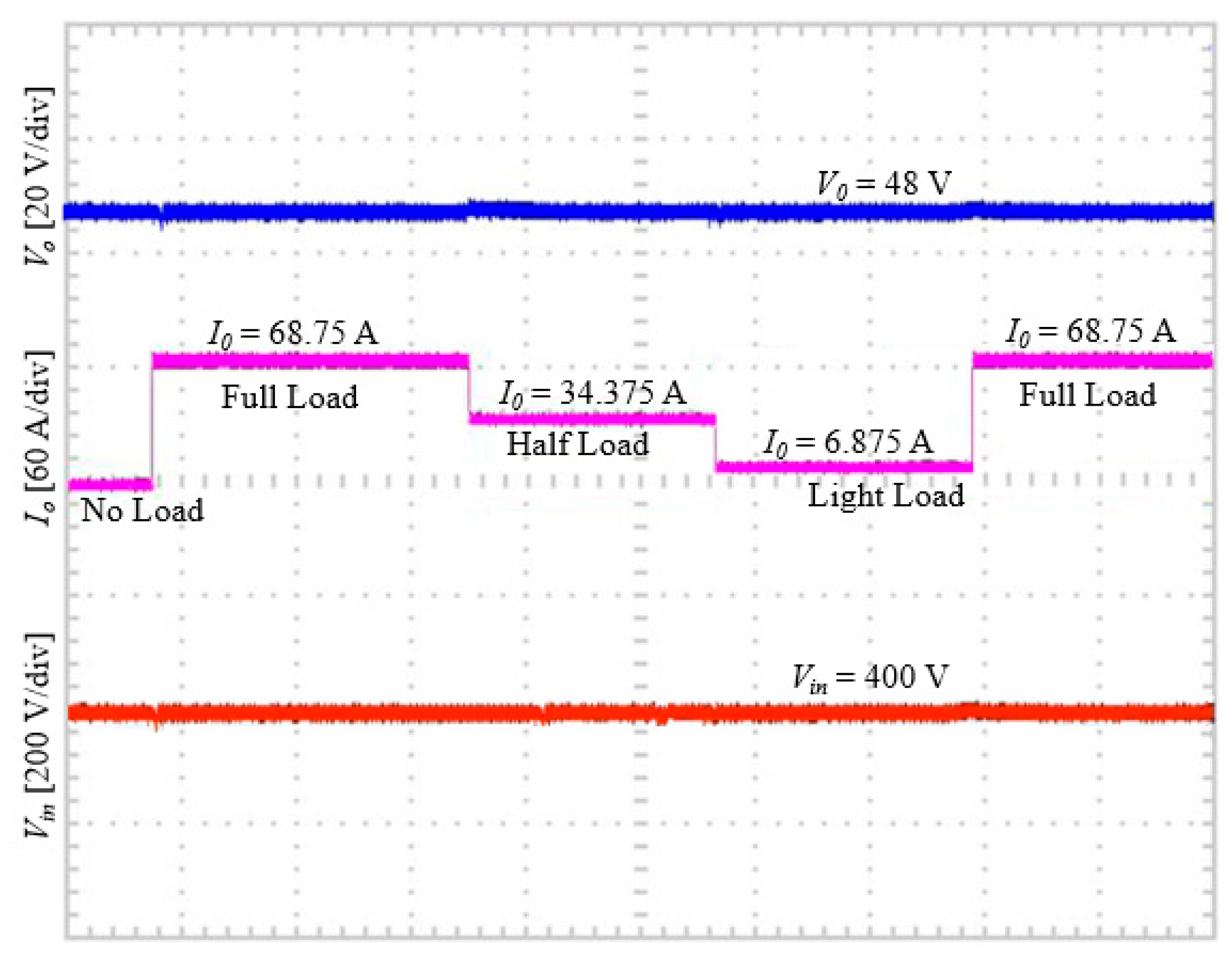
Figure 25.
Validated waveforms during regulated line voltage.

Figure 26.
Efficiency vs. power.
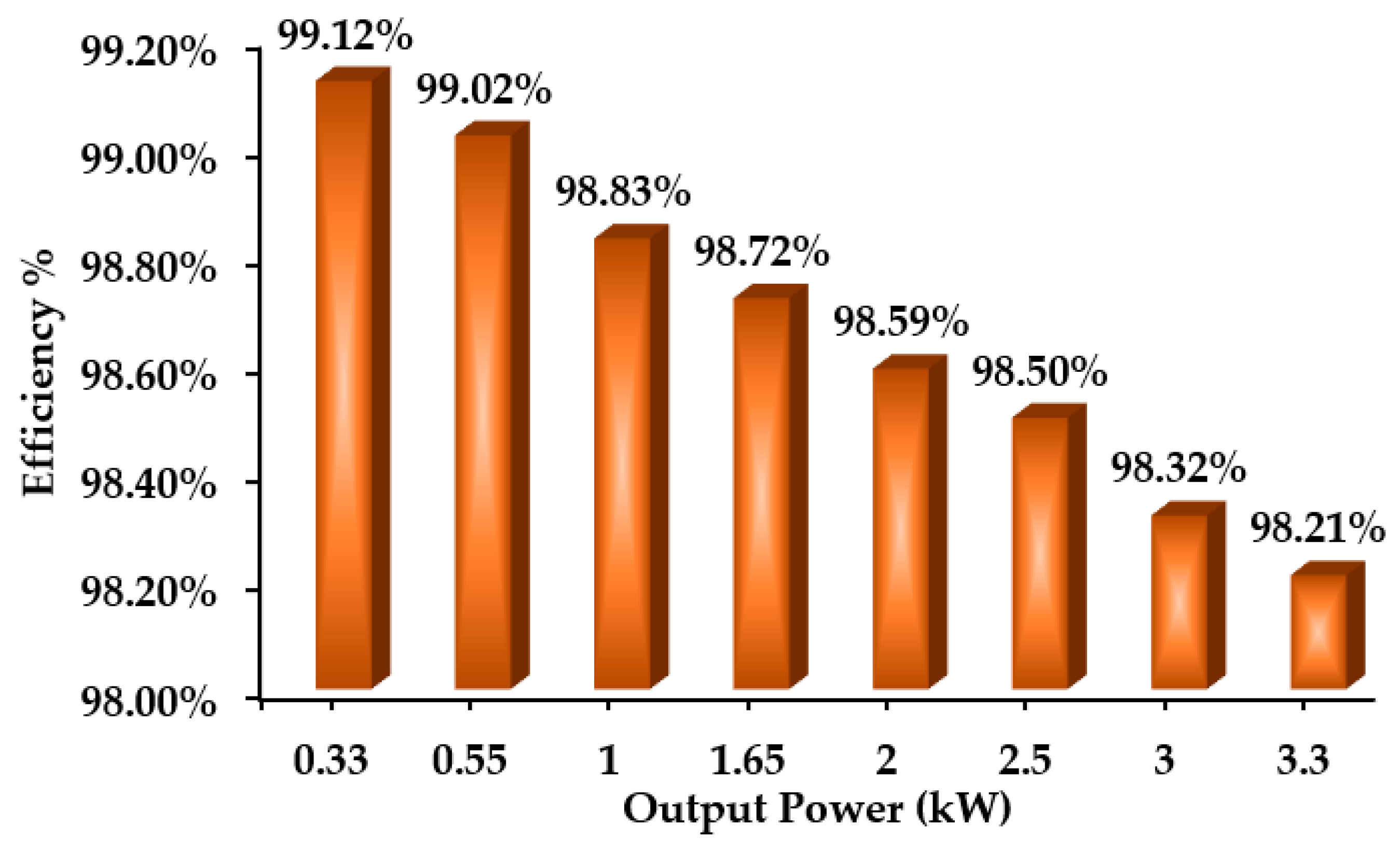
Figure 27.
Steady-state analysis of LVD vs. %AVR during simulations.
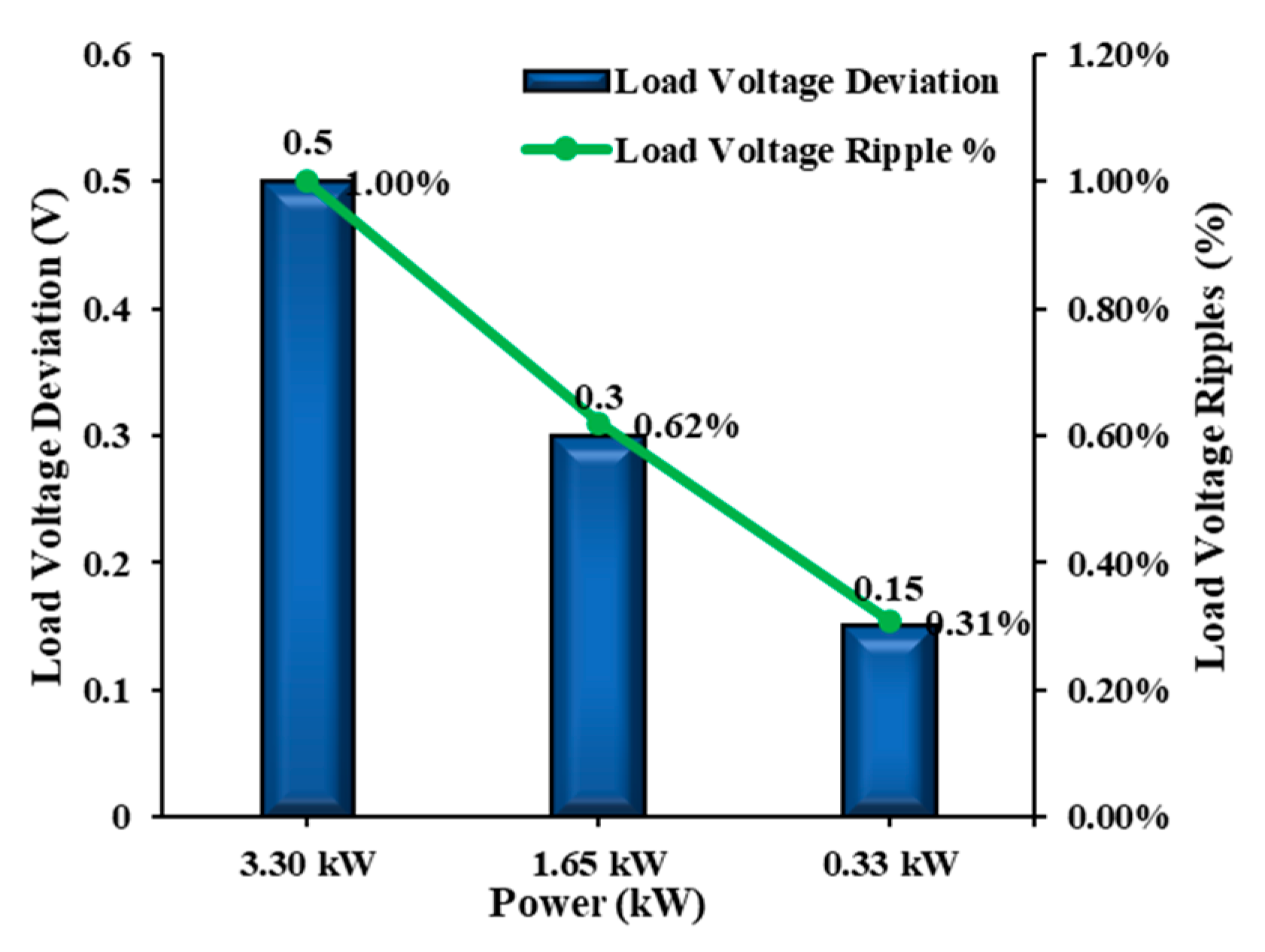
Figure 28.
Steady-state analysis of LCD vs. %ACR during simulations.

Figure 29.
Steady-state analysis of LVD vs. %AVR during experimental validation.

Figure 30.
Steady-state analysis of LCD vs. %ACR during experimental validation.


Table 1.
Transient analysis under line regulation during simulations.
| Operation Attributes | Variable Input Voltage | Max. LVD | % ALVR | Transient Analysis | |||
|---|---|---|---|---|---|---|---|
| Voltage Dip | Avg % of Dip | Settling Time | |||||
| Load Variation | 3.3 kW | 300 V–500 V | +0.40 V | +0.830% | +5.2 V | +10.83% | 1.1 ms |
| 500 V–300 V | +0.42 V | +0.875% | −3.5 V | −7.29% | 1.2 ms | ||
| 1.65 kW | 300 V–500 V | +0.38 V | +0.791% | +4.8 V | +10.00% | 1.0 ms | |
| 500 V–300 V | +0.40 V | +0.833% | −5.8 V | −12.08% | 1.2 ms | ||
| 0.33 kW | 300 V–500 V | +0.37 V | +0.770% | +6.35 V | +13.23% | 1.33 ms | |
| 500 V–300 V | +0.38 V | +0.791% | −8.70 V | −18.12% | 1.40 ms | ||
Table 2.
Transient analysis of load current under line regulation during simulation.
| Operation Attributes | Variable Input Voltage | Max. LCD | % ALCR | Transient Analysis | |||
|---|---|---|---|---|---|---|---|
| Current Dip | Avg % of Dip | Settling Time | |||||
| Load Variation | 3.3 kW | 300 V–500 V | +0.59 A | +0.85% | +7.25 A | +10.54% | 1.1 ms |
| 500 V–300 V | +0.64 A | +0.93% | −4.75 A | −6.90% | 1.2 ms | ||
| 1.65 kW | 300 V–500 V | +0.57 A | +1.66% | +3.82 A | +11.11% | 1.0 ms | |
| 500 V–300 V | +0.62 A | +1.81% | −2.25 A | −6.54% | 1.2 ms | ||
| 0.33 kW | 300 V–500 V | +0.055 A | +0.8% | +1.85 A | +26.91% | 1.33 ms | |
| 500 V–300 V | +0.069 A | +1.0% | −1.87 A | −27.20% | 1.40 ms | ||
Table 3.
Simulation vs. experimental analysis during line regulation.
| Conditions | Max. LVD | %AVR | Max. LCD | %ACR |
|---|---|---|---|---|
| Simulations | +0.40 V | +0.83% | +0.59 A | +0.85% |
| Experimental | +0.76 V | +1.58% | +1.38 A | +2.00% |
Table 4.
Simulation vs. experimental transient analysis during line regulation.
| Conditions | Voltage Dip | Avg% of Dip | Current Dip | Avg% of Dip | Settling Time |
|---|---|---|---|---|---|
| Simulations | +5.20 V | +10.83% | +7.25 A | +10.54% | 1.1 ms |
| Experimental | +6.17 V | +12.85% | +8.29 A | +12.05% | 18 ms |
Disclaimer/Publisher’s Note: The statements, opinions and data contained in all publications are solely those of the individual author(s) and contributor(s) and not of MDPI and/or the editor(s). MDPI and/or the editor(s) disclaim responsibility for any injury to people or property resulting from any ideas, methods, instructions or products referred to in the content. |
© 2024 by the authors. Licensee MDPI, Basel, Switzerland. This article is an open access article distributed under the terms and conditions of the Creative Commons Attribution (CC BY) license (https://creativecommons.org/licenses/by/4.0/).
Share and Cite
MDPI and ACS Style
Narasipuram, R.P.; Mopidevi, S.; Dianov, A.; Tandon, A.S. Analysis of Scalable Resonant DC–DC Converter Using GaN Switches for xEV Charging Stations. World Electr. Veh. J. 2024, 15, 218. https://doi.org/10.3390/wevj15050218
AMA Style
Narasipuram RP, Mopidevi S, Dianov A, Tandon AS. Analysis of Scalable Resonant DC–DC Converter Using GaN Switches for xEV Charging Stations. World Electric Vehicle Journal. 2024; 15(5):218. https://doi.org/10.3390/wevj15050218
Chicago/Turabian StyleNarasipuram, Rajanand Patnaik, Subbarao Mopidevi, Anton Dianov, and Amit Singh Tandon. 2024. "Analysis of Scalable Resonant DC–DC Converter Using GaN Switches for xEV Charging Stations" World Electric Vehicle Journal 15, no. 5: 218. https://doi.org/10.3390/wevj15050218