
A Cost-Effective Current-Limiting Hybrid DC Circuit Breaker Based on Hybrid Semiconductors
by
 , ,
, ,
Siyuan Liu
1,* ,
,
Ziao Yuan
1,
Jinchao Chen
1,
Yifan Chen
1,
Mengze Yu
2,
Zhiyuan Liu
1 and
Yingsan Geng
1 1
State Key Laboratory of Electrical Insulation and Power Equipment, Xi’an Jiaotong University, Xi’an 710049, China
2
Grid Planning & Research Center of Guangdong Power Grid Corporation, CSG, Guangzhou 510080, China
*
Author to whom correspondence should be addressed.
Electronics 2024, 13(10), 1948; https://doi.org/10.3390/electronics13101948
Submission received: 22 April 2024
/
Revised: 13 May 2024
/
Accepted: 14 May 2024
/
Published: 16 May 2024
(This article belongs to the Section Industrial Electronics)
Abstract
:DC circuit breakers (DCCBs) are the key equipment to rapidly interrupt the fault current in high-voltage DC power grids and ensure the safe operation of the system. However, most DCCBs do not take current-limiting measures and rely solely on current-limiting reactors in the system to limit the rate of current rise during the interruption process. The extensive use of fully controlled power electronic devices in circuit breakers (CBs) results in high costs. To address the issues above, this paper proposes a DCCB topology with a current-limiting function based on thyristors and diodes, which can reduce the cost of CB while ensuring reliable interruption. The impact of various parameters on CB performance is analyzed using numerical calculations to optimize the parameters. Then, a simulation model of a 500 kV/16 kA DCCB is built in PSCAD/EMTDC, and the performance of the proposed CB topology is compared with the other CB topologies. By comparison, the proposed DCCB topology can reliably isolate fault currents and reduce the amplitude of fault currents and the cost of CBs. Significantly, the energy absorbed by the metal oxide varistor (MOV) during the interruption process decreases by 64.2%, reducing the cost and volume of the MOV. Finally, the feasibility of the CB is further verified in the ±500 kV 4-terminal high-voltage DC power grid simulation model. The results show that the proposed DCCB topology can limit the fault current rise rate, interrupt and isolate the fault reliably, and reduce the cost.
1. Introduction
The vigorous development of new power systems, mainly based on renewable energy, has become the trend for future power grid development [1,2]. The Voltage Source Converter-based High-voltage DC (VSC-HVDC) transmission system is considered to be the best solution for connecting renewable energy, such as offshore wind power and solar energy, to the grid [3,4]. However, the DC system does not have a natural zero-crossing point for the current, which will rise rapidly after a fault occurs [5,6]. It is generally required to isolate the fault within a few milliseconds [7]. This makes breaking the fault current a significant challenge for VSC-HVDC transmission systems and severely limits their development [8]. A DC circuit breaker (DCCB) is the key equipment in a VSC-based system, and it is primarily used in interrupting fault currents, playing an important role in ensuring the safe and stable operation of DC transmission systems [9,10]. Therefore, it is urgent to develop high-voltage DC (HVDC) circuit breakers (CBs) with high technical performance and low cost [11].
At present, HVDC CBs mainly include two technical solutions, namely mechanical DC circuit breakers (MCBs) and hybrid DC circuit breakers (HCBs) [12]. The MCB has the advantages of low on-state loss and low cost. However, it has a long interrupting time and needs to be equipped with a sizeable pre-charged capacitor, which causes the problem of high capacitor cost [13]. In addition, to ensure the reliable extinguishing of the arc after the current crosses zero, it is necessary to provide a lower di/dt before the current crosses zero [14]. Then, it is required to control the resonant frequency of the current injection branch [15,16]. These disadvantages limit the application of MCBs. As for HCB, it combines mechanical switches and power electronic switches. By transferring current to the current transfer branch, power electronic devices interrupt current and withstand transient interruption voltage (TIV) after interruption [17,18]. It has the advantage of fast interrupting speed. At present, HCBs and MCBs with a rated voltage of 500 kV and maximum breaking current of 25 kA have been applied in the Zhangbei four-terminal VSC-HVDC transmission system with ±500 kV [19,20]. However, to achieve bidirectional high-current interruption, a large number of fully controlled power electronic devices are required in the current injection branch of HCBs, resulting in high costs. For MCBs, the oscillation current and the fault current are superimposed on a mechanical switch, resulting in several zero-crossing points that interrupt the current [21]. The capacitor cost increases square times with the interruption capacity and requires a charging device, resulting in high costs and large volumes [16,22]. And it is difficult to achieve full current range interruption. Moreover, due to the lack of current-limiting components, the devices still withstand significant current stress, which significantly limits the development and application of DCCBs [23,24]. An HCB with full bridge submodules is proposed in reference [25]. The IGBT in the full bridge neutron module is replaced by a diode, which reduces the use of IGBT devices and achieves bidirectional current flow. However, the equipment still withstands significant current stress due to the lack of current-limiting components. The current-limiting method proposed in [26], which utilizes IGBT to make the inductor from parallel to series, can achieve a better current-limiting effect, but the use of more IGBTs makes the cost higher. Wu [27] used an IGCT device for the current interruption and added a damping module for the current limitation, but the current interruption ability of IGCT is poor and cannot interrupt large currents.
To further reduce the current level of HCB during the interrupting process and lower the overall cost of CBs. This paper proposes a current-limiting high-voltage DCCB topology based on hybrid semiconductor devices. Fully controlled power electronic devices in HVDC CBs are replaced with thyristors and diodes to reduce costs. A current-limiting module is utilized in the proposed CB to reduce the current during the interruption process. This paper is organized as follows. The topology and working principle of the proposed DCCB topology are described in Section 2. In Section 3, the impact of different parameter values on its key performance is analyzed, and the values of each parameter are optimized. Then, the proposed CB is modeled in PSCAD/EMTDC, and the key performance during its interruption process is analyzed. The interruption performance and the cost of the proposed DCCB topology are compared with the other typical hybrid DCCBs. In Section 4, the proposed DCCB topology is applied in the 4-terminal VSC-HVDC grid for interruption testing, verifying the feasibility of the proposed CB topology. Finally, conclusions are addressed in Section 5.
2. Topology and Working Principle
2.1. Topology of Proposed HVDC Breaker
The HVDC circuit breaker topology proposed in this paper is shown in Figure 1. It includes a main branch, a current transfer branch, an auxiliary turn-off branch, and an energy absorption branch. The main branch is composed of fast mechanical switches. The current transfer branch consists of a magnetic induction current commutation module (MICCM), a current-limiting module, and a thyristor T5. The auxiliary turn-off branch is composed of the auxiliary capacitor (Cp1), current-limiting inductance (Lp1), and thyristor T6. The branch where MOV1 is located is the energy absorption branch. A solid-state switch composed of thyristors T1–T4 and diodes is for bidirectional conduction.
MICCM consists of an air-core transformer comprised of a primary coil (L1) and a secondary coil (L2). During operation, a current is generated on the secondary side through the discharge of the energy storage capacitor (C), which is injected into the main branch to make its current zero crossing. Afterward, the current is transferred to the current transfer branch. The current-limiting module consists of Cp and R1, which limit the rise rate of fault current after current transfer. Due to the lack of a self-closed function of the thyristor, an auxiliary turn-off branch is added to assist T5 in closing. MOV1 is used to limit the voltage at both ends of the T5 and absorb the electromagnetic energy stored in the system after breaking.
As shown in Figure 2, during the interruption process, the voltage VNP between the cathode and anode of the thyristor T1–T4 is high, and the voltage VPN from the anode to the cathode is relatively low. Diodes are added in series with thyristors to reduce costs and minimize the use of thyristors. The low-cost diodes are used to withstand the voltage from the cathode to the anode, making up a hybrid solid-state switch.
2.2. Working Principle
According to the CB topology proposed in Figure 1, the working mode of each stage is analyzed below. The corresponding voltage and current waveform during the current interruption process are shown in Figure 3. The current path at each stage is shown in Figure 4. The iline is the current in the circuit of the system, ivi is the current in the main branch of the circuit breaker, i1 is the current in the current transfer branch, and i2 is the current in the auxiliary turn-off branch of the circuit breaker. The voltage across the fast vacuum interrupters (VIs) in the main branch is vvi.
The working process of the proposed CB is divided into four stages, namely the main branch current conduction stage, current-limiting stage, auxiliary turn-off stage, and energy absorption stage. The working principles of each stage are as follows. Generally, the voltage drops of the vacuum arc, diode, and thyristors are significantly lower than the operating voltage of the current transfer branch. Therefore, their impact on current commutation is not significant and can be ignored in calculations [28].
During the main branch current conduction stage (t0 ≤ t ≤ t2), the current path is shown in Figure 4a:
t0 ≤ t ≤ t1: The system is working normally before t0. A fault occurred at t0, causing the current to rise. During t0–t1, the fault detection device detects the fault and sends the interruption signal to the CB.
t1 ≤ t ≤ t2: At t1, the CB receives the interruption signal and separates the contacts. During t1-t2, the contacts continue to separate. At t2, a certain insulation strength is reached between the contacts, which can withstand the negative voltage applied by MICCM to ensure that the arc will not reignite after ivi zero crossing. The current equation during the main branch current conduction stage is as follows:
- 1.
- Current-limiting stage (t2 ≤ t ≤ t5):
t2 ≤ t ≤ t3: As shown in Figure 4b. The current and voltage equations for this stage are the following:
At t2, T1, T3, T5, and T7 are triggered to conduct, and then C is discharged. Through magnetic coupling, i1 is generated on the secondary side and superimposed with ivi in the main branch to zero crossing. Then, the current is transferred to the current transfer branch.
t3 ≤ t ≤ t4: At t3, ivi is completely transferred to the current transfer branch, but C is still discharging. At this point, the secondary side of the air-core transformer will generate a negative voltage in the order of several kV, which will be applied to the main branch. Due to the existing insulation strength between the contacts, the negative voltage will not cause arc reignition after the current crosses zero. The current and voltage equations for this stage are as follows:
t4 ≤ t ≤ t5: As shown in Figure 4c. The discharge of capacitor C is completed, and the iline continues to pass through the current transfer branch. As Cp charges, the rate of increase in fault current decreases. The function of R1 is to limit the rate of fault current rise together with Cp and provide a discharge circuit for Cp to prevent its voltage from rising too fast or too high. Otherwise, the system will withstand relatively high capacitor voltage, and the cost of capacitors will also increase sharply. The current and voltage equations for this stage are as follows:
- 2.
- Auxiliary turn-off stage (t5 ≤ t ≤ t7):
t5 ≤ t ≤ t6: As shown in Figure 4d. At t5, the contacts reach a sufficient distance. At this point, T6 is triggered. The resonant current i2 is generated by a resonant circuit consisting of Cp, L2, Lp1, and Cp1. The injection of i2 causes the current passing through T5 to cross zero. The resonant current will induce a higher voltage on the primary side of the air-core transformer. To avoid T7 withstanding high voltage, a metal oxide varistor MOV2 is added in parallel. Due to the extremely short commutation process, there is a slight change in iline at this stage. It is determined that iline remains unchanged at this stage, and its value is taken as the value of iline at t5. The current and voltage equations for this stage are the following:
t6 ≤ t ≤ t7: As shown in Figure 4e. After T5 is turned off, the current is transferred to the auxiliary turn-off branch. Then, Cp1 is continuously charged until MOV1 in the current transfer branch reaches its clamping voltage. The MOV1 is conducted at t7. The current and voltage equations for this stage are as follows:
- 3.
- During the energy absorption stage (t7 ≤ t ≤ t9), the current path in this stage is shown in Figure 4f:
t7 ≤ t ≤ t8: After MOV1 is conducted, the current i2 gradually decreases to 0 A, while the current i1 increases. The current gradually transfers to the energy absorption branch.
t8 ≤ t ≤ t9: At t8, the current transfer is complete, MOV1 completes the absorption of electromagnetic energy in the system, and the amplitude of the fault current gradually decreases. The current and voltage equations for this stage are as follows:
2.3. Evaluation of Interruption Capacity of Vacuum Interrupter
The main branch of the circuit breaker proposed in this paper adopts the fast vacuum interrupters. The successful interruption of the DC fault current requires consideration of the slope of the current and the recovery of dielectric strength. To successfully interrupt the current, three conditions are demanded.
- (a)
- An artificial current zero crossing in the main branch needs to be generated.
- (b)
- The slope of the current di/dt at the zero-crossing point is lower than a critical value, which is set to 1000 A/μs [15].
- (c)
Under the condition of ensuring speed and considering redundancy, the high-speed mechanical switch adopts six 110 kV interrupter units in series. The dielectric strength (Ub) of the vacuum interrupter depends on the gap distance (s). The k1 and α in the equation depend on the geometric parameters of the contacts, where f is 40 kV/cm 0.5 and α is 0.45 [31].
3. Simulation Analysis
This section builds a 500 kV/16 kA CB simulation model on the PSCAD/EMTDC platform. For the proposed CB, its current commutation and limiting capabilities are key to its performance. Therefore, it is necessary to optimize parameters reasonably to ensure the reliable performance of the proposed CB. The current commutation process can be expressed by (2), and the current-limiting process can be expressed by (3) and (4). It is studied by numerical solution. The parameters selected in the preliminary analysis are shown in Table 1.
3.1. Analysis of Commutation Capacity
The current commutation capability of the proposed CB is mainly determined by the inductance (L1, L2) in MICCM, energy storage capacitor (C), and the pre-charged voltage U0 of C. The values of L1 and L2 range from 20 μ to 300 μH, U0 ranges from 2 mF to 16 mF, and C ranges from 1 mF to 10 mF to analyze their impact on current commutation capability. The results are shown in Figure 5.
The impact of L1 and L2 changes on the commutation capacity is analyzed, assuming that C is taken as 2 mF and U0 is taken as 10 kV. According to Figure 5a, the commutation capacity is negatively correlated with the inductance of the primary and secondary sides. In addition, it is greatly affected by L1. When L1 is less than 120 μH, the commutation capacity increases rapidly with the decrease of L1. However, if L1 is taken as a relatively small value, the primary current will be high, and the thyristor T7 will withstand a large current. Therefore, L1 should not be too small. Consequently, it is recommended to take the value near the curve inflection line in Figure 5a. Due to L2 affecting the di/dt of the current passing through T5 during the transfer of current from the main branch in stages t2–t3. To minimize the di/dt of the current passing through T5, it is necessary to take a larger value of L2 to achieve the current-limiting effect. It is recommended that L1 be taken as 190 μH and L2 be taken as 130 μH, respectively. The commutation capacity is 16.09 kA.
Based on taking L1 as 80 μH and L2 as 180 μH, the impact of C and U0 on the commutation capacity is analyzed. According to Figure 5, the commutation capacity is mainly affected by U0, and the value of C has a relatively small impact on the commutation capacity. When the C increases, the cost of C will increase. During the auxiliary turn-off stage, the increase of C will cause an increase in ic generated by current i1 on the primary side. This is because the larger the capacitance, the smaller the resonant impedance of the resonant branch, and the smaller the suppression effect on the current. It is recommended that C = 1 mF and U0 = 9 kV. The commutation capacity is 13.98 kA.
3.2. Analysis of Current-Limiting Capacity
The current-limiting capacity of the proposed CB is mainly affected by Cp and R1. It is necessary to analyze the impact of R1 and Cp on the current-limiting performance. R1 is in the range of 20~600 Ω, and Cp is in the range of 20~100 μF. According to Figure 6, as R1 increases, the amplitude of the fault current decreases, but the current-limiting effect of R1 tends to saturate. As Cp increases, the amplitude of the fault current increases. This is because as Cp increases, its charging speed slows down, and the current-limiting effect decreases. It is necessary to increase R1 and decrease Cp to achieve a better current-limiting effect, but this will also result in higher voltage for Cp during the current-limiting process. It will increase the withstand voltage level of the circuit breaker. Considering both cost and performance, Cp is taken as 40 μF, and R1 is taken as 40 Ω.
3.3. Simulation Analysis
A simulation is built in PSCAD/EMTDC based on the circuit shown in Figure 1. The simulation results are shown in Figure 7 and Figure 8.
During normal operation, the main branch of the CB passes through the system with a rated current of 2 kA. The system experiences a ground fault at the instant of 0 s, followed by a rapid increase in current. After a fault detection time of 0.5 ms, the contacts separate. After 1.5 ms, T1, T3, T5, and T7 conduct, C discharges, and i1 is generated on the secondary side of the transformer, causing the current to transfer from the main branch to the current transfer branch. Then, as Cp charges, the current rate of fault rise is limited. At around 3 ms, the waveform of vvi exhibits a sawtooth shape. This is because when t = 2 ms, the thyristor T7 conducts and the discharge duration of C is about 1 ms. When the time approaches t = 3 ms, the oscillating currents generated by C and L1 reverse, T7 turns off, and the magnetic induction voltage on L2 drops to 0. Therefore, there is an abrupt change in vvi. At 3 ms, when the CB receives the interruption signal, the contact reaches a sufficient distance. At this moment, T6 conducts, i1 decreases, and i2 rises. After i1 crosses zero, T5 is turned off. Afterward, Cp1 is charged until MOV1 is conducted. The peak TIV after the current interruption is 831.53 kV. At the end of the commutation, MICCM will generate a negative voltage of −4.95 kV on the main branch. And as i1 charges Cp, vvi gradually increases from −4.95 kV to positive voltage. Due to the separation of the contacts for 1.5 ms, there is already sufficient dielectric strength between the contacts. After the current crosses zero, the fault current charges Cp, and the voltage rises relatively slowly. It will not pose a challenge to the insulation strength between the contacts.
According to Figure 9, the di/dt at the moment of the current zero crossing is 266.1 A/μs, which is within the range that the VI can withstand. MICCM generates a gradually increasing current i1 through magnetic coupling through the discharge of C. After the superposition of i1 and ivi, the fault current is transferred to the current transfer branch. Afterward, the fault current charges Cp and the voltage rises relatively slowly, providing more insulation recovery time for the contacts. As shown in Figure 9a, the voltage of each VI is always not higher than the dielectric strength between the contacts after the current crosses zero. Therefore, the proposed CB can reliably achieve zero crossing of current and successful arc extinguishing.
After the current of the thyristor crosses zero, a certain reverse recovery time is required. During this period, if a voltage is applied between the positive and negative terminals of the thyristor, it will cause its shutdown to fail. It is necessary to ensure that the di/dt of the current passing through the thyristor is within its acceptable range. However, the upper limit of the di/dt that ordinary thyristors can withstand is only 200–300 A/μs [32]. The results when installing inductor Lp1 are compared with those when not installing inductor Lp1. As shown in Table 2, when the inductor Lp1 is not added, the reverse recovery time of T6 is very short. After conducting T6, its di/dt far exceeds the range that the thyristor can withstand. After adding Lp1, the time for applying the reverse voltage to T6 is prolonged, and the di/dt of thyristors T5 and T6 are significantly reduced. This is because Lp1 reduces the rate of current rise, and after the MOV1 operates, Cp1 continues to charge due to the continuous current effect of the inductance. After the voltage of capacitor Cp exceeds vvi, the thyristor T6 will withstand negative voltage for a while to help it return to the off state.
Due to the large number of semiconductor devices in the circuit breaker, there may be a high voltage rise rate (du/dt) during the interruption process. Therefore, it is necessary to verify the du/dt withstood using the semiconductor devices during the interruption process to ensure that it is within the range that the semiconductor device can withstand. The calculation of the quantity, cost, withstand voltage, and current level of thyristors in the proposed circuit breakers is based on TDK4423302DH thyristors. This thyristor can withstand a du/dt of 2000 V/μs. Based on the voltage waveform during the opening process, the du/dt applied to each thyristor during the opening process can be calculated. The maximum du/dt that each part of the thyristor needs to withstand during the interruption process is shown in Table 3. According to the data in the table, it can be seen that the du/dt of each thyristor during the interruption process is within the acceptable range.
In the t6–t7 stage, due to the low di2/dt, the voltage of Lp1 is close to 0 V. The voltage between the cathode and anode of the T5 is approximately VCp minus VCp1. The discharge rate of Cp is determined by R1, and its voltage is not affected by Lp1. In addition, since the value of Lp1 is much smaller than Ldc, Lp1 can be ignored relative to Ldc. Therefore, it can be inferred from (6) that the charging speed of Cp1 is almost unaffected by Lp1, and the duration of the reverse voltage of the thyristor T5 is almost unaffected by Lp1.
In the case of the same system parameters, the working process of the proposed CB is compared with that of the typical HCB without the current-limiting device in [33]. According to Figure 10, the proposed CB in this paper can effectively limit the rate of current rise during the current-limiting stage, which can reduce the current amplitude during the breaking process. Compared with typical HCB, the current amplitude has decreased by 2.85 kA. In terms of percentage conversion, it is 17.8%. For the proposed CB, the TIV after the current interruption equals the sum of the voltage of Cp and the voltage of MOV1. The need for Cp to accumulate sufficient voltage to exert its current-limiting effect results in an increase in TIV compared to typical HCB.
According to Figure 11, Emov_Proposed is the MOV energy absorption value of the proposed CB, and Emov_HCB is the MOV energy absorption value of the typical HCB. Compared to typical HCB, the proposed CB reduces the absorbed energy of the MOV by 10.31 MJ during the breaking process. The energy absorption of the MOV is reduced by 64.2%. Therefore, it can reduce the demand for the energy level of MOV, thereby reducing the cost and volume of MOV. After breaking the current, R1 and MOV1 absorb energy together. The sum of their absorbed energy Esum_Proposed is compared with the energy Emov_HCB absorbed by the typical HCB. The absorption of total energy decreased by 7.19 MJ. This is because after breaking the current, the current-limiting module and MOV1 establish the TIV together, and during the energy absorption stage, a portion of the current passes through Cp, reducing the total absorbed energy.
The change in R1 will affect the voltage charged to capacitor Cp, thereby affecting the TIV after the current interruption. It will also impact the total energy Esum_Proposed absorbed by R1 and MOV1 during the energy absorption stage. As shown in Figure 12, an increase in resistance R1 will cause a decrease in the current obtained by R1, allowing more current to pass through Cp. Therefore, as the voltage of Cp increases, the current-limiting effect increases, and the amplitude of TIV also increases. During the energy absorption stage, the increase of R1 will cause an increase in TIV. The rise of TIV also accelerates the speed at which the fault current drops to zero. Therefore, the conduction time of MOV1 decreases, and the energy absorbed by MOV1 also decreases accordingly. However, the increase of R1 leads to a higher voltage withstood by Cp, which means the Cp requires higher capacity and cost. Consequently, the system needs to withstand higher voltage. Therefore, R1 should not be too large.
The cost of the proposed CB is compared with the typical HCB in [33] and the damping CB in [27]. As shown in Table 4, the CB proposed in this paper, although equipped with devices such as capacitors and resistors, uses lower-priced thyristors and lower-cost diodes for voltage division, reducing the cost of switching devices. In addition, due to the decrease in energy and voltage levels of MOV, the cost of MOV is also reduced, resulting in a reduction of total cost. Its total cost is reduced by 62.9% compared to the typical CB and is reduced by 11.1% compared to the damping CB.
4. Application in Multi-Terminal VSC-HVDC Transmission System
To verify the feasibility of the proposed CB topology working principle, the proposed circuit breaker was placed in the four-terminal VSC-HVDC transmission system shown in Figure 13 for interruption simulation. The system parameters are shown in Table 5.
The converters all use half-bridge MMC submodules. In Figure 13, B represents the DC circuit breaker, and L represents the smoothing reactor at the converter outlet, with a value of 120 mH. This is assuming that a pole-to-pole short-circuit fault occurs at the midpoint of the line between converter 1 and 2 at t = 0 ms, with a short-circuit resistance value of 0.1 Ω. After the short-circuit fault occurs, the traveling wave is transmitted from the fault point to the converter station, and the sum of fault detection time is 3 ms. The breaking process of the DC circuit breaker at B24 is selected for analysis.
4.1. Short-Circuit Fault Current Interruption
As shown in Figure 14, after a pole-to-pole short-circuit fault occurs in the system at t = 0 ms, the current at the circuit breaker begins to rise at 0.3 ms due to the delay in traveling wave transmission.
At t = 3 ms, the CB at the B24 positive pole line receives the interruption signal and separates the contacts. After 1.5 ms, C discharges, causing the current to be converted to the current transfer branch. Due to the current-limiting effect of the current-limiting capacitor and resistance, the rate of current rise is limited. When the contact is separated for 3 ms and reaches a sufficient distance, the thyristor in the auxiliary turn-off branch conducts, generating resonant current to transfer the current to the auxiliary turn-off branch. When the MOV1 reaches the clamping voltage, the MOV1 conducts to complete the absorption of electromagnetic energy in the system. The current before interruption is 1.2 kA. The maximum short-circuit current during the interruption process is 11.66 kA. After the current commutation is completed, the negative voltage applied to the main branch is −4.98 kV, and it can withstand this negative voltage after 1.5 ms of contact separation. The peak value of TIV is 810.09 kV, which is lower than the ideal power supply simulation model mentioned above. The reason is that the capacitor voltage in the MMC submodule decays after a short circuit, resulting in a decrease in the voltage charged to the capacitor Cp during the current-limiting process and a decrease in the peak value of TIV after the MOV1 is triggered. After the fault current drops to zero, the vvi decreases as the capacitor voltage of the MMC submodule decreases.
4.2. Reverse Direction Current Interruption
As shown in Figure 15, a pole-to-pole short-circuit fault occurs in the system at t = 0 ms. At t = 3 ms, the CB on the B24 negative line receives an interruption signal and separates the contacts. The current amplitude in the system transmission line before interruption is 1.2 kA. The interruption process is the same as the CB in the positive pole line mentioned above, but iline and ivi are opposite to the direction of the positive pole line. Due to the bidirectional current passing effect of the semiconductor bridge, the current i1 and current i2 are in the same direction as before. The maximum current during the interrupting process is −11.67 kA, and the peak TIV is −810.09 kV.
5. Discussion
The proposed CB topology has excellent interruption performance and cost-effectiveness. Further research will be conducted in the future. A prototype experiment of 100 kV/16 kA will be conducted in the future. The influence of arc, contact structure, and magnetic field between contacts on the interruption process will be analyzed. The voltage balancing strategy between multiple VIs will be studied, and the parameters of the voltage balancing circuit will be calculated.
- (1)
- Experimental verification
Based on the simulation analysis in this article, the operational reliability of the proposed CB topology will be verified through experiments in the future. A 100 kV/16 kA prototype will be built to further analyze the voltage and current waveforms during the interruption process. The air-core transformer is a key component of commutation, and it is meaningful to verify the effectiveness of this commutation method through experiments and further optimize its structure and parameters. The arc phenomenon during the interruption process will be studied. And whether the arc can be reliably extinguished during the interruption process will be verified. Aftserward, it will be compared with [27,33] to compare the performance in practical applications.
- (2)
- Voltage equalization between VIs
Due to the use of multiple VIs in series for the main branch of the proposed circuit breaker, it is necessary to make voltage equalization between the VIs. For the voltage equalization of VIs, we will use the method shown in Figure 16. The voltage withstood by the VIs includes steady-state DC voltage and transient voltage. Therefore, it is necessary to balance the steady-state DC voltage and transient voltage [34]. Under steady-state conditions, voltage equalization is achieved through a voltage-sharing resistor (Rx) connected in parallel with each switch. During the interruption process, the VIs connected in series will withstand transient overvoltage. A suitable value of the voltage-sharing capacitor (Ce) can effectively equalize the voltage. By adding a current-limiting resistor (Re) in series, the peak current flowing through the Ce can be reduced, achieving protection for the Ce. In the subsequent work, the parameters of the voltage equalization circuit will be calculated.
- (3)
- The impact of the contact structure on interruption
The different structures of the contacts have various effects on the interruption of current. At present, there are transverse magnetic field (TMF) contact, axial magnetic field (AMF) contact, and TMF-AMF contact. AMF can effectively suppress arc aggregation and the appearance of anode spots during the arc process when interrupting high currents. The arc voltage is low and stable, the arc energy is low, and the surface erosion of the contacts is relatively light. Therefore, the subsequent research mainly focuses on the influence of the AMF contact structure on the interruption process. The main focus is on studying the relationship between magnetic field distribution and contact structure and exploring its impact on the performance of VI. In addition, we will analyze the effects of the eccentricity angle, groove depth, and contact center hole diameter of the contact cup on the interruption performance of the VI. The geometric parameter of the contact cup is shown in Figure 17.
6. Conclusions
To solve the high-cost problem caused by a large number of fully controlled power electronic devices used in existing HCBs and the high current stress problem during the DC breaking process, this paper proposes a cost-effective current-limiting hybrid DCCB based on hybrid semiconductor devices. The following conclusion has been drawn.
- The parameters of MICCM and current-limiting modules are optimized by analyzing the effects of different parameters on the current-limiting and commutation capabilities of the proposed CB topology. The 500 kV/16 kA CB simulation model is built in PSCAD/EMTDC, and its performance during the interruption process is compared with other CBs. The proposed CB can reduce the amplitude of fault current and the energy absorption of MOV. By calculation, the amplitude of the fault current decreased by 17.8%, and the energy absorption of the MOV decreased by 64.2%. The total cost is reduced by 62.9% compared to the typical CB, and the cost is reduced by 11.1% compared to the damping CB with current-limiting capability.
- The simulation model for applying the proposed CB in the VSC-HVDC transmission system has been established. The results show that the proposed CB can effectively interrupt short-circuit faults in the VSC-HVDC transmission system and has bidirectional current interruption capability. The above results verify the feasibility of the proposed CB. The dielectric strength of VI during the contact separation process and the di/dt near the current zero-crossing point have been studied. The results indicate that the transient voltage of VI after the current zero crossing is less than the dielectric strength of VI, and the di/dt near the current zero crossing is within the tolerance range of VI. The proposed CB can realize reliable extinguishing of the arc after the current crosses zero. In addition, the di/dt and du/dt of semiconductor devices during the interruption process are compared with their acceptable range, and the results show that the semiconductor devices can operate normally.
- The proposed CB combines the advantages of low cost and current limiting, and it is a promising CB topology that can be applied to VSC-HVDC transmission systems. In the future, more work will be carried out, and prototype experiments will be conducted to verify the performance of DCCB for different types of faults, reclosing, different network topologies, and different fault locations. The impact of different contact structures and arc phenomena on the interruption performance of the proposed circuit breaker will be studied.
Author Contributions
Conceptualization, S.L. and Z.Y.; methodology, S.L., Z.Y. and J.C.; resources, M.Y., Z.L. and Y.G.; writing—original draft preparation, S.L., Z.Y. and J.C.; writing—review and editing, Z.Y., Y.C., S.L., Z.L. and Y.G.; visualization, Y.C.; funding acquisition, S.L., Z.L. and Y.G. All authors have read and agreed to the published version of the manuscript.
Funding
This research was supported in part by the National Natural Science Foundation of China under Grant 52107166, the China Southern Power Grid Technology Project 030000KC22120015, and the China Postdoctoral Science Foundation under Grant 2021M692527 (Corresponding author: Siyuan Liu).
Data Availability Statement
The raw data supporting the conclusions of this article will be made available by the authors upon request.
Conflicts of Interest
Author Mengze Yu was employed by the company Grid Planning & Research Center of Guangdong Power Grid Corporation, CSG. The remaining authors declare that the research was conducted in the absence of any commercial or financial relationships that could be construed as a potential conflict of interest.
References
- Tan, Y.; Li, Y.; Cao, Y.; Shahidehpour, M. Integrated Optimization of Network Topology and DG Outputs for MVDC Distribution Systems. IEEE Trans. Power Syst. 2018, 33, 1121–1123. [Google Scholar] [CrossRef]
- Franck, C.M. HVDC Circuit Breakers: A Review Identifying Future Research Needs. IEEE Trans. Power Deliv. 2011, 26, 998–1007. [Google Scholar] [CrossRef]
- Yan, X.; Yu, Z.; Qu, L.; Gan, Z.; Zeng, R.; Huang, Y.; Feng, J.; Zhang, G. A Novel Oscillating-Commutation Solid-State DC Breaker Based on Compound IGCTs. IEEE Trans. Power Electron. 2023, 38, 1418–1422. [Google Scholar] [CrossRef]
- Liserre, M.; Cárdenas, R.; Molinas, M.; Rodríguez, J. Overview of Multi-MW Wind Turbines and Wind Parks. IEEE Trans. Ind. Electron. 2011, 58, 1081–1095. [Google Scholar] [CrossRef]
- Döring, D.; Ergin, D.; Würflinger, K.; Dorn, J.; Schettler, F.; Spahic, E. System integration aspects of DC circuit breakers. IET Power Electron. 2016, 9, 219–227. [Google Scholar] [CrossRef]
- Wu, X.; Xiao, L.; Yang, J.; Xu, Z. Design method for strengthening high-proportion renewable energy regional power grid using VSC-HVDC technology. Electr. Power Syst. Res. 2020, 180, 106160. [Google Scholar] [CrossRef]
- Shen, Z.J.; Zhou, Y.; Na, R.; Cooper, T.; Ashi, M.A.; Wong, T. A Series-Type Hybrid Circuit Breaker Concept for Ultrafast DC Fault Protection. IEEE Trans. Power Electron. 2022, 37, 6275–6279. [Google Scholar] [CrossRef]
- Bini, R.; Panousis, E.; Backman, M.; Hassanpoor, A. Interruption Technologies for HVDC Transmission: State-of-Art and Outlook. In Proceedings of the 4th International Conference on Electric Power Equipment-Switching Technology (ICEPE-ST), Xi’an, China, 22–25 October 2017; pp. 318–323. [Google Scholar] [CrossRef]
- Zhang, X.; Yu, Z.; Zhao, B.; Chen, Z.; Lv, G.; Huang, Y.; Zeng, R. A Novel Mixture Solid-State Switch Based on IGCT with High Capacity and IGBT With High Turn-off Ability for Hybrid DC Breakers. IEEE Trans. Ind. Electron. 2020, 67, 4485–4495. [Google Scholar] [CrossRef]
- Raghavendra, V.I.; Banavath, S.N.; Thamballa, S. Modified Z-source DC circuit breaker with enhanced performance during commissioning and reclosing. IEEE Trans. Power Electron. 2022, 37, 910–919. [Google Scholar] [CrossRef]
- Xiang, W.; Yang, S.; Adam, G.P.; Zhang, H.; Zuo, W.; Wen, J. DC Fault Protection Algorithms of MMC-HVDC Grids: Fault Analysis, Methodologies, Experimental Validations, and Future Trends. IEEE Trans. Power Electron. 2021, 36, 11245–11264. [Google Scholar] [CrossRef]
- Shukla, A.; Demetriades, G.D. A Survey on Hybrid Circuit-Breaker Topologies. IEEE Trans. Power Electron. 2015, 30, 627–641. [Google Scholar] [CrossRef]
- Jia, G.L.; Yu, X.C.; Yuan, Y.C.; Li, M.S.; Liu, X.M. An economical hybrid DC circuit breaker with pre-current-limiting capability. Energy Rep. 2023, 9, 948–960. [Google Scholar] [CrossRef]
- Tokoyoda, S.; Inagaki, T.; Page, F.; Sato, M.; Kamei, K.; Miyashita, M.; Ito, H. Interruption characteristics of vacuum circuit breaker and the application to DCCB. In Proceedings of the 13th IET International Conference on AC and DC Power Transmission (ACDC 2017), Manchester, UK, 14–16 February 2017; pp. 1–5. [Google Scholar] [CrossRef]
- Wong, S.M.; Snider, L.A.; Lo, E.W.C. Overvoltages and reignition behaviour of vacuum circuit breaker. In Proceedings of the 2003 Sixth International Conference on Advances in Power System Control, Operation and Management (ASDCOM 2003), Hong Kong, China, 11–14 November 2003; pp. 653–658. [Google Scholar] [CrossRef]
- Mohammadi, F.; Rouzbehi, K.; Hajian, M.; Niayesh, K.; Gharehpetian, G.B.; Saad, H.; Ali, M.H.; Sood, V.K. HVDC Circuit Breakers: A Comprehensive Review. IEEE Trans. Power Electron. 2021, 36, 13726–13739. [Google Scholar] [CrossRef]
- Mokhberdoran, A.; Carvalho, A.; Silva, N.; Leite, H.; Carrapatoso, A. Design and implementation of fast current releasing DC circuit breaker. Department of Electrical Engineering. Electr. Power Syst. Res. 2017, 151, 218–232. [Google Scholar] [CrossRef]
- Junaid, M.; Yu, W.Q.; Cao, S.Z.; Yu, X.L.; Yu, D.S.; Zong, W.L.; Wang, J.H. Simulation study of integrated-gate-commutated-thyristor based superconducting hybrid direct current circuit breaker. High Volt. 2023, 8, 1275–1284. [Google Scholar] [CrossRef]
- Liu, C.; Yao, W.; Xiang, C.; Cheng, X.; Wang, Q. Design of ±535 kV hybrid high voltage direct current (HVDC) circuit breaker. IET Gener. Transm. Distrib. 2022, 16, 4017–4026. [Google Scholar] [CrossRef]
- Liu, P.; Liu, P.; Yao, S.; Fu, M.; Zou, X. Capacity Test of 500 kV Mechanical DC Circuit Breaker of Flexible DC Project. High Volt. Apparel. 2019, 55, 221–226. [Google Scholar] [CrossRef]
- Wen, W.; Wang, Y.; Li, B.; Huang, Y.; Li, R.; Wang, Q. Transient Current Interruption Characteristics of a Novel Mechanical DC Circuit Breaker. IEEE Trans. Power Electron. 2018, 33, 9424–9431. [Google Scholar] [CrossRef]
- Huo, Q.; Xiong, J.; Zhang, N.; Guo, X.; Wu, L.; Wei, T. Review of DC circuit breaker application. Electr. Power Syst. Res. 2022, 209, 107946. [Google Scholar] [CrossRef]
- Wang, J.; Xiang, B.; Yang, K.; Gao, L.; Liu, Z. Superconducting Fault Current Limiting DC Current Interrupting Technology. Trans. China Electrotech. 2019, 34, 4196–4207. [Google Scholar] [CrossRef]
- Ahmad, M.; Gong, C.Y.; Nadeem, M.H.; Chen, H.; Wang, Z.X. A hybrid circuit breaker with fault current limiter circuit in a VSC-HVDC application. Prot. Control Mod. Power Syst. 2022, 7, 43. [Google Scholar] [CrossRef]
- Liu, K.X.; Qi, L.; Dongye, Z.H.; Tang, G.F.; Cui, X. Low Inductance Design for Symmetrical Submodules in Hybrid HVDC Circuit Breaker. IEEE Trans. Power Electron. 2021, 36, 12321–12331. [Google Scholar] [CrossRef]
- Shu, H.; Shao, Z. A bi-directional current-limiting hybrid DC circuit breaker with fast-breaking capability. Electr. Power Syst. Res. 2024, 226, 109902. [Google Scholar] [CrossRef]
- Wu, Y.; Rong, M.; Wu, Y.; Yang, F.; Yi, Q. Damping HVDC Circuit Breaker with Current Commutation and Limiting Integrated. IEEE Trans. Ind. Electron. 2020, 67, 10433–10441. [Google Scholar] [CrossRef]
- Wu, Y.; Hu, Y.; Rong, M.; Wu, Y.; Aziz, S.Y.; Yi, Q. Investigation of a Magnetic Induction Current Commutation Module for DC Circuit Breaker. In Proceedings of the 4th International Conference on Electric Power Equipment-Switching Technology (ICEPE-ST), Xi’an, China, 22–25 October 2017; pp. 415–418. [Google Scholar] [CrossRef]
- Wu, X.; Wang, X.; Zhu, Y.; Lin, C.; Liu, D.; Wang, W. Breaking and Simulation Method of Arrestors Step-by-step Operating of High Voltage DC Circuit Breaker. High Volt. Eng. 2017, 43, 1079–1085. [Google Scholar] [CrossRef]
- Ängquist, L.; Baudoin, A.; Norrga, S.; Nee, S.; Modeer, T. Low-Cost Ultra-Fast DC Circuit-Breaker Power electronics integrated with mechanical switchgear. In Proceedings of the 19th IEEE International Conference on Industrial Technologies (ICIT), Lyon, France, 19–22 February 2018; pp. 1708–1713. [Google Scholar] [CrossRef]
- Schümann, U.; Giere, S.; Kurrat, M. Breakdown voltage of electrode arrangements in vacuum circuit breakers. IEEE Trans. Dielectr. Electr. Insul. 2003, 10, 557–562. [Google Scholar] [CrossRef]
- Li, X.; Zhang, M.; Liu, M.; Chang, J.; Deng, S.; Qiu, S. Design of air-core transformer for pulsed current system. High Power Laser Part. Beams 2012, 24, 2245–2249. [Google Scholar] [CrossRef]
- Hassanpoor, A.; Haefner, J.; Jacobson, B. Technical Assessment of Load Commutation Switch in Hybrid HVDC Breaker. IEEE Trans. Power Electron. 2015, 30, 5393–5400. [Google Scholar] [CrossRef]
- Zhang, Z.; Li, X.; Chen, M.; He, J.; Li, Y.; Xu, S.; Yuan, Z.; Li, Y.; Cen, Y.; Zhao, X. Research and Development of 160 kV Ultra-Fast Mechanical HVDC Circuit Breaker. Power Syst. Technol. 2018, 42, 2331–2338. [Google Scholar] [CrossRef]
Figure 1.
Topology of the proposed HVDC circuit breaker.

Figure 2.
Hybrid semiconductor devices.

Figure 3.
Voltage and current waveform during the interruption process.

Figure 4.
Current path during circuit breaker operation. (a) The current path in stages t0~t2. (b) The current path in stages t2~t3. (c) The current path in stages t4~t5. (d) The current path in stages t5~t6. (e) The current path in stages t6~t7. (f) The current path in stages t7~t9.
Figure 4.
Current path during circuit breaker operation. (a) The current path in stages t0~t2. (b) The current path in stages t2~t3. (c) The current path in stages t4~t5. (d) The current path in stages t5~t6. (e) The current path in stages t6~t7. (f) The current path in stages t7~t9.

Figure 5.
The influence of different parameters on commutation performance. (a) The impact of L1 and L2 on commutation capacity. (b) The impact of C and U0 on commutation capability.
Figure 5.
The influence of different parameters on commutation performance. (a) The impact of L1 and L2 on commutation capacity. (b) The impact of C and U0 on commutation capability.

Figure 6.
Analysis of current-limiting performance.

Figure 7.
Simulation results of current waveforms for fault current interruption.
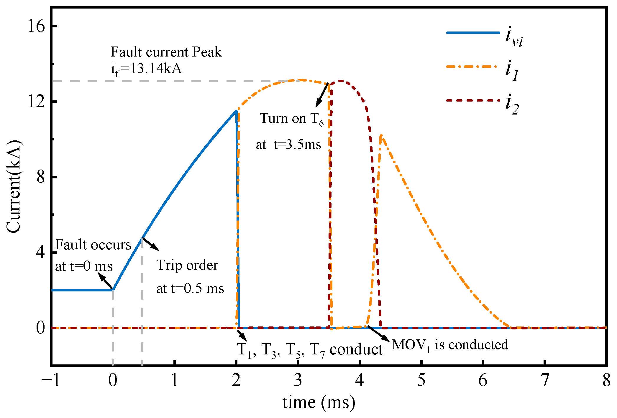
Figure 8.
Simulation results of voltage waveforms for fault current interruption.

Figure 9.
Reliability assessment of interruption. (a) The voltage of VI and the dielectric strength between the contacts. (b) The current change rate of ivi at the moment of the current zero crossing.
Figure 9.
Reliability assessment of interruption. (a) The voltage of VI and the dielectric strength between the contacts. (b) The current change rate of ivi at the moment of the current zero crossing.

Figure 10.
Comparison of current and voltage waveforms between proposed CB and HCB.

Figure 11.
Comparison of energy absorption processes.

Figure 12.
The impact of R1 changes on voltage and energy absorption.

Figure 13.
Four-terminal VSC-HVDC transmission system.

Figure 14.
Performance of short-circuit fault current interruption by B24.

Figure 15.
Performance during reverse direction fault current interruption by B24.

Figure 16.
The voltage equalization circuit of VIs.

Figure 17.
The parameters to be researched.


Table 1.
Parameter value.
| Parameters | Value | |
|---|---|---|
| System voltage | Us | 500 kV |
| Circuit resistance | RS | 20 Ω |
| System inductance | Ldc | 75 mH |
| Load resistance | Rload | 230 Ω |
| Auxiliary capacitor | Cp1 | 10 μF |
| Auxiliary resistance | R2 | 1 kΩ |
| Current-limiting capacitor | Cp | 35 μF |
| Current-limiting resistance | R1 | 50 Ω |
| Coupling coefficient | k | 0.9 |
| Current-limiting inductance | Lp1 | 1 mH |
Table 2.
Comparison between installing and not installing LP.
| Key Parameters | Lp1 = 1 mH | Lp1 = 0 mH |
|---|---|---|
| reverse voltage time of T5 | 190.48 μs | 190.21 μs |
| reverse voltage time of T6 | 456.96 μs | 45.26 μs |
| di/dt of T5 | 288.49 A/μs | 2561.42 A/μs |
| di/dt of T6 | 287.46 A/μs | 2566.96 A/μs |
Table 3.
The maximum du/dt that the thyristor bears during the interruption process.
| T1~T4 | T5 | T6 | T7 | |
|---|---|---|---|---|
| du/dt (V/μs) | 1008.7 | 1645.1 | 662.9 | 1140.8 |
Table 4.
Cost comparison of circuit breakers.
| Index | Proposed HCB (CNY) | Typical HCB (CNY) | Damping HCB (CNY) |
|---|---|---|---|
| MS | 5,500,000 | 5,500,000 | 5,500,000 |
| Capacitor | 5,991,500 | 0 | 4,360,000 |
| Resistor | 588,000 | 0 | 420,000 |
| MICCM | 765,000 | 0 | 850,000 |
| Thyristors and Diodes | 2,790,700 | 0 | 5,280,000 |
| IGBT | 0 | 42,660,000 | 650,000 |
| MOV | 4,160,000 | 5,200,000 | 5,200,000 |
| Total | 19,795,200 | 53,360,000 | 22,260,000 |
Table 5.
Four-terminal VSC-HVDC system parameters.
| Parameter | Converters | |||
|---|---|---|---|---|
| MMC1 | MMC2 | MMC3 | MMC4 | |
| Active power | 2000 MW | 1200 MW | 1600 MW | 1600 MW |
| Reactive power | 0 MVAR | 0 MVAR | 0 MVAR | 0 MVAR |
| Control mode | PV | PQ | PQ | PQ |
| DC voltage | ±500 kV | |||
| Number of submodules | 400 | |||
| Bridge arm capacitance | 22 μF | |||
| Bridge arm inductance | 42 mH | |||
| Bridge arm resistance | 0.08 Ω | |||
| Transformer leakage reactance | 0.18 p.u. | |||
| Ac grids and wind farms | ||||
| Ac grids voltage | 400 kV | |||
| Windfarm output voltage | 66 kV | |||
Disclaimer/Publisher’s Note: The statements, opinions and data contained in all publications are solely those of the individual author(s) and contributor(s) and not of MDPI and/or the editor(s). MDPI and/or the editor(s) disclaim responsibility for any injury to people or property resulting from any ideas, methods, instructions or products referred to in the content. |
© 2024 by the authors. Licensee MDPI, Basel, Switzerland. This article is an open access article distributed under the terms and conditions of the Creative Commons Attribution (CC BY) license (https://creativecommons.org/licenses/by/4.0/).
Share and Cite
MDPI and ACS Style
Liu, S.; Yuan, Z.; Chen, J.; Chen, Y.; Yu, M.; Liu, Z.; Geng, Y. A Cost-Effective Current-Limiting Hybrid DC Circuit Breaker Based on Hybrid Semiconductors. Electronics 2024, 13, 1948. https://doi.org/10.3390/electronics13101948
AMA Style
Liu S, Yuan Z, Chen J, Chen Y, Yu M, Liu Z, Geng Y. A Cost-Effective Current-Limiting Hybrid DC Circuit Breaker Based on Hybrid Semiconductors. Electronics. 2024; 13(10):1948. https://doi.org/10.3390/electronics13101948
Chicago/Turabian StyleLiu, Siyuan, Ziao Yuan, Jinchao Chen, Yifan Chen, Mengze Yu, Zhiyuan Liu, and Yingsan Geng. 2024. "A Cost-Effective Current-Limiting Hybrid DC Circuit Breaker Based on Hybrid Semiconductors" Electronics 13, no. 10: 1948. https://doi.org/10.3390/electronics13101948
Note that from the first issue of 2016, this journal uses article numbers instead of page numbers. See further details here.