Investigation of Ga2O3-Based Deep Ultraviolet Photodetectors Using Plasma-Enhanced Atomic Layer Deposition System


Abstract
:1. Introduction
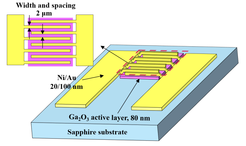
2. Experimental
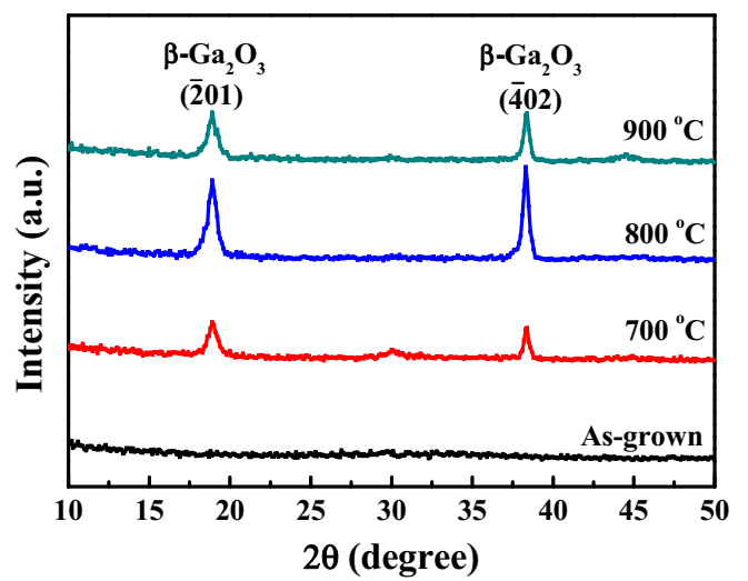
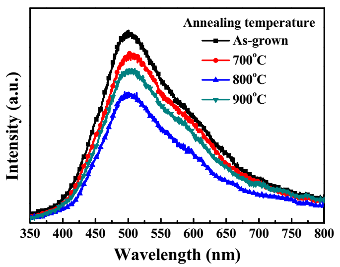
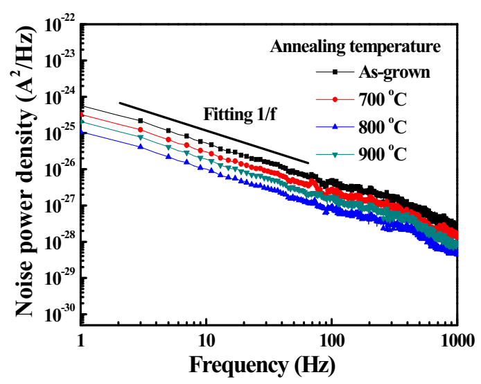
3. Results and Discussion
4. Conclusions
Author Contributions
Funding
Conflicts of Interest
References
- Jheng, J.S.; Wang, C.K.; Chiou, Y.Z.; Chang, S.P.; Chang, S.J. MgZnO/SiO2/ZnO metal-semiconductor-metal dual-band UVA and UVB photodetector with different MgZnO thicknesses by RF magnetron sputter. Jpn. J. Appl. Phys. 2020, 59, SDDF04. [Google Scholar] [CrossRef] [Green Version]
- Wang, H.L.; Liu, J.; Pang, D.R.; Li, T.; Liu, R.H. Mechanisms underlying the protective effects of blueberry extract against ultraviolet radiation in a skin cell co-culture system. J. Funct. Foods 2020, 52, 603–610. [Google Scholar] [CrossRef]
- Kuryatkov, V.; Chandolu, A.; Borisov, B.; Kipshidze, G.; Zhu, K.; Nikishin, S.; Temkin, H.; Holtz, M. Solar-blind ultraviolet photodetectors based on superlattices of AlN/AlGa(In)N. Appl. Phys. Lett. 2003, 82, 1323–1325. [Google Scholar] [CrossRef] [Green Version]
- Ju, Z.G.; Shan, C.X.; Jiang, D.Y.; Zhang, J.Y.; Yao, B.; Zhao, D.X.; Shen, D.Z.; Fan, X.W. MgxZn1−xO-based photodetectors covering the whole solar-blind spectrum range. Appl. Phys. Lett. 2008, 93, 173505. [Google Scholar] [CrossRef]
- Liu, K.W.; Sakurai, M.; Aono, M. ZnO-Based Ultraviolet Photodetectors. Sensors 2010, 10, 8604–8634. [Google Scholar] [CrossRef] [PubMed] [Green Version]
- Wang, J.; Ye, L.J.; Wang, X.; Zhang, H.; Li, L.; Kong, C.Y.; Li, W.J. High transmittance beta-Ga2O3 thin films deposited by magnetron sputtering and post-annealing for solar-blind ultraviolet photodetector. J. Alloys Compd. 2019, 803, 9–15. [Google Scholar] [CrossRef]
- Lee, H.Y.; Liu, J.T.; Lee, C.T. Modulated Al2O3-alloyed Ga2O3 materials and deep ultraviolet photodetectors. IEEE Photon. Technol. Lett. 2018, 30, 549–552. [Google Scholar] [CrossRef]
- Li, X.H.; Detchprohm, T.; Kao, T.T.; Satter, M.M.; Shen, S.C.; Yoder, P.D.; Dupuis, R.D.; Wang, S.; Wei, Y.O.; Xie, H.E.; et al. Low-threshold stimulated emission at 249 nm and 256 nm from AlGaN-based multiple-quantum-well lasers grown on sapphire substrates. Appl. Phys. Lett. 2014, 105, 141106. [Google Scholar] [CrossRef]
- Lee, H.Y.; Wang, M.Y.; Chang, K.J.; Lin, W.J. Ultraviolet photodetector based on MgxZn1-xO thin films deposited by radio frequency magnetron sputtering. IEEE Photon. Technol. Lett. 2008, 20, 2108–2110. [Google Scholar]
- Zhao, D.X.; Liu, Y.C.; Shen, D.Z.; Lu, Y.M.; Zhang, J.Y.; Fan, X.W. Photoluminescence properties of MgxZn1-xO alloy thin films fabricated by the sol-gel deposition method. J. Appl. Phys. 2001, 90, 5561–5563. [Google Scholar] [CrossRef] [Green Version]
- Mastro, M.A.; Kuramata, A.; Calkins, J.; Kim, J.; Ren, F.; Pearton, S.J. Perspective-Opportunities and future directions for Ga2O3. ECS J. Solid State Sci. Technol. 2017, 6, 356–359. [Google Scholar] [CrossRef]
- Pearton, S.J.; Yang, J.; Cary, P.H.; Ren, F.; Kim, J.; Tadjer, M.J.; Mastro, M.A. A review of Ga2O3 materials, processing, and devices. Appl. Phys. Rev. 2018, 5, 011301. [Google Scholar] [CrossRef] [Green Version]
- Zhang, D.; Zheng, W.; Lin, R.C.; Li, T.T.; Zhang, Z.J.; Huang, F. High quality beta-Ga2O3 film grown with N2O for high sensitivity solar-blind-ultraviolet photodetector with fast response speed. J. Alloys Compd. 2018, 735, 150–154. [Google Scholar] [CrossRef]
- Alema, F.; Hertog, B.; Mukhopadhyay, P.; Zhang, Y.; Mauze, A.; Osinsky, A.; Schoenfeld, W.V.; Speck, J.S.; Vogt, T. Solar blind Schottky photodiode based on an MOCVD-grown homoepitaxial β-Ga2O3 thin film. APL Mater. 2019, 7, 022527. [Google Scholar] [CrossRef] [Green Version]
- Zhang, F.; Arita, M.; Wang, X.; Chen, Z.; Saito, K.; Tanaka, T.; Nishio, M.; Motooka, T.; Guo, Q. Toward controlling the carrier density of Si doped Ga2O3 films by pulsed laser deposition. Appl. Phys. Lett. 2016, 109, 100–104. [Google Scholar] [CrossRef]
- Guo, Q.; Nishihagi, K.; Chen, Z.; Saito, K.; Tanaka, T. Characteristics of thulium doped gallium oxide films grown by pulsed laser deposition. Thin Solid Films 2017, 639, 123–126. [Google Scholar] [CrossRef]
- Huang, Y.Q.; An, Y.H.; Wu, Z.P.; Guo, D.Y.; Zhi, Y.S.; Cui, W.; Zhao, X.L.; Tang, W.H. Structural and photoelectrical properties of Ga2O3/SiC/Al2O3 multilayers. J. Alloys Compd. 2017, 717, 8–13. [Google Scholar] [CrossRef]
- Pratiyush, A.S.; Krishnamoorthy, S.; Kumar, S.; Xia, Z.; Muralidharan, R.; Rajan, S.; Nath, D.N. Demonstration of zero bias responsivity in MBE grown β-Ga2O3 lateral deep-UV photodetector. Jpn. J. Appl. Phys. 2018, 57, 060313. [Google Scholar] [CrossRef] [Green Version]
- Kim, J.H.; Holloway, P.H. Microstructural characterization of radio frequency magnetron sputter-deposited Ga2O3: Mn phosphor thin films. J. Vac. Sci. Technol. A 2002, 20, 928–933. [Google Scholar] [CrossRef]
- Li, Z.; An, Z.Y.; Xu, Y.; Cheng, Y.L.; Cheng, Y.N.; Chen, D.Z.; Feng, Q.; Xu, S.R.; Zhang, J.C.; Zhang, C.F.; et al. Improving the production of high-performance solar-blind β-Ga2O3 photodetectors by controlling the growth pressure. J. Mater. Sci. 2019, 54, 10335–10345. [Google Scholar] [CrossRef]
- Dyndal, K.; Zarzycki, A.; Andrysiewicz, W.; Grochala, D.; Marszalek, K.; Rydosz, A. CuO-Ga2O3 Thin Films as a Gas-Sensitive Material for Acetone Detection. Sensors 2020, 20, 3142. [Google Scholar] [CrossRef]
- Lin, C.H.; Lee, C.T. Ga2O3-based solar-blind deep ultraviolet light-emitting diodes. J. Lumin. 2020, 224, 117326. [Google Scholar] [CrossRef]
- Lee, H.Y.; Lin, C.H.; Lee, C.T. Whole metal oxide p-i-n deep ultraviolet light-emitting diodes using i-Ga2O3 active emissive film. IEEE Photon. Technol. Lett. 2020, 32, 941–943. [Google Scholar] [CrossRef]
- Profijt, H.B.; Potts, S.E.; Van De Sanden, M.C.M.; Kessels, W.M.M. Plasma-assisted atomic layer deposition basics opportunities and challenges. J. Vac. Sci. Technol. A 2011, 29, 050801. [Google Scholar] [CrossRef] [Green Version]
- O’Donoghue, R.; Rechmann, J.; Aghaee, M.; Rogalla, D.; Becker, H.W.; Creatore, M.; Wieck, A.D.; Devi, A. Low temperature growth of gallium oxide thin films via plasma enhanced atomic layer deposition. Dalton Trans. 2017, 46, 16551–16561. [Google Scholar] [CrossRef] [PubMed]
- Wei, W.; Qin, Z.X.; Fan, S.F.; Li, Z.W.; Shi, K.; Zhu, Q.S.; Zhang, G.Y. Valence band offset of beta-Ga2O3/wurtzite GaN heterostructure measured by X-ray photoelectron spectroscopy. Nanoscale Res. Lett. 2012, 7, 562. [Google Scholar] [CrossRef] [Green Version]
- Guo, D.; Qin, X.; Lv, M.; Shi, H.; Su, Y.; Yao, G.; Wang, S.; Li, C.; Li, P.; Tang, W. Decrease of oxygen vacancy by Zn-doped for improving solar-blind photoelectric performance in β-Ga2O3 thin films. Electron. Mater. Lett. 2017, 13, 483–488. [Google Scholar] [CrossRef]
- Terasako, T.; Kawasaki, Y.; Yagi, M. Growth and morphology control of beta-Ga2O3 nanostructures by atmospheric-pressure CVD. Thin Solid Films 2016, 620, 23–29. [Google Scholar] [CrossRef]
- Jubu, P.R.; Yam, F.K. Development and characterization of MSM UV photodetector based on gallium oxide nanostructures. Sens. Actuator A-Phys. 2020, 312, 112141. [Google Scholar] [CrossRef]
- Hu, G.C.; Shan, C.X.; Zhang, N.; Jiang, M.M.; Wang, S.P.; Shen, D.Z. High gain Ga2O3 solar-blind photodetectors realized via a carrier multiplication process. Opt. Express 2015, 23, 13554–13561. [Google Scholar] [CrossRef]
- Peng, Y.K.; Zhang, Y.; Chen, Z.W.; Guo, D.Y.; Zhang, X.; Li, P.G.; Wu, Z.P.; Tang, W.H. Arrays of solar-blind ultraviolet photodetector based on beta-Ga2O3 epitaxial thin films. IEEE Photon. Technol. Lett. 2018, 30, 993–996. [Google Scholar] [CrossRef]
- Oh, S.; Kim, C.K.; Kim, J. High responsivity beta-Ga2O3 metal-semiconductor-metal solar-blind photodetectors with ultraviolet transparent graphene electrodes. ACS Photon. 2018, 5, 1123–1128. [Google Scholar] [CrossRef]
- Wu, C.; He, C.; Guo, D.; Zhang, F.; Li, P.; Wang, S.; Liu, A.; Wu, F.; Tang, W. Vertical α/β-Ga2O3 phase junction nanorods array with graphene silver nanowire hybrid conductive electrode for high-performance self-powered solar-blind photodetectors. Mater. Today Phys. 2020, 12, 100193. [Google Scholar] [CrossRef]
- Kumbhar, S.M.; Shaikh, S.K.; Rajpure, K.Y. Hydrothermally-grown TiO2 thin film-based metal-semiconductor-metal UV photodetector. J. Electron. Mater. 2020, 49, 449–509. [Google Scholar] [CrossRef]
- Wang, H.B.; Liu, Q.S.; Wang, X.C.; Yan, J.B.; Tang, H. Ultraviolet photodetector fabricated using laser sintering method grown Mg0.2Zn0.8O film. J. Mater. Sci.-Mater. Electron. 2020, 31, 15659–15668. [Google Scholar] [CrossRef]
- Zheng, M.J.; Gui, P.B.; Wang, X.; Zhang, G.Z.; Wan, J.X.; Zhang, H.; Fang, G.J.; Wu, H.; Lin, Q.Q.; Liu, C. ZnO ultraviolet photodetectors with an extremely high detectivity and short response time. Appl. Surf. Sci. 2019, 481, 422–437. [Google Scholar] [CrossRef]


| Materials and Structure | Photoresponsivity (A/W) | UV/Visible Rejection Ratio | Detectivity (cmHz1/2W−1) | Ref |
|---|---|---|---|---|
| Ga2O3 thin films | 22.19 (at 250 nm) | 5.97 × 10⁴ | 8.74 × 10¹² | This work |
| Ga2O3 nanostructures | 38.161 (at 365 nm) | – | 8.39 × 10⁹ | [29] |
| Ga2O3 thin films | 17 (at 255 nm) | 8.5 × 10⁶ | 7.00 × 10¹² | [30] |
| Ga2O3 thin films | 0.893 (at 250 nm) | 9.75 × 10² | – | [31] |
| Ga2O3 thin films | 29.8 (at 254 nm) | 9.4 × 10³ | 1.00 × 10¹² | [32] |
| α/β-Ga2O3 nanorods | 0.00026 (at 254 nm) | 2.7 × 10³ | 2.8 × 10⁹ | [33] |
| TiO2 thin films | 13.29 (at 365 nm) | – | 4.91 × 10¹³ | [34] |
| MgZnO thin films | 0.14 (at 325 nm) | 3.83 × 10³ | 4.42 × 10¹² | [35] |
| ZnO thin films | 27 (at 365 nm) | – | 8.5×10¹³ | [36] |
Publisher’s Note: MDPI stays neutral with regard to jurisdictional claims in published maps and institutional affiliations. |
© 2020 by the authors. Licensee MDPI, Basel, Switzerland. This article is an open access article distributed under the terms and conditions of the Creative Commons Attribution (CC BY) license (http://creativecommons.org/licenses/by/4.0/).
Share and Cite
Chu, S.-Y.; Shen, M.-X.; Yeh, T.-H.; Chen, C.-H.; Lee, C.-T.; Lee, H.-Y. Investigation of Ga2O3-Based Deep Ultraviolet Photodetectors Using Plasma-Enhanced Atomic Layer Deposition System. Sensors 2020, 20, 6159. https://doi.org/10.3390/s20216159
Chu S-Y, Shen M-X, Yeh T-H, Chen C-H, Lee C-T, Lee H-Y. Investigation of Ga2O3-Based Deep Ultraviolet Photodetectors Using Plasma-Enhanced Atomic Layer Deposition System. Sensors. 2020; 20(21):6159. https://doi.org/10.3390/s20216159
Chicago/Turabian StyleChu, Shao-Yu, Meng-Xian Shen, Tsung-Han Yeh, Chia-Hsun Chen, Ching-Ting Lee, and Hsin-Ying Lee. 2020. "Investigation of Ga2O3-Based Deep Ultraviolet Photodetectors Using Plasma-Enhanced Atomic Layer Deposition System" Sensors 20, no. 21: 6159. https://doi.org/10.3390/s20216159