Observations of Partial Discharge Echo in Dielectric Void by Applying a Voltage Chopped Sequence


ABB Corporate Research, ul.Starowiślna 13A, 31-038 Kraków, Poland
Energies 2018, 11(10), 2518; https://doi.org/10.3390/en11102518
Submission received: 27 August 2018
/
Revised: 17 September 2018
/
Accepted: 19 September 2018
/
Published: 21 September 2018
Abstract
:This paper describes a novel observation on partial discharges (PDs), which occur despite the absence of an applied voltage, within a chopped sequence. It was found that additional discharge pulses occur when a specimen is subjected to chopped sequences rather than a continuous sinusoid. The discharge pulses, called Partial Discharge Echoes (PDE), appeared in time intervals (where no voltage was being applied), immediately after the specimen had been exposed to a base waveform (e.g., sinusoidal) above a partial discharge inception level. The chopped timing is composed of a multiple series of packets consisting of base waveforms, with each packet being separated in time by a defined delay period. The presented experiments were performed on specimens with an embedded gaseous void, in thermosetting insulation and glass as a non-polar material, for comparison. Acquisition of the echo signal was performed in the phase-resolved mode, modifying the synchronization path and the settings. In contrast to continuous sinusoidal PD measurements, the chopped approach might provide a deeper insight into key PD phenomena, such as inception, propagation, time lag, post-discharge time decay, and effective surface area. Special focus was paid to the transition point between sinusoidal phase and the echo interval. The various scenarios of an echo mechanism, depending on the coincidence of remnant polarization field and the field accumulated on void walls, are discussed.
1. Introduction
Partial discharges (PDs) being one of the main assessment indicators of high-voltage insulation integrity, still offer a potential for new approaches in detection, mechanism interpretation, and analysis. This paper describes a novel observation related to partial discharges which occur despite the absence of an applied voltage, within a chopped sequence. The discharge pulses, called Partial Discharge Echoes (PDE), appeared in time intervals where no voltage was being applied, immediately after the specimen had been exposed to a base waveform (for example sinusoidal) voltage above the partial discharge inception level.
The chopped PD sequence opens new opportunities for analysis of dynamic phenomena inside dielectric materials, such as charge accumulation, the build-up of an internal field, including the role of the remnant field (due to dielectric polarization) that remains after the external voltage has been removed, space charge, time lag, as well as the processes of charge decay, related to the surface material conductivity [1,2]. The chopped timing is composed of a multiple series of packets consisting of base waveforms, with each packet being separated in time by a defined delay period. Whole epochs are repeated periodically throughout the measurement period [1]. The presented experiments were performed on specimens with an embedded gaseous void in thermosetting insulation, and glass as a non-polar material for reference. In polar dielectrics, the remnant electric field plays an important role within the PD Echo voltage-less period. Additionally, the purpose of this paper is to analyze various scenarios of PDE mechanism, including multiple PD Echo (dependent on the coincidence of remnant polarization field), and the accumulated field from previous discharges, which is completely new with respect to the echo phenomena and have not been published before this.
Comparison of the PD, in polar and non-polar dielectric material, was also performed around the transition point from the high-voltage driven phase to the chopped period. The occurrence of discharges in this phase range requires special attention since they impact the PD Echo mechanism and the timing.
Acquisition of the echo signal was carried-out in a phase-resolved mode, modifying the synchronization path and the settings. The controlled high-voltage source could be implemented with Trek HV amplifier. In contrast to the continuous sinusoidal PD measurements, the chopped approach may provide deeper insight to key PD phenomena, such as inception, propagation, time lag, neutralization, post-discharge time decay, effective surface area, etc. [3,4,5,6,7,8,9,10,11,12,13,14,15,16,17,18,19,20].
This paper contains examples of the PD echo obtained in specimens composed of a void, in both a thermosetting material and in glass. The various events of echo mechanism, such as late (even tens of milliseconds after transition point) or multiple echoes, resulting from the interplay of remnant polarization field and accumulated field, have been discussed.
2. Partial Discharge Echo in Chopped Sequence
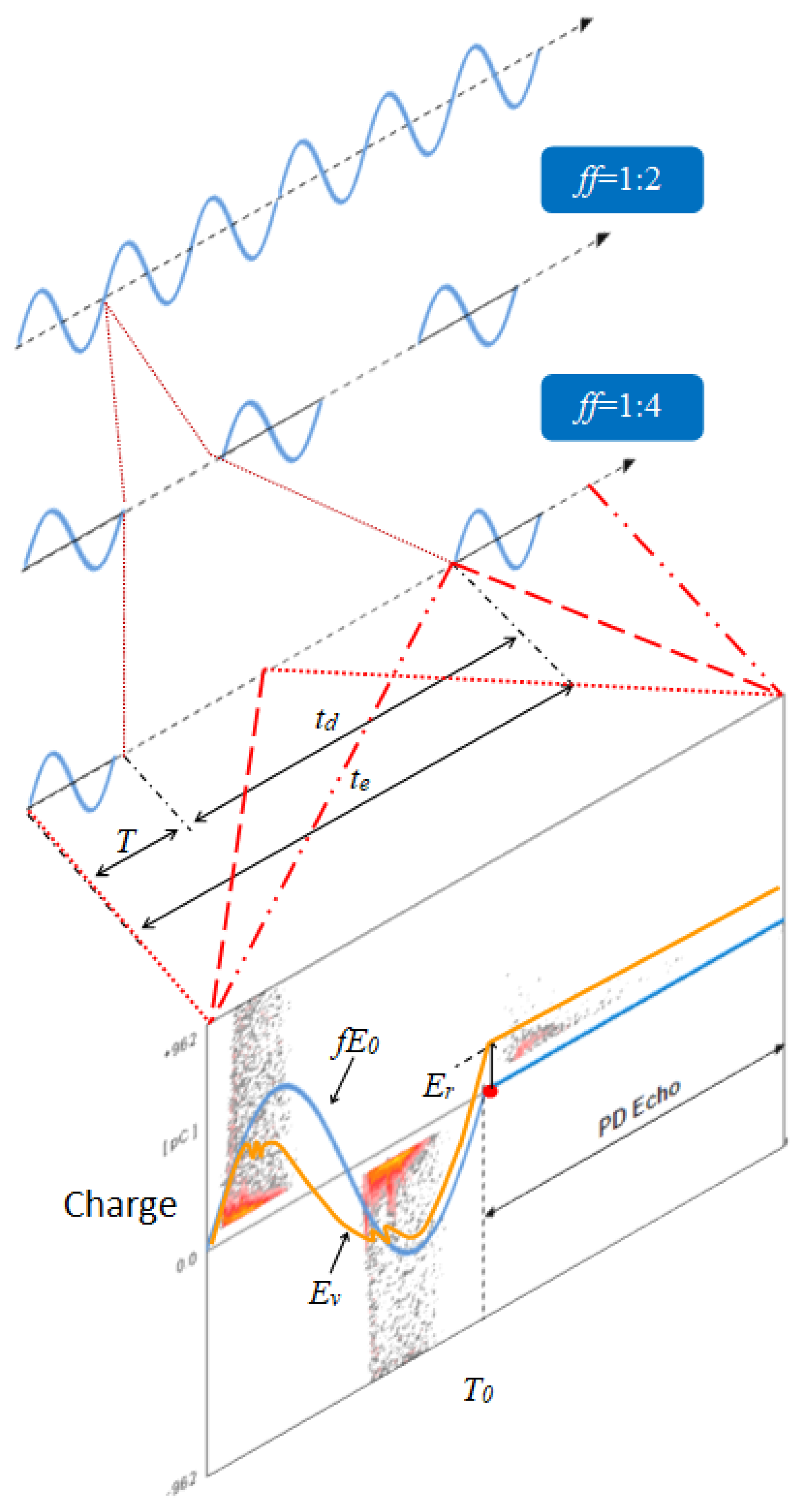
By applying a chopped sequence, aspects of the partial discharge process, not measurable via traditional methods, might be observed. An illustration of a chopped sequence is given in Figure 1. In contrast to a standard continuous sinusoidal run, a discontinuous approach is characterized by time intervals of duration td where no voltage is applied [1]. The base waveform with a period T (sinusoidal in the presented experiments, however, other shapes of a base waveform may also be applied) and the time delay, together form an epoch lasting for time te. Each epoch may contain multiple base packets. The proportion of the duration of active waveforms to the duration of the whole epoch is called the fill factor ff. The transition point from the sinusoidal part to the echo interval is extremely important and denoted as T0 (red dot), in Figure 1. For clarity, the time interval, between consecutive sinusoidal periods is denoted in the patterns, in time units, in contrast to the phase units of the sinusoidal part [21].
Dielectric properties are determined by free and bounded charges. Free charges in the form of ions and carriers can move in the electric field. The mobility, whilst very small, is sufficient to observe the current flow, which is measured by the conductivity. Bounded charges are defined by the polar groups of atoms found in the main and the side chains of the polymer. These groups can rotate in the applied external electric field, which is equivalent to the flow of electric current, called displacement in the dielectric. In the electric field, dipoles subject a partial orientation that is the result of the equilibrium of the orientation, and a focusing on the external field, as well as, the confusing influence of thermasl movements. The relaxation time between different solid dielectric materials differs by a few orders of magnitude [22]. The effective electric field inside the void Ev is a superposition of applied external field E0 (corresponding to the test voltage), which is transposed according to the field distribution and the shape of the void, by the factor f, and the internal field Eq, created by the charges accumulated on the void surface, during a previous discharge event:
where τq represents the cumulative decay time constant of the Eq field in the void, due to surface recombination, deeper trapping, and bulk conduction, neutralization, and other drifts. The Eq field can be expressed as a decaying function of time:
where Eq0 is the initial field value.
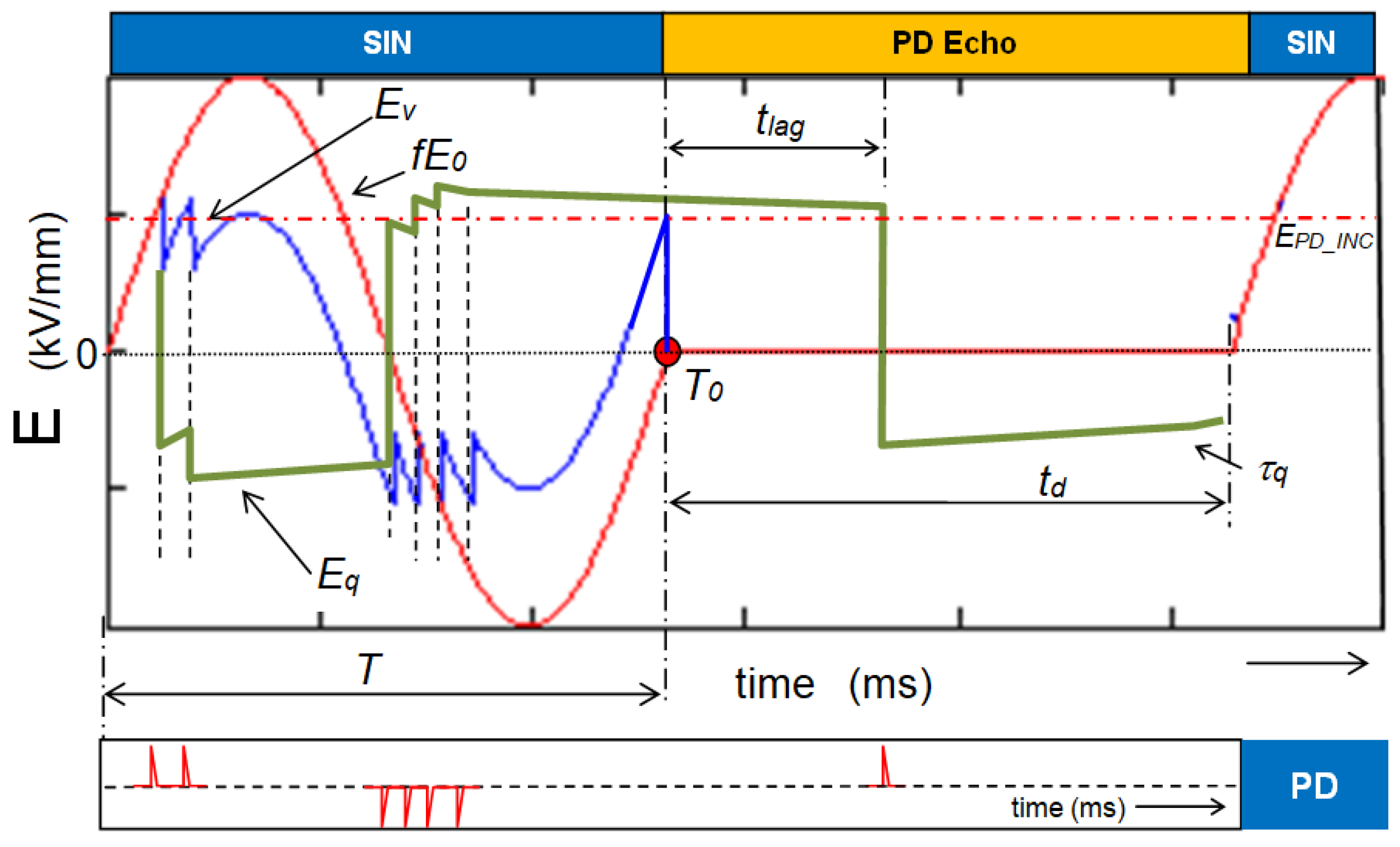
As illustrated in Figure 1, at the transition moment T0, at the beginning of the echo part, there would be a “quasi-DC” remnant field Er, present in the void, due to the capacitive polarization of the dielectric Ep, superimposed with the charge accumulated Eq field (Figure 2a). Hence, in the echo interval, Er would coexist with the decaying Eq field, as shown in Figure 2b, assuming there is a much slower decay of the polarization field Ep. As a result, both Er and Eq fields would be present in the voltage-less time interval, due to the fact that the driving field fE0 will stop abruptly at the transition point T0. In addition, the Er field is related to polar dielectrics. After transition moment T0, the void field would be a superposition of the remnant field and the accumulated field, taking into account their polarity:
where function polEq controls the polarity of Eq field at PD events.
A demonstrative illustration of this situation is presented in Figure 2a. Just before the transition T0−, the polarization field Ep, based on the fE0 but phase-shifted due to the discharges, would polarize and positively orient the dipoles in the dielectric. This is indicated by the yellow waveform, in Figure 1 (the void field “frozen” as a remnant, quasi-DC field, is also marked in the chopped part, where the PDE signal appears).
Hence at T0+, the void sees the remaining field that is memorized in dipoles and the field from the accumulated past events, which have compatible directions only once, after the polarity reversal (marked by a red arrow in Figure 2b). The remnant field, except for the depolarization, is quasi-stable. After the first discharge, the directions of the Er and Eq field are opposite to each other, thus, Eq is a weakening remnant field. However, a post-discharge decay of the accumulated field Eq leads to the restoration, and an increase, of the resultant field, until a subsequent discharge event occurs, as is illustrated in Figure 2b. The various scenarios and polarizations of this field are analyzed in Section 5 of this paper. The presented experiments were carried out on a void, in a thermosetting material and, for comparison of non-polar behavior, on a void encapsulated in glass.
3. Measurement Setup and Dielectric Specimens
The experimental setup for a PD Echo measurement in a phase-resolved mode is presented in Figure 3a. The partial discharge signal was detected using a measuring impedance Zm, connected in series with a coupling capacitor Ck = 1100 pF, then filtered and preamplified in the signal-conditioning unit SCU (signal conditioning unit and preamplifier). The acquisition was synchronized with the zero phase angle of the testing voltage and discharge pulses were accumulated, in a 256 × 256 matrix, in an ICM system (Power Diagnostix, Germany) connected to a host computer via GPIB (General Purpose Interface Bus) bus, during a tm = 60 s measurement period. Thus, for the base period equal to T = 20 ms (50 Hz), the total number of periods, within the measuring time tm, was 3000. Depending on the fill factor in the chopped sequence, the number of active periods would be reduced accordingly.
The main difference in instrumentation and acquisition of the chopped patterns was related to the necessity of a high-voltage source and synchronization modes. The measurements were performed in a phase-resolved, wideband PD acquisition system. The chopped pattern was defined in a waveform generator driving the Trek Model 20/20B (Trek Inc., New York, NY, USA) high-voltage amplifier. The period of the sinusoidal base waveform was 20 ms. The synchronization was obtained from a compensated voltage divider connected to a high-voltage terminal. The measurement time for all experiments presented in this paper was 60 seconds. Partial discharge detection was provided from coupling impedance, followed by a filter and a preamplifier. The PD pattern including the echo was stored in a 256 × 256 matrix.
Following the frequency of the base waveform, at 50 Hz, the synchronization was adjusted to 25 Hz to visualize both the PD sinusoidal part and the echo interval. The position-ing of an acquisition window is illustrated in Figure 3b. The two synchronization frequencies fV and fS are also marked. The first 128 channels in the acquisition matrix were devoted to recording the sinusoidal excitation and the remaining 128 channels were dedicated to recording the PD echoes [1,2].
One specimen contained an artificial void filled with air at atmospheric pressure. The thermosetting embedded void had a radius of 15 mm and a thickness of 0.1 mm. The thermosetting material was a composition of mica, estrofol foil, and epoxy resin. For comparison, a void (radius 15 mm, thickness 0.1 mm) placed between the two glass plates, each 2 mm thick, was used. On both sides, plain stainless steel electrodes were used. The electrodes were 40 mm in diameter, with an end curvature of 8 mm radius. During the experiments, the specimen was placed in an oil tank. Furthermore, the measurements were performed at room temperature.
4. Results and Discussion
4.1. Chopped Sequence
The application of the chopped sequences to the specimen, resulted in additional observations when a continuous sinusoid was applied. The following two configurations were considered; the first refers to the void embedded in the glass and the second to when the void was embedded in thermosetting insulation. Glass was selected as a non-polar, electrically insulating material, for comparison. In the 17th century, it was already in use, as an insulation material in the Leyden jar, and later, for example, it was used in glass capacitors introduced by Prof. Mościcki [23]. Glass is made of SiO2 molecules. Oxygen has a high affinity for attracting electrons of other atoms. In this case, after a discharge event, electrons on one void wall created relatively stable negative ions. In the non-polar glass, the polarization field was not present. Figure 4 shows the PD phase-resolved measurements obtained in the case of a continuous (Figure 4a) and a chopped sequence, in a void embedded in glass, at a voltage of 7.5 kV, which equaled to 1.2 U0 (U0 is the PD inception voltage). The non-continuous part reflected measurement at the delay times of 40 ms and 320 ms, corresponding respectively, to a fill factor of 1:2 and 1:16.
Initially, no phase shifts of PD groups could be observed between the continuous and the chopped (ff = 1:2) sequence. Thus, both positive and negative discharge groups were stable, despite the introduced 20 ms delay, after the first period of high-voltage. It might be observed that both the continuous sinusoidal and the chopped patterns were invariant. This confirmed that the Eq field created by the post-discharges on the void walls was stable (Δϕ(td) = 0), in this case; no decay was observed. However, when the delay time was prolonged to 320 ms, the decay effect of Eq (e.g., due to surface processes) emerged in the form of a phase-shift, by 10°, of the positive PD group (Figure 4b vs. Figure 4c). The maximum charge Qmax was stable and was not influenced by the delay time in both PD groups.
For comparison, a second experiment was performed on a void embedded in a thermosetting material, at a voltage of 7.5 kV (Figure 5). Contrary to the glass void, in this case, significant differences might be observed between the PD pattern obtained in the case of chopped sequence and that which was obtained for the continuous run. It was evident that the introduced gap in the form of the predefined delay time had impacted the PD inception voltage, of the first period, in the sequence.
The inception phase had shifted to the right, from 20° to 35°, and the maximum charge magnitude of the PD pulses had increased, greatly, from 0.7 to 1.8 nC. A shift of the positive discharge group might be noted, which was related to a slightly higher inception voltage, that was used to for compensate the loss of internal Eq field. This quite significant increase in the front pattern in the maximum charge, after the delay time, reflected the incoming overvoltage, which might be a result of the decay of Eq, as well as a decrease of the remnant polarization field Er.
4.2. Partial Discharge Echo
The application of the chopped sequence led to the additional observation of the partial discharge echo phenomena in the voltage-less time interval. The PD pattern was recorded in the chopped sequence with the delay time td = 20 ms (ff = 1:2), in void embedded in glass, at 7.5 kV 1.2 U0 (Figure 6a), and with PDE at 2.4 U0, as is shown in Figure 6b. It could be observed from these patterns that PD Echo appears at a significantly high-voltage of 15 kV, which is equal to 2.4 U0. This could be attributed to a lack of remnant field. From previous observations, it could be stated that the echo effect started to appear in various dielectric specimens at voltage levels around 1.2 U0. However, with glass, which was the non-polar specimen, it was not the case and the echo started at a higher voltage. In Figure 7b, the characteristic phase shift towards left might be observed, in the positive PD group, with the classic split into two parts, one in the positive half-period and the second seen at the end of the negative period. These PD pulses have a positive polarity, due to the internal phase shift in the dielectric material, between the external field and the internal void field, in the presence of discharges.
An interesting result may be observed around the transition point T0. Prior to the polarity change of the external voltage and the transition point T0, there was already a group of partial discharge pulses, which could be considered to be a classical PD. However, these classical pulses also had a significant impact on the echo mechanism. Following T0, there was a long spread of the PDE pulses, almost over the entire 20 ms-long delay-period.
In the case of the void in the thermosetting insulation, the corresponding PDE patterns are presented in Figure 7. A non-continuous sequence with a delay time of 160 ms (ff = 1:4) was presented. The PD Echo started to appear at voltage 11 kV, equal to 1.7 U0 (Figure 7a). By further increasing the voltage, one could identify a more focused PDE group and a strong increase in the maximum charge (Figure 7b). At lower voltages, echo pulses started, individually, in the voltage-less part. By further increasing the voltage, the positive group just prior to the transition point T0 arose, which had an impact on the subsequent PD development. These two mechanisms are explained in the next section.
5. Selected Scenarios of PD Echo Mechanism
Depending on the dielectric material (polar/non-polar) and the interplay of the remnant Er field with the field from accumulated charges Eq, inside the void, various PD Echo scenarios could be considered. Additionally, the time lag was also taken into account. This could last from hundreds of milliseconds for the low frequency (1 Hz), to individual milliseconds at a power frequency of 50/60 Hz [2,24,25].
The internal remnant field Er was obtained due to the polarization effect of the external field, in a polar dielectric. The dipoles were oriented partly along the field as an effect of the balance of orienting the action of the external electric field and disorienting the effect of thermal movements. Due to the voltage-less part of the sequence, the dipoles returned to a statistical average of disordered placement (the equilibrium state), which is usually described as an exponential relaxation process (in solid dielectrics, in the range 10−4–104 second) [18,23]. In the presented experiments, the Er relaxation time in a solid dielectric was assumed to be long, relative to the high-voltage period. The PD pulses, prior to the transition point T0 and the PD Echo pulses in the voltage-less part, were observed in both cases of the void being embedded in glass and that of it being embedded in the thermosetting insulation. Following is an explanation of the potential mechanisms and scenarios for this behavior, depending on the presence and interactions of the remnant and the accumulated internal field, in the void.
First, consider the case, visualized in Figure 8a, where an individual PDE pulse was recorded. This PD echo impulse was triggered due to the coinciding of both Er and Eq fields, after passing the inception level. The time delay was due to the time lag (Figure 8a). The Eq accumulated field is represented by a green curve in Figure 8b, and the field inside the void is given in blue.
In the sinusoidal phase, the PDE mechanism was related to the difference of the external and the accumulated field, whereas, in the echo interval it was primarily related to the remnant field. The waveforms of the corresponding electric field components are shown in Figure 8b. Visualization in the plot has not been done to scale, to pinpoint the discharge mechanism.
Cases where multiple echo pulses followed each other in a sequence, were also observed, as shown in Figure 9a. In this case, after the first PDE pulse, as described above, the second one would be triggered, when the following condition was full filed: Er − Eq > EPD_INC. After the first PDE pulse, the Eq field had an opposite direction to the Er field counteraction. Eq field was found to decay with the time constant τq, as indicated in Figure 9b, and the moment when superposition of those fields exceeded the inception level (marked by a red dot in Figure 9b), the subsequent echo pulse appeared. This was called a “late” echo, because it was observed often after tens of milliseconds, from the transition point T0, depending on the decay time constant of the Eq field. The visualization of this process is shown in Figure 2b. In a positive polarity sequence, the PD Echo pulses also had a positive polarity. Thus, the second PDE pulse must have been caused by the Er field as the Eq field had flipped, and hence would result in a negative PDE, which was not observed.
Another scenario refers to the case when prior to the transition point T0, PD pulses occur at the end of the sinusoidal part. Here we can distinguish between the two cases observed in our experiments for polar dielectric (thermosetting specimen) and non-polar material (glass specimen).
First consider the case with a polar dielectric, where the remnant field Er was maintained. A time snapshot of such an instance is shown in Figure 10a, where three partial discharge echo pulses with positive polarity could be recognized. Prior to the transition moment T0, the internal conditions in the void acted to support the discharge event (sufficient Er + Eq field above inception threshold, initial electron available). After the first discharge Eq, the field would flip, being in opposition to Er for subsequent events. Hence at T0, the remnant field was frozen and Eq had weakened the internal field in the void. The decaying accumulated field would restore the void field, as previously described, and the trigger the event in the case of the fulfilling discharge criteria. Depending on the Eq field decay time τq, multiple PDE pulses might have occurred. This time constant could have different origins such as ionic drift, neutralization, conduction along the void surface and recombination, and trapping into the dielectric or bulk conduction. Depending on the trapping level, some electrons might have been de-trapped, in this process, for a subsequent discharge. It should be noticed that in the presented scenarios it was assumed that the Eq field had always changed its polarity after the first discharge, when both Er and Eq were coherent. One could imagine a situation, where the accumulated field was substantial and one discharge event was not able to change the polarity. In such a situation the process would be more gradual.
Now consider the PD echo observed in the glass specimen (Figure 6b) where discharges, both prior to T0 and in the echo time interval, are recorded. In the case of non-polar dielectric, the PDE pulses were obtained at relatively high multiples of the PD inception voltage, for sinusoidal voltage (2.4 U0), as the remnant field Er, supporting the Eq field in the case of the first discharge after polarity reverse, was not present. This case could be split into two parts. The group before T0 could be formed in a regular sinusoidal sequence, especially when the voltage was high, with respect to the inception level.
This did not address the question of how the echo pulses were generated. Since glass is a non-polar insulating material, no remnant electric field remained after T0.
The observed echo pulses had a positive polarity, thus, they could not have been caused by a flipping of the Eq field. The intensity of the PDE versus prior T0 discharges, whilst relatively low, was still significant and observable. Thus, a possible explanation (illustrated in Figure 11) might relate to the scenario when no prior T0 discharges had happened, in some sequences, and there was an accumulated Eq field, including in the time lag condition, as this would have resulted in an intermittent echo discharges, spread along the entire delay time interval. However, in this case, less probable was the occurrence of multiple echoes in a single sequence. The measurement observation recorded in Figure 6b supported this hypothesis, as the partial discharge echo pulses covered the delay time period td. The mechanism visualized in Figure 11, also shows the interplay of the two effects, i.e., first related to the time lag and the electron availability, and the second one associated with the decay of the Eq field.
6. Conclusions
This paper reported a novel observation on partial discharges, which occurred despite the absence of an applied voltage, within a chopped sequence. The chopped sequence allowed to separate the consecutive periods of high-voltage and provide insight into the physical PD mechanism. The Partial Discharge Echoes pulses were recorded in the chopped sequence in time intervals where no voltage was applied. Experiments were performed on specimens with an embedded gaseous void in the thermosetting insulation and glass. They demonstrated a comparison of both the chopped effect and the PD Echo, in polar versus non-polar dielectric material, revealing the impact of a remnant field.
Various scenarios of PDE mechanisms, including multiple PD Echo, were analyzed, depending on the coinciding of the remnant polarization field (present only in polar dielectrics) and the field accumulated from previous discharges, which is a novel observation in the echo phenomena. It was shown that in the sinusoidal phase, the PD mechanism was related to the difference of external and accumulated field, whereas, in the PDE interval it was primarily related to the remnant field and accumulated field for polar dielectrics, and only to Eq field, in the case of non-polar insulating materials. In the case of polar dielectrics, multiple echo pulses were observed. A “late” echo, occurring after tens of milliseconds from the transition point was also observed. For the above-mentioned effects, the corresponding PD mechanisms and the interplay of electric fields, in the void, was explained and visualized.
It was detected that the PD pulses occurring just prior to the transition point T0 influenced the PD Echo occurrence and timing. Acquisition of PDE was demonstrated and a mechanism based on the superposition of a remnant polarization field, and an accumulated internal field, was explained.
In contrast to the continuous sinusoidal PD measurements, the chopped approach might provide deeper insight into key PD phenomena, such as inception, propagation, time lag, post-discharge time decay, and effective surface area. Special focus was paid to the transition point between the sinusoidal phase and the echo interval. The various scenarios of echo mechanisms, depending on the coinciding of the remnant polarization field and the accumulated field, on void walls, were analyzed and explained. The preliminary PD echo observations confirmed a high potential for research into its interpretation, further analysis, and application.
Conflicts of Interest
The author declares no conflict of interest.
References
- Florkowski, M.; Florkowska, B.; Zydron, P. Chopped Partial Discharge Sequence. IEEE Trans. Dielectr. Electr. Insul. 2015, 22, 3451–3458. [Google Scholar] [CrossRef]
- Florkowski, M.; Florkowska, B.; Zydron, P. Partial discharge echo obtained by chopped sequence. IEEE Trans. Dielectr. Electr. Insul. 2016, 23, 1294–1302. [Google Scholar] [CrossRef]
- Tanaka, T.; Ikeda, Y. Internal Discharges in Polyethylene with an Artifical Cavity. IEEE Trans. Power Appl. Syst. 1971, 90, 2692–2702. [Google Scholar] [CrossRef]
- Crichton, G.C.; Karlsson, A.; Pedersen, A. Partial discharges in ellipsoidal and spheroidal voids. IEEE Trans. Electr. Insul. 1984, 24, 335–342. [Google Scholar] [CrossRef] [Green Version]
- McAllister, I.W. Decay of charge deposited on the wall of gaseous void. IEEE Trans. Electr. Insul. 1992, 27, 1202–1207. [Google Scholar] [CrossRef] [Green Version]
- Niemeyer, L. A generalized approach to partial discharge modeling. IEEE Trans. Dielectr. Electr. Insul. 1995, 2, 510–528. [Google Scholar] [CrossRef]
- Florkowski, M.; Florkowska, B. Distortion of partial-discharge images caused by high-voltage harmonics. IEE Proc. Gener. Transm. Distrib. 2006, 153, 171–180. [Google Scholar] [CrossRef]
- Holboll, J.T.; Henriksen, M. Partial discharge patterns and surface deterioration in voids in filled and unfilled epoxy. In Proceedings of the Conference Record of the 1992 IEEE International Symposium on Electrical Insulation, Baltimore, MD, USA, 7–10 June 1992; pp. 354–358. [Google Scholar] [Green Version]
- Gutfleisch, F.; Niemeyer, L. Measurement and simulation of PD in epoxy voids. IEEE Trans. Dielectr. Electr. Insul. 1995, 2, 729–743. [Google Scholar] [CrossRef]
- Zhang, X.; Zhang, G.; Li, Y.; Zhang, J.; Huang, R. On the Feasibility of Gap Detection of Power Transformer Partial Discharge UHF Signals: Gap Propagation Characteristics of Electromagnetic Waves. Energies 2017, 10, 1531. [Google Scholar] [CrossRef]
- Tanaka, T.; Uchiumi, M. Two kinds of decay time constants for interfacial space charge in polyethylene-laminated dielectrics. In Proceedings of the 1999 Annual Report Conference on Electrical Insulation and Dielectric Phenomena (Cat. No. 99CH36319), Austin, TX, USA, 17–20 October 1999; pp. 472–475. [Google Scholar]
- Jiang, J.; Zhao, M.; Zhang, C.; Chen, M.; Liu, H.; Albarracín, R. Partial Discharge Analysis in High-Frequency Transformer Based on High-Frequency Current Transducer. Energies 2018, 11, 1997. [Google Scholar] [CrossRef]
- Li, X.; Wang, X.; Xie, D.; Wang, X.; Yang, A.; Rong, M. Time–frequency analysis of PD-induced UHF signal in GIS and feature extraction using invariant moments. IET Sci. Meas. Technol. 2018, 12, 169–175. [Google Scholar] [CrossRef]
- Li, S.; Gao, G.; Hu, G.; Gao, B.; Yin, H.; Wei, W.; Wu, G. Influences of Traction Load Shock on Artificial Partial Discharge Faults within Traction Transformer—Experimental Test for Pattern Recognition. Energies 2017, 10, 1556. [Google Scholar] [Green Version]
- Mizutani, T.; Taniguchi, Y.; Ishioka, M. Charge decay and space charge in corona-charged LDPE. In Proceedings of the 11th International Symposium on Electrets, Melbourne, Victoria, Australia, 1–3 October 2002; pp. 15–18. [Google Scholar]
- Sadaoui, F.; Beroual, A. AC creeping discharges propagating over solid–gas interfaces. IET Sci. Meas. Technol. 2014, 8, 595–600. [Google Scholar] [CrossRef]
- Wu, K.; Ijichi, T.; Kato, T.; Suzuoki, Y.; Komori, F.; Okamoto, T. Contribution of surface conductivity to the current forms of partial discharges in voids. IEEE Trans. Dielectr. Electri. Insul. 2005, 12, 1116–1124. [Google Scholar]
- Illias, H.; Chen, G.; Lewin, P. Partial Discharge within a spherical cavity in a dielectric material as a function of cavity size and material temperature. IET Sci. Meas. Technol. 2012, 6, 52–62. [Google Scholar] [CrossRef]
- Kumara, S.; Serdyuk, Y.V.; Gubanski, S.M. Surface charge decay on polymeric materials under different neutralization modes in air. IEEE Trans. Dielectr. Electr. Insul. 2011, 18, 1779–1788. [Google Scholar] [CrossRef]
- Moonesan, M.S.; Jayaram, S.H.; Cherney, E.A. Impact of Charge Accumulation on Insulation Films Subjected to Unipolar and Bipolar Square Waves. IEEE Trans. Dielectr. Electr. Insul. 2017, 24, 2626–2632. [Google Scholar] [CrossRef]
- Florkowski, M.; Florkowska, B.; Włodek, R. Investigations on post partial discharge charge decay in void using chopped sequence. IEEE Trans. Electr. Insul. 2017, 24, 3831–3838. [Google Scholar] [CrossRef]
- Dissado, L.A.; Fothergill, J.C. Electrical Degradation and Breakdown in Polymers; IET Institution Engineering and Technology: London, UK, 1992. [Google Scholar]
- Drewnowski, K. Mościcki electric capacitors and their application. Przegląd Techniczny 1911, 4, 48–50. [Google Scholar]
- Devins, J.C. Current pulse shapes of discharges in air gaps limited by series dielectrics. In Proceedings of the IEEE Conference on Electrical Insulation, Linden, NJ, USA, 21–23 Ocotober 1957; 6–11; pp. 6–11. [Google Scholar]
- Illias, H.A.; Tunio, M.A.; Mokhlis, H.; Chen, G.; Bakar, A.H.A. Determination of partial discharge time lag in void using physical model approach. IEEE Trans. Dielectr. Electr. Insul. 2015, 22, 463–471. [Google Scholar] [CrossRef]
Figure 1.
Illustration of a chopped partial discharge methodology, T—period of a base waveform, td—delay time, te—duration of the epoch, fE0—transposition of the external field, Er—remnant field, Ev—field in the void. PD: Partial discharge.
Figure 1.
Illustration of a chopped partial discharge methodology, T—period of a base waveform, td—delay time, te—duration of the epoch, fE0—transposition of the external field, Er—remnant field, Ev—field in the void. PD: Partial discharge.

Figure 2.
Interplay of electric fields in a void. (a) Illustration of the void stress at the transition point T0, being the superposition of polarization, and Eq field (illustration for a case when no PDs are present, just before the T0 in the sinusoidal part), (b) visualization of the remnant and accumulated field dynamic.

Figure 3.
Partial discharge echo acquisition methodology using chopped sequence (a) experimental setup in a phase-resolved mode, R1, R2—resistive divider (1000:1), Cx—specimen, Ck—coupling capacitor (1100 pF), Zm—measuring impedance, SCU—signal conditioning unit and preamplifier, Z—protection and filtering impedance; (b) illustration of acquisition window positioning and synchronization.


Figure 4.
Partial discharges (PD) pattern obtained at (a) continuous sinusoidal voltage (td = 0 ms), at 7.5 kV, in void embedded in glass, and in a chopped PD sequence (b) 1:2, (td = 40 ms), (c) 1:16 (td = 320 ms).
Figure 4.
Partial discharges (PD) pattern obtained at (a) continuous sinusoidal voltage (td = 0 ms), at 7.5 kV, in void embedded in glass, and in a chopped PD sequence (b) 1:2, (td = 40 ms), (c) 1:16 (td = 320 ms).


Figure 5.
PD pattern obtained at (a) continuous sinusoidal voltage (td = 0 ms), at 7.5 kV, in void, embedded in a thermosetting material, and in the chopped PD sequence; (b) 1:2; (td = 40 ms).
Figure 5.
PD pattern obtained at (a) continuous sinusoidal voltage (td = 0 ms), at 7.5 kV, in void, embedded in a thermosetting material, and in the chopped PD sequence; (b) 1:2; (td = 40 ms).

Figure 6.
The PD pattern recorded in the chopped sequence with the introduced delay time td = 20 ms (ff = 1:2), in void embedded in glass, at (a) 7.5 kV 1.2 U0, and (b) with PD Echo at 2.4 U0.
Figure 6.
The PD pattern recorded in the chopped sequence with the introduced delay time td = 20 ms (ff = 1:2), in void embedded in glass, at (a) 7.5 kV 1.2 U0, and (b) with PD Echo at 2.4 U0.

Figure 7.
The PD pattern recorded in the chopped sequence with an introduced delay time td = 160 ms (ff = 1:4), in void embedded in thermosetting insulation, at (a) 11kV 1.7 U0, and (b) at 15kV 2.4 U0.
Figure 7.
The PD pattern recorded in the chopped sequence with an introduced delay time td = 160 ms (ff = 1:4), in void embedded in thermosetting insulation, at (a) 11kV 1.7 U0, and (b) at 15kV 2.4 U0.

Figure 8.
The PD Echo mechanism without a PD pulse, prior to the transition point T0. (a) an exemplary individual Partial Discharge Echoes (PDE) time-recording; (b) electric field waveforms.
Figure 8.
The PD Echo mechanism without a PD pulse, prior to the transition point T0. (a) an exemplary individual Partial Discharge Echoes (PDE) time-recording; (b) electric field waveforms.

Figure 9.
Multiple PD Echo mechanisms (without a PD pulse, prior to the transition point T0), (a) exemplary individual PD Echo time-recording, (b) electric field waveforms.
Figure 9.
Multiple PD Echo mechanisms (without a PD pulse, prior to the transition point T0), (a) exemplary individual PD Echo time-recording, (b) electric field waveforms.

Figure 10.
The PD Echo mechanism in a polar dielectric (when remnant field Er is present) with a PD pulse, prior to the transition point T0, (a) an exemplary PDE time-recording, (b) electric field waveforms.
Figure 10.
The PD Echo mechanism in a polar dielectric (when remnant field Er is present) with a PD pulse, prior to the transition point T0, (a) an exemplary PDE time-recording, (b) electric field waveforms.

Figure 11.
PD Echo mechanism in the non-polar insulating material (glass, remnant field Er not present).
Figure 11.
PD Echo mechanism in the non-polar insulating material (glass, remnant field Er not present).

© 2018 by the author. Licensee MDPI, Basel, Switzerland. This article is an open access article distributed under the terms and conditions of the Creative Commons Attribution (CC BY) license (http://creativecommons.org/licenses/by/4.0/).
Share and Cite
MDPI and ACS Style
Florkowski, M. Observations of Partial Discharge Echo in Dielectric Void by Applying a Voltage Chopped Sequence. Energies 2018, 11, 2518. https://doi.org/10.3390/en11102518
AMA Style
Florkowski M. Observations of Partial Discharge Echo in Dielectric Void by Applying a Voltage Chopped Sequence. Energies. 2018; 11(10):2518. https://doi.org/10.3390/en11102518
Chicago/Turabian StyleFlorkowski, Marek. 2018. "Observations of Partial Discharge Echo in Dielectric Void by Applying a Voltage Chopped Sequence" Energies 11, no. 10: 2518. https://doi.org/10.3390/en11102518
Note that from the first issue of 2016, this journal uses article numbers instead of page numbers. See further details here.