1. Introduction
In creating a smarter, more connected world, wireless sensor networks (WSNs) are becoming more widespread. The proliferation of the Internet of Things (IoT) has had a positive impact on a broad range of applications, including agriculture, medicine, and supply chain optimization [
1]. The large scale and sometimes remote placement of sensor nodes makes the powering of such sensor nodes with wires or batteries impractical [
2]. Improvements in communication technologies have made low power energy harvesting methods a viable solution of wireless power transfer to sensor nodes [
3]. The increasing popularity of the IoT has given rise to an increased demand for WSNs. WSNs allow for the placement of sensor nodes in difficult-to-reach remote locations. However, battery powered WSNs require the periodic replacement of batteries [
4]. A less maintenance-intensive, more environmentally-friendly, compact alternative to battery powered sensor nodes are wireless, battery-less sensor nodes [
5,
6].
Such nodes are powered through wireless power transfer. Moreover, such sensor nodes will enable off-grid IoT applications such as smart lighting [
7], surveillance of public spaces through battery-free video streaming [
8,
9], monitoring of environmental and habitat and alerting via battery-free cellphones [
10], wildfire detection and prevention using smart camera networks, etc. [
11]. Several power harvesting methods exist. A common method of power harvesting is the use of solar panels. This may not always be practical as the availability of energy is dependent in turn on the availability of solar illumination. Therefore, the focus of this work is the transmission of a dedicated RF signal and the subsequent harvesting of RF energy of the generated signal to provide wireless power transfer to a sensor node [
12]. Radio frequency (RF) energy harvesting is a far-field, radiative wireless power transfer technique that can operate over distances ranging from several meters to kilometers [
13,
14,
15].
Research has been conducted on the use of RF energy harvesting from both dedicated and non-dedicated sources. Non-dedicated sources incur no cost to the RF energy harvesting party, and do not affect the functioning of the RF source. Non-dedicated RF sources are comprised of RF transmitted by television transmitters, AM/FM radio transmitters, cellular base stations, Wi-Fi communication, etc. [
16].
Dedicated RF sources have a multitude of frequency options, each with some constraint on the maximum allowable radiated power. However, exposure to RF energy can heat materials, including human body tissues, thus exposure to RF energy in excess can be unsafe. Therefore, rational safety standards needs to be adhered to while excessive safety margins that could compromise the effectiveness of systems need to be avoided [
17]. Furthermore, dedicated RF sources are advantageous when a controllable energy supply is required. Narrowband antennas are suited to harvesting energy from dedicated RF sources. Due to the fact the RF power received is often low, the design of the antenna is an important contributing factor to the overall performance of the system [
18]. The primary objectives for the antenna design are a high gain and high efficiency. Antennas can be either linearly or circularly polarized. Circular polarization may be advantageous for RF energy harvesting in that they minimize polarization mismatch losses [
19]. However, an array of radiating elements may be set up to shape the radiation pattern as desired. Typically, an array of radiating elements is used to increase the gain. That is, to maximize the radiation in a particular direction, and minimize it in others [
20]. Examples of the use of arrays of radiating elements is the antenna [
21,
22,
23,
24].
The RF received is converted to DC voltage by a rectification stage, which is often also used as a voltage multiplier. Various rectification topologies have been investigated with differing numbers of stages to produce the required voltage [
25]. Fully cross-coupled rectifiers have good sensitivity and a high conversion efficiency.
In wireless battery-less sensor nodes deriving power from RF energy harvesting, the energy stored typically has a voltage that is not useable by microcontroller units or wireless communication modules. Typically, the energy stored has a voltage of less than 3.3 V, therefore, the voltage has to be boosted to a useable voltage. The challenges of harvesting RF energy become more pronounced as the distance over which energy is transferred increases. The power density of RF waves is inversely proportional to the square of the distance between the RF source and harvester. Furthermore, the Independent Communications Authority of South Africa (ICASA) does not allow more than 4 W effective isotropic radiated power (EIRP) to be radiated by RF sources at 920 MHz which limits the capability of harvesting energy from dedicated RF sources. Nonetheless, the proposed system can be deployed in a non-critical but difficult to reach areas, e.g., to take the temperature reading of a nuclear plant/high temperature furnace and send the readings to a human operator, who then acts on the reading to make a decision.
The problem addressed in this paper is how to develop a system that provides a sensor node with energy through RF energy harvesting. The main contributions of the paper are summarized as follows:
- (1)
We generate high voltage output from a low received RF power by designing an antenna with large gain and low return loss at 920 MHz.
- (2)
We design and implement specific aspects of the proposed system including the DC-DC converter, CV-CV charging algorithm, microcontroller unit, microcontroller firmware and the sensor node energy storage circuitry.
- (3)
We design and implement a proportional integral derivative (PID) to control the DC-DC converter to ensure a stable output current and voltage of the step-down DC-DC converter.
- (4)
We develop a constant current-constant voltage (CC-CV battery) charging algorithm to effectively charge lithium-ion batteries to prevent permanent damage due to overvoltage or overcurrent conditions.
- (5)
We develop an energy harvesting system that provides of power for a duration of once every min.
The rest of the paper is structured as follows:
Section 2 presents the related work.
Section 3 describes the theory of the design, whereas the design alternatives and implementation is presented in
Section 4. Our findings is presented and discussed in
Section 5. A summary of results achieved is presented in
Section 6.
Section 7 concludes the paper.
2. Related Works
Several power harvesting methods exist. In [
26], its authors examined the various architectures, energy sources, and storage technologies in energy harvesting sensor systems. In [
27] the authors proposed an RF energy harvesting supply that is very efficient and highly sensitive. The objective of the designed harvester which comprises a single-series circuit with one double diode is to provide the least reflection coefficient and a high rectification efficiency. This was achieved by considering the rectifier micro strip trace dimensions and load as well as the impedance matching network. In another related work, in [
28] the authors designed an electrically small as well as efficient and sensitive rectenna for harvesting ultra-low power RF energy. They exploited rectenna-array configuration to increase the DC output voltage in order to deliver low power density levels to the load. A common method of power harvesting is the deployment of solar panels. In [
29], an approach of harvesting solar radiant energy by the use of a nanofluid concentrating parabolic solar collector was proposed. However, this method may not be efficient as the availability of energy depends on the availability of solar illumination. RF energy harvesting is a solution that eliminates the energy dependency on solar illumination. In [
30], an RF energy harvesting system operating from 865.7 to 867.7 MHz using resonant inductive coupling radio frequency identification (RFID) technology was proposed. The limitation of this technique is the large loss of power over distances longer than a few meters. However, RF energy harvesting using the radiative wireless power transfer technique can operate over long distances. In [
31], the authors investigated if wireless energy transfer is possible through the living body. As a result, they examined energy harvesting through of RF, heat and vibration. Afterwards, they presented system architecture and circuitry of effective energy transfer and harvesting techniques. Similarly, the work in [
32] provides justification for energy harvesting from external ambient sources. Furthermore, they proposed RF energy harvesting technique in the 935–960
frequency range. This objective was achieved by receiving more power from the antenna through impedance matching. Additionally, incoming RF signal is converted to DC signal through a rectifier circuit and boosted by a chopper circuit before it is fed to the battery. In [
33], its authors showed by means of a sampling theorem using a statistical model that the amount of energy harvested is linearly related to amount of incident energy. Then, they used their findings to develop the statistical characteristics of harvested energy in a series of
harvesting blocks. In another work [
34] multiple dedicated RF sources was proposed for an efficient RF energy harvesting system to avert energy holes. The optimum energy transmission challenge was solved as an optimization problem with minimum energy charge by each node as the constraints. Some of the shortcomings of the proposed techniques are that the sensor nodes are constantly on while receiving the RF energy, and the received RF energy needs to be greater than the energy required by sensor nodes to operate. Therefore, the main contributions of our proposed system is to mitigate the abovementioned shortcoming.
4. Design Alternatives and Design Implementation
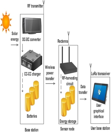
The sequence of the design follows the path of energy transfer from the solar panel to the batteries to the RF amplifier to the receiving antenna and to the energy harvesting circuit. A complete system visualization is shown in
Figure 2.
4.1. Power Base Station (FU1)
The reason for implementing a power base station is to use the harvested solar energy to charge lithium-ion batteries which in turn are used to power the RF transmitter. Firstly, the voltage from the solar panel needs to be stepped down to a desired voltage level. To achieve this, either a linear regular or a DC-DC converter can be utilized. In this work a DC-DC converter was selected because of its higher efficiency in stepping down voltage. Similarly, the CC-CV charging algorithm used for effectively charging the batteries can either be executed by a current limiting circuit cascaded with a voltage limiting circuit or by controlling the DC-DC converter with a microcontroller. Furthermore, a MOSFET instead of an IGBT was used as a switch for the DC-DC converter due to a MOSFET medium output impedance and fast switching speed. This is because an increase in switching frequency will result in a decrease output current and voltage ripple [
36,
37,
38].
4.2. Step-Down DC-DC Converter Design (FU1.2)
The purpose of the DC-DC converter is to step the voltage fed by the 50 W solar panel down to the voltage required to charge Li-ion batteries. The converter is controlled using a high frequency pulse width modulated (PWM) signal generated by a microcontroller. The duty ratio of the PWM signal determines the output voltage of the converter. The power base station requires two 2200 mAh Li-ion batteries to operate. It was decided to place the batteries in series. This decision was made to ensure that at any state of charge, the batteries combined voltage would be greater than 5 V. Additionally, the batteries being placed in series requires less current to flow through the step-down DC-DC converter than if they were placed in parallel. A higher output voltage requires a higher duty ratio which results in a slightly higher overall efficiency. A switching frequency of 50 kHz was determined through practical observation to provide acceptable output ripple and small enough losses. To fulfil the requirements of the CC-CV charging of the Li-ion batteries connected in series, the converter should have an output current of 1.1 A and an output voltage ranging from 5.6 V to 8.4 V (2.8 V to 4.2 V per cell). Ferrite toroidal inductors were selected due to low magnetic losses. The resistance of one inductor was measured as = 375 mΩ. In practical implementation of the converter, four inductors were placed in series yielding a total resistance of = 1.5 Ω. The inductance of each inductor was chosen to be 88 mH for a total inductance of = 352 mH. An electrolytic capacitor with a capacitance of = 3300 was chosen. From the PR6003-T diode datasheet, the forward voltage drop is given as = 1.2 V. Whereas, in the IRF3205 datasheet, the drain-to-source current is given as . In the CSRB20G10L00 datasheets, shunt resistor is given as = 10 mΩ. Due to the resistance of the inductors being significantly higher, the shunt resistance was taken to be negligibly small, thus = 0 mΩ. Two cases were considered in the theoretical analysis DC-DC converter to determine the minimum size of the storage components.
Case 1: when
and
The voltage across the inductor is taken by applying the Kirchhoff voltage law to the converter when the MOSFET is on:
To ensure that the converter operates in continuous conduction mode, the current ripple (
) should not exceed a maximum value of
with a switching frequency of
the minimum size of the inductor was calculated as:
With an output current ripple of
, to maintain a maximum output voltage ripple of
, the minimum size of the capacitor was calculated as:
The average input current
was calculated as:
The input power
) was calculated as:
The output power
) was calculated as:
The overall efficiency
was calculated as:
Case 2: when
and
, and by applying Equation (2)
. The voltage across the inductor is obtained using Equation (3) as
. Also, with the maximum current ripple of
and a switching frequency of
the minimum size of the inductor was obtained using Equation (4) as
. Furthermore, with the maximum current ripple of
, to maintain a maximum output ripple of
, the minimum size of the capacitor was obtained using Equations (5) and (6) as
. Whereas, the average input current
was obtained as
using Equation (7) the input power
) was obtained as
using Equation (8) and the output power
) using Equation (9) is obtained as
. Therefore, the overall efficiency
was calculated as:
4.3. Microcontroller Input Design
Due to the solar PV input to the DC-DC converter, and the CC-CV Li-ion battery charging output of the DC-DC converter, both the input and output of the converter are variable. As such there exists the need for a dynamic control of the converter according to its input and output. By extension, there is a need for circuitry that acts as input to the microcontroller. To monitor the voltage output, a simple voltage dividing network of resistors was used in conjunction with a non-inverting operational amplifier. The circuit that provides voltage information to the microcontroller was simulated using OrCAD and is shown in
Figure 3.
With an input voltage of
and a resistance
and
the output of the non-inverting amplifier was calculated as:
The calculated output voltage value is congruent with the simulated output voltage value. To monitor the current output, the voltage across a
shunt resistor was fed through a differential operational amplifier. However, due to the large voltage outputs from the difference amplifier when no current flows through the shunt resistor, the output of the difference amplifier was fed to a non-inverting amplifier with a supply voltage of
. This is to ensure that the voltage present on the ADC input pin of the microcontroller does not exceed
. The circuit that provides current information to the microcontroller is shown in
Figure 4.
The expected input to the differential amplifier is the voltage across the
shunt resistor. Assuming a current of
flows through the shunt resistor the voltage difference will be
. When the resistors are selected such that
and
the differential amplifier equation is simplified to:
With
and
we obtained
. The output of the non-inverting amplifier was obtained as:
The simulated output values of and are congruent with the calculated values.
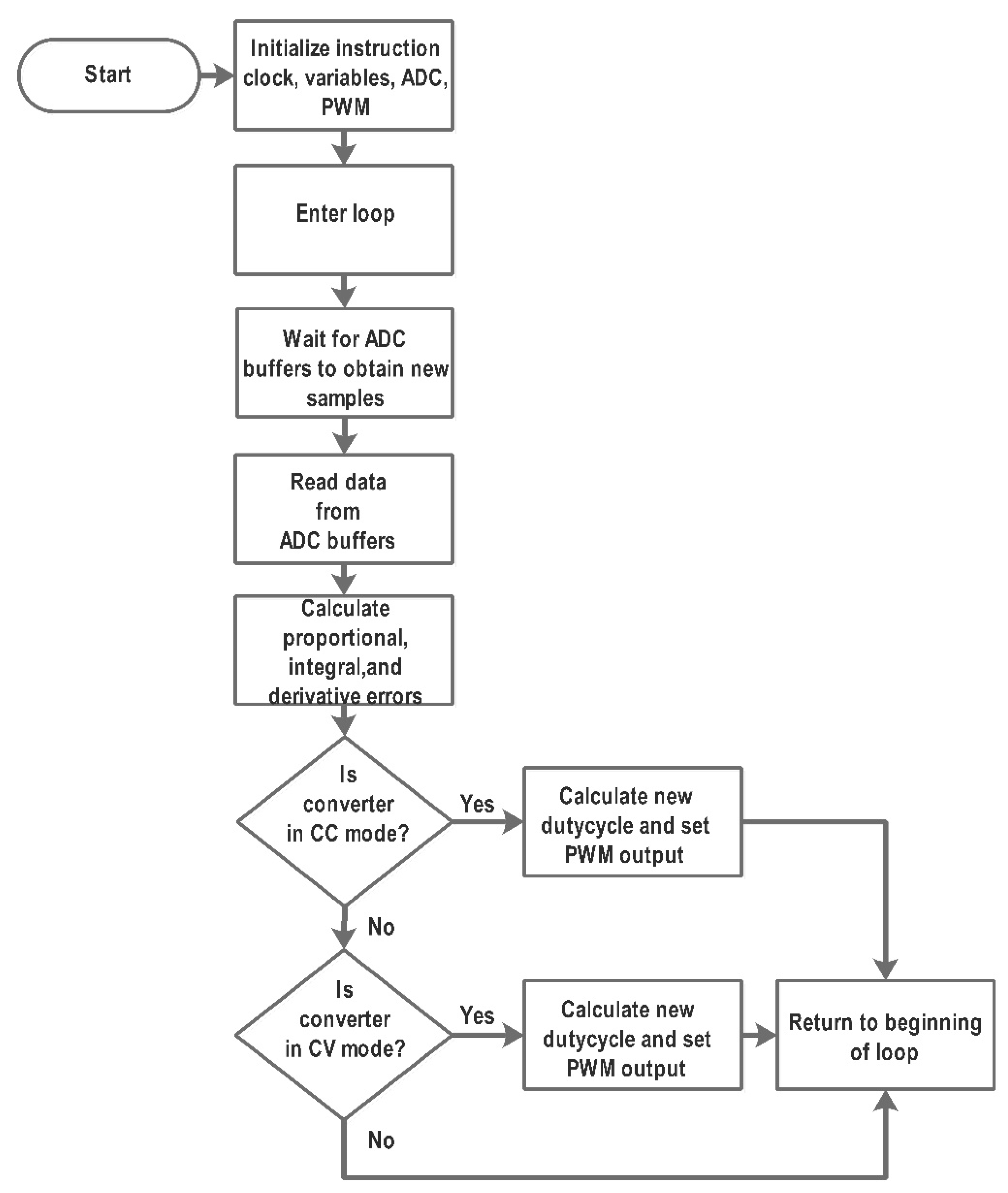
4.4. Microcontroller Firmware Design
The microcontroller chosen for the control of the DC-DC converter and implementation of the CC-CV charging of the Li-ion batteries was the PIC32MX220F032 (Microchip, Chandler, AZ, USA ). To meet the requirements of the CC-CV battery charging system, the microprocessor needs to meet a number of requirements. The resolution of the analogue to digital display (ADC) module affects how accurately the microprocessor reads the voltage and current outputs of the DC-DC converter. The resolution of the PWM module affects how accurately the microprocessor adjusts the duty ratio of the MOSFET in the DC-DC converter. The instruction clock frequency affects how rapidly the control system implemented on the microprocessor responds to differences between the desired set-point and the actual output. The requirements of the microprocessor are summarized in the
Table 2.
In
Figure 5, the program flow of the implementation of the microcontroller firmware is presented.
4.5. PID Controller Design
To ensure a stable output current and voltage of the step-down DC-DC converter, a proportional integral derivative (PID) control was applied to the converter. This is of importance when dealing with lithium-ion rechargeable batteries which can experience permanent damage if exposed to overvoltage or overcurrent conditions. Therefore, a continuous cycling test was performed to obtain the ultimate period (
) and the ultimate gain (
) of the system responsible for controlling the CC-CV charging of the Li-ion batteries. Based on the experiment performed, the ultimate gain associated with the undamped response of the system was recorded as
= 0.1525 µs whereas the ultimate period of the undamped response was measured as
= 520 µs. Subsequently, the obtained ultimate gain and ultimate period of the system were used to calculate the tuning parameter of the PID. In addition, the continuous cycling method used to obtain the ultimate gain and ultimate period is often used in conjunction with the Ziegler-Nichols tuning parameters. However, because the Ziegler-Nichols tuning parameters is undesirable for the CC-CV charging algorithm a less aggressive Tyreus-Luyben modified Ziegler-Nichols tuning rules were applied. The Ziegler-Nichols tuning parameters has a decay ratio which produces a response with overshoot and short settling time which often result in over-voltage or over-current. The Tyreus-Luyben tuning parameters are given in
Table 3.
Based on the experimentally obtained ultimate gain and ultimate period, the Tyreus-Luyben tuning parameters were calculated as follows: , and . Thereafter, the PID control is implemented through the PIC32MX220F032 microcontroller.
4.6. Antenna (FU2.2)
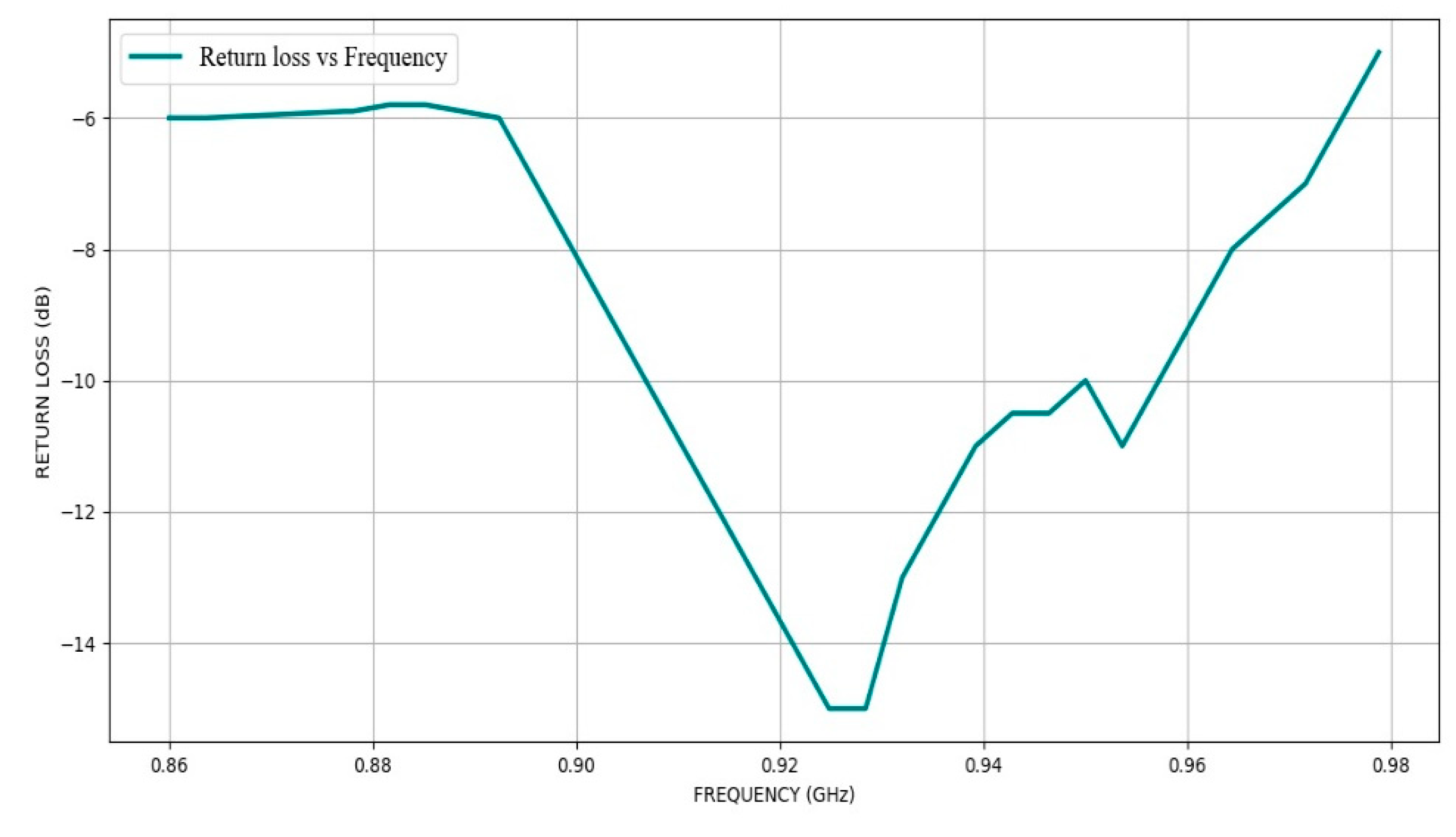
A stacked micro-strip patch antenna was selected to be used as the antenna type. The antenna was simulated using FEKO with various materials. After several iterations of design, a 0.7 mm thick copper conductor was selected and polystyrene was selected for the substrate. However, the stacked micro-strip patch antenna did not meet the requirements of the system. Therefore, the approach was adjusted and a Yagi antenna [
39], which consists of the stacking of
dipoles was designed. The antenna implementation flow diagram is shown in
Figure 6.
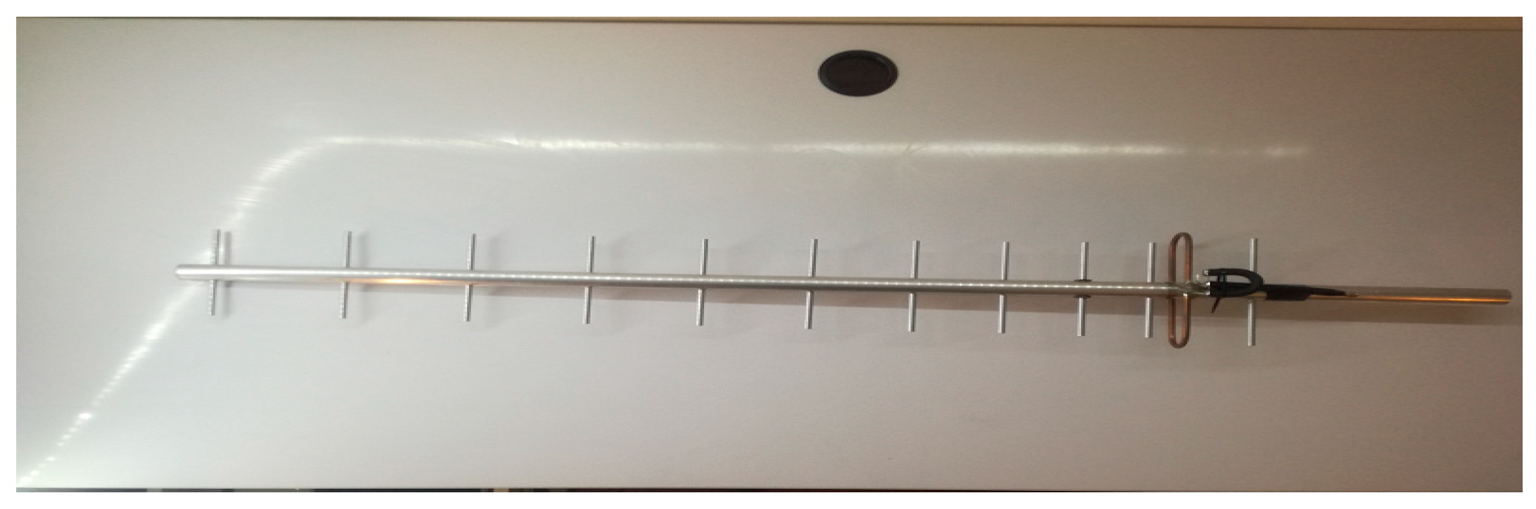
4.7. Yagi Antenna Design
The starting point for the Yagi antenna design was obtained from the National Bureau of Standards (NBS) paper [
40] with adjustment of the reflector spacing to 0.25 lambda which has been found to be a near optimum value [
41]. The thickness, length and spacing of the antenna elements affect the overall performance of the antenna. It was decided to set a fixed element thickness based on availability of materials. Using this element thickness, the element spacing and lengths were optimized. It was found that aluminum rods were available with an outer diameter of 6.35 mm and copper rods were available with an outer diameter of 6 mm. The active element (folded dipole) was to be constructed with copper rod, and the parasitic elements (reflector and directors) were to be constructed with aluminum rod. The Yagi antenna was simulated using the FEKO electromagnetic simulation software. The Yagi antenna was simulated with perfect electrical conductors (PEC) as the resistance present on aluminum and copper rods is sufficiently small to be considered zero. The antenna was simulated without the conducting aluminum tube boom. This was found to be computationally expensive and impractical for optimization searches. As such, the antenna was optimized using free-standing elements. A boom correction factor obtained from experimental data was applied to the elements before construction of the antenna. An optimization search was set up to optimize the realized gain and return loss at 920 MHz. It was found that optimizing for total gain as opposed to realized gain would compromise the return loss goal. The length and spacing of the director, reflector and driven elements were entered as parameters in the optimization search. The final iteration of the Yagi antenna optimization had a simulated gain of 15.0108 dBi and a return loss of −21.7774 dB at 920 MHz. The Yagi antenna dimensions are summarized in
Table 4. The driven element length is given from tip to tip which is more significant than the total length of the folded rod.
A table saw was used to cut the aluminum tube and rod into the desired sizes. Pieces of wood were cut and measured to obtain the desired length before cutting the aluminum. The director and reflector elements were filed and measured with a Vernier gauge to obtain an accuracy of within 0.2 mm. A drill press was used to drill holes into the Aluminum tube and the director and reflector elements were tapped into their respective holes. The copper rod was cut using a hack saw and was bent using a wooden jig. The folded dipole was attached to the aluminum tube using metal corner pieces, hose clamps, and a nut and bolt.
Figure 7 shows the designed Yagi antenna.
4.8. Energy Harvesting Circuit (FU2.2)
The intended achieved gain for the antenna was 6 dBi. Assuming that this was achieved, an input power of −11.44 dBm would be available when the sensor node is placed 15 m from the RF source. This input power does not require a highly sensitive RF-to-DC converter. As such, the diode-based Dickson RF-DC converter (city, state abbrev if USA, country) was chosen. The Dickson RF-DC rectifier was simulated using the HSMS-2860 Schottky diode model and ideal capacitors. When tested, the Dickson RF-DC converter did not have a high enough efficiency. The approach was adjusted, and a transistor based fully cross-coupled rectifier circuit was designed. The fully cross-coupled rectifier circuit was simulated using HFA3096 transistors (Renesas, city, state abbrev if USA, country_ and ideal capacitors. Simulations of the energy harvesting circuit were done in LTSpice XVII, a high performance SPICE simulation software. LTSpice XVII has circuit capture and waveform viewer functionality. The RF-DC flow diagram is shown in
Figure 8.
4.9. Energy Harvesting Circuit Design (FU2.2)
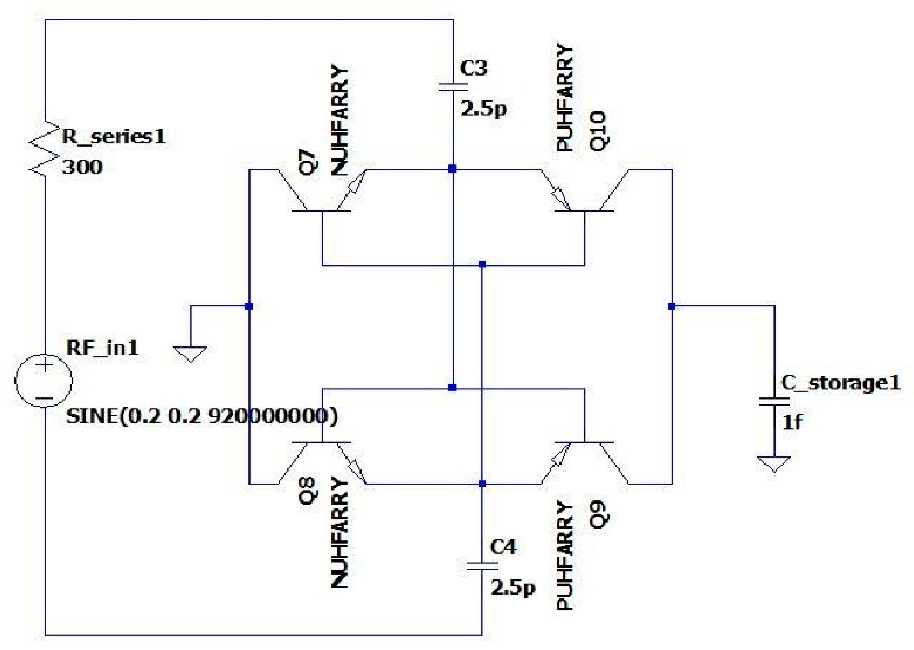
4.9.1. Fully Cross-Coupled RF-DC Converter
A transistor-based fully cross-coupled radio frequency-direct current (RF-DC) converter circuit was simulated using LTSpice XVII. Additionally, a Renesas HFA3096BZ ultra high frequency transistor arrays were selected for the fully cross coupled RF-DC converter. Furthermore, the fully cross-coupled RF-DC converter was simulated with one and two stages. However, it was found that the 2-stage circuit was approximately half as efficient and did not provide a significant increase in voltage across the storage capacitor. Therefore, a single stage fully cross-coupled RF-DC converter circuit with Renesas HFA3096BZ transistor is implemented. The implemented circuit is presented in
Figure 9.
4.9.2. Step-Up DC-DC Converter
The boost converter was designed to be controlled by a microcontroller. In order to provide the microcontroller with the necessary voltage, a 551 timer is turned on through the use of a momentary switch. The 551 timer drives the boost converter MOSFET while the momentary switch is on. The boost converter outputs a voltage which is regulated to 3.3 V and fed to the microcontroller. Once the momentary switch is released (off), the MOSFET is driven by the microcontroller. The purpose of the DC-DC converter is to boost the voltage stored on the supercapacitor to a voltage usable by the sensor node (≥3.3 V). The step-up converter was designed to be connected to a
low dropout voltage regulator. The converter is controlled using a high frequency PWM signal generated by a microcontroller. The duty ratio of the PWM signal determines the output voltage of the converter. The frequency of the PWM signal has an inverse relationship on the output current and voltage ripple; An increase in the switching frequency results in a decrease in ripple. The frequency is directly proportional to switching losses of the MOSFET, and hysteresis losses of the inductor. The voltage regulator was assumed to have a
dropout while delivering the required current. The MOSFET is assumed to have a drain-source voltage drop of
. The diode is assumed to have a forward voltage drop of
The resistance of the inductor is assumed to be
. The boost converter was simulated with a switching frequency of
The step-up DC-DC converter was simulated using LTSpiceXVII. The simulation was used to evaluate 16 different MOSFET options, and nine different diode options. Once the most suitable MOSFET and diode options were chosen, the circuit was simulated using ideal voltage controlled switches to charge a capacitor representing a supercapacitor, and to subsequently provide the converter with an input voltage from the supercapacitor. The MOSFET was controlled using a
PWM voltage source. A constant power load was powered by the boost converter through a
voltage regulator. The power consumption of the load was calculated using the expected power draw of the sensor node as well as the efficiency of the voltage regulator which lies between the step-up converter and the MDOT module. The duty cycle of the PWM voltage source, inductance and capacitance were adjusted to optimize the time that the load could be supplied with a voltage greater than
. Using the selected components, the step-up converter was simulated to determine the optimum size of the capacitor. The boost converter was simulated using the maximum effective constant duty cycle to determine the minimum size supercapacitor required to provide
of power for a duration of
. It was found that the optimum output capacitance was
and that the minimum capacitance of the supercapacitor was
.
Figure 10 shows the sensor node circuit containing the fully cross-coupled RF-DC converter, the step-up DC-DC converter, the MDOT LoRa module [
42,
43], and the Microchip MCP9700 temperature sensor.
4.10. Design of the Multitech LoRa Communication
To implement LoRa communication, two LoRa MDOT-868 modules (Multitech, Mounds View, MN 55112, USA) were used. The Multitech MTUDK2-ST-MDOT development board was used to program the LoRa modules. The arm mbed development platform’s compiler was used to alter and compile code. The MDOTs work in peer-to-peer mode using example code from Multitech. In peer-to-peer mode, the MDOTs are constantly in receive mode, unless transmitting data.
4.11. Sensor Node
Apart from the transmission of data to the user, the main objective in the design of the sensor node MDOT firmware was to transmit data in the shortest timeframe possible and thus decrease the overall energy requirement of the sensor node. The join delay was set to
The default join delay is
The transmit power was set to the lowest level of
. The data rate was set to the fastest available data rate for use in the Europe region. Although the higher data rate consumes more power, the MDOT operates for a shorter duration which improves overall energy consumption. Two possible temperature sensor ICs were investigated.
Table 5 shows a comparison of the features of the Dallas 18B20 and Microchip MCP9700 temperature sensors.
The Microchip MCP9700 was selected for use in the sensor node due to its low active current and lack of conversion time. The sensor node MTDOT obtains a temperature reading from the Microchip MCP9700 temperature sensor via the mbed AnalogIn Driver Application Programming Interface (API). The temperature float variable is split into two integers, one representing the whole number and the other representing the fraction. The two integers are concatenated into one longer integer and sent via LoRa to the user base station MDOT. For debugging purposes during the development of the MDOT firmware, the temperature value read from the temperature sensor was outputted to the serial port.


