Figure 1.
Impedance source inverter basic block diagram.
Figure 1.
Impedance source inverter basic block diagram.
Figure 2.
Impedance source inverter operation: (a) impedance source circuit, shoot through (ST) state, an active state, (b) inductor current and capacitor voltage idealized condition waveforms.
Figure 2.
Impedance source inverter operation: (a) impedance source circuit, shoot through (ST) state, an active state, (b) inductor current and capacitor voltage idealized condition waveforms.
Figure 3.
Boost-mode characteristics of Z-source inverter; (a) DC-link voltage versus input voltage, (b) inductance versus input voltage, and (c) input voltage response versus change in capacitances.
Figure 3.
Boost-mode characteristics of Z-source inverter; (a) DC-link voltage versus input voltage, (b) inductance versus input voltage, and (c) input voltage response versus change in capacitances.
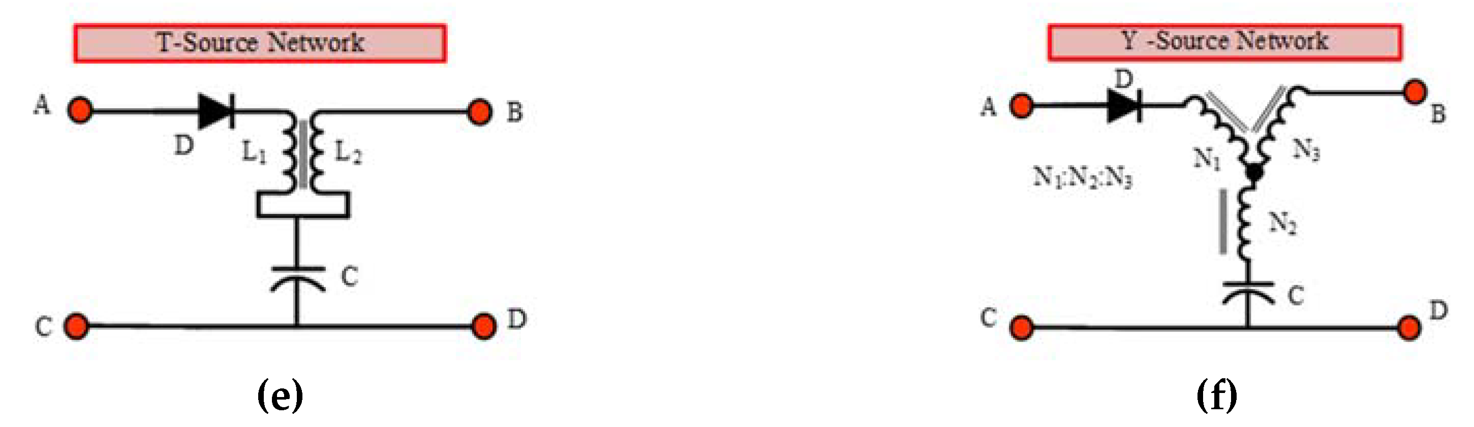
Figure 4.
Different Z-source topologies; (a) Z-source network, (b) Quasi-source network, (c) Modified Quasi-source network, (d) Trans Z-source network, (e) T-source network, (f) Y-source network.
Figure 4.
Different Z-source topologies; (a) Z-source network, (b) Quasi-source network, (c) Modified Quasi-source network, (d) Trans Z-source network, (e) T-source network, (f) Y-source network.
Figure 5.
Proposed modified Q-impedance converter fed coupled inductor multilevel inverter (MLI).
Figure 5.
Proposed modified Q-impedance converter fed coupled inductor multilevel inverter (MLI).
Figure 6.
Proposed modified Q-impedance network.
Figure 6.
Proposed modified Q-impedance network.
Figure 7.
States of proposed Q- impedance network topology; (a) State-1: active state, (b) State 2: shoot-through states, (c) State-3: open-zero states.
Figure 7.
States of proposed Q- impedance network topology; (a) State-1: active state, (b) State 2: shoot-through states, (c) State-3: open-zero states.
Figure 8.
(a) Converter operation in different modes, Vboost / input voltage (VPV) for duty cycle DA, (b) energy storage capability and voltage stress radar graph of conventional QZ and proposed QZ.
Figure 8.
(a) Converter operation in different modes, Vboost / input voltage (VPV) for duty cycle DA, (b) energy storage capability and voltage stress radar graph of conventional QZ and proposed QZ.
Figure 9.
Coupled inductor MLI.
Figure 9.
Coupled inductor MLI.
Figure 10.
During mode 1 the inverter switches S1, S4, and S6 are turned ON.
Figure 10.
During mode 1 the inverter switches S1, S4, and S6 are turned ON.
Figure 11.
During Mode-2, the inverter switches S1, S4, and S5 are turned ON.
Figure 11.
During Mode-2, the inverter switches S1, S4, and S5 are turned ON.
Figure 12.
During mode 3 the inverter switches S1, S3, and S6 are turned ON.
Figure 12.
During mode 3 the inverter switches S1, S3, and S6 are turned ON.
Figure 13.
During Mode-4 the inverter switches S1, S3, and S5 are turned ON.
Figure 13.
During Mode-4 the inverter switches S1, S3, and S5 are turned ON.
Figure 14.
During mode 5 the inverter switches S2, S4, and S6 are turned ON.
Figure 14.
During mode 5 the inverter switches S2, S4, and S6 are turned ON.
Figure 15.
During mode-6 the inverter switches S2, S4, and S5 are turned ON.
Figure 15.
During mode-6 the inverter switches S2, S4, and S5 are turned ON.
Figure 16.
During Mode-7 the inverter switches S2, S3, and S6 are turned ON.
Figure 16.
During Mode-7 the inverter switches S2, S3, and S6 are turned ON.
Figure 17.
During Mode-8 the inverter switches S2, S3, and S5 are turned ON.
Figure 17.
During Mode-8 the inverter switches S2, S3, and S5 are turned ON.
Figure 18.
Output voltage structure for proposed MLI.
Figure 18.
Output voltage structure for proposed MLI.
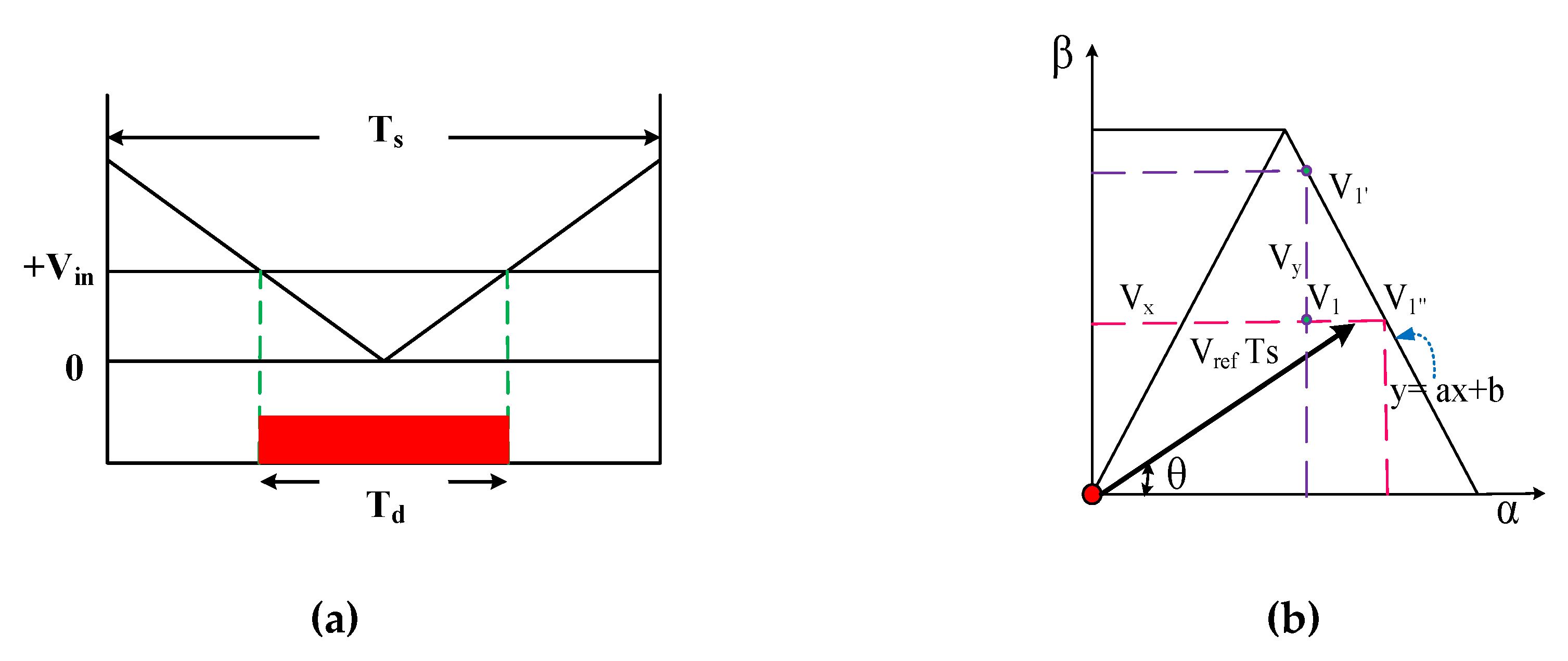
Figure 19.
(a) Dwell time switching states synthesis, (b) proposed control strategy Vref slope.
Figure 19.
(a) Dwell time switching states synthesis, (b) proposed control strategy Vref slope.
Figure 20.
Space vector diagram and switching table.
Figure 20.
Space vector diagram and switching table.
Figure 21.
Space vector PWM algorithm and switching table.
Figure 21.
Space vector PWM algorithm and switching table.
Figure 22.
Proposed impedance source Space vector PWM and switching table.
Figure 22.
Proposed impedance source Space vector PWM and switching table.
Figure 23.
Simulation diagram of the proposed photovoltaic (PV) powered modified Q-impedance converter fed coupled inductor MLI.
Figure 23.
Simulation diagram of the proposed photovoltaic (PV) powered modified Q-impedance converter fed coupled inductor MLI.
Figure 24.
Modified Q- impedance converter fed coupled inductor MLI.
Figure 24.
Modified Q- impedance converter fed coupled inductor MLI.
Figure 25.
ST state representations of S1 and S2.
Figure 25.
ST state representations of S1 and S2.
Figure 26.
Voltage waveform of impedance network capacitors at TST = 25%; (a) VC1, (b) VC2.
Figure 26.
Voltage waveform of impedance network capacitors at TST = 25%; (a) VC1, (b) VC2.
Figure 27.
Current waveform of impedance network inductor at TST = 25%; (a) L1, (b) L2.
Figure 27.
Current waveform of impedance network inductor at TST = 25%; (a) L1, (b) L2.
Figure 28.
Inverter DC-link voltage at TST = 25%.
Figure 28.
Inverter DC-link voltage at TST = 25%.
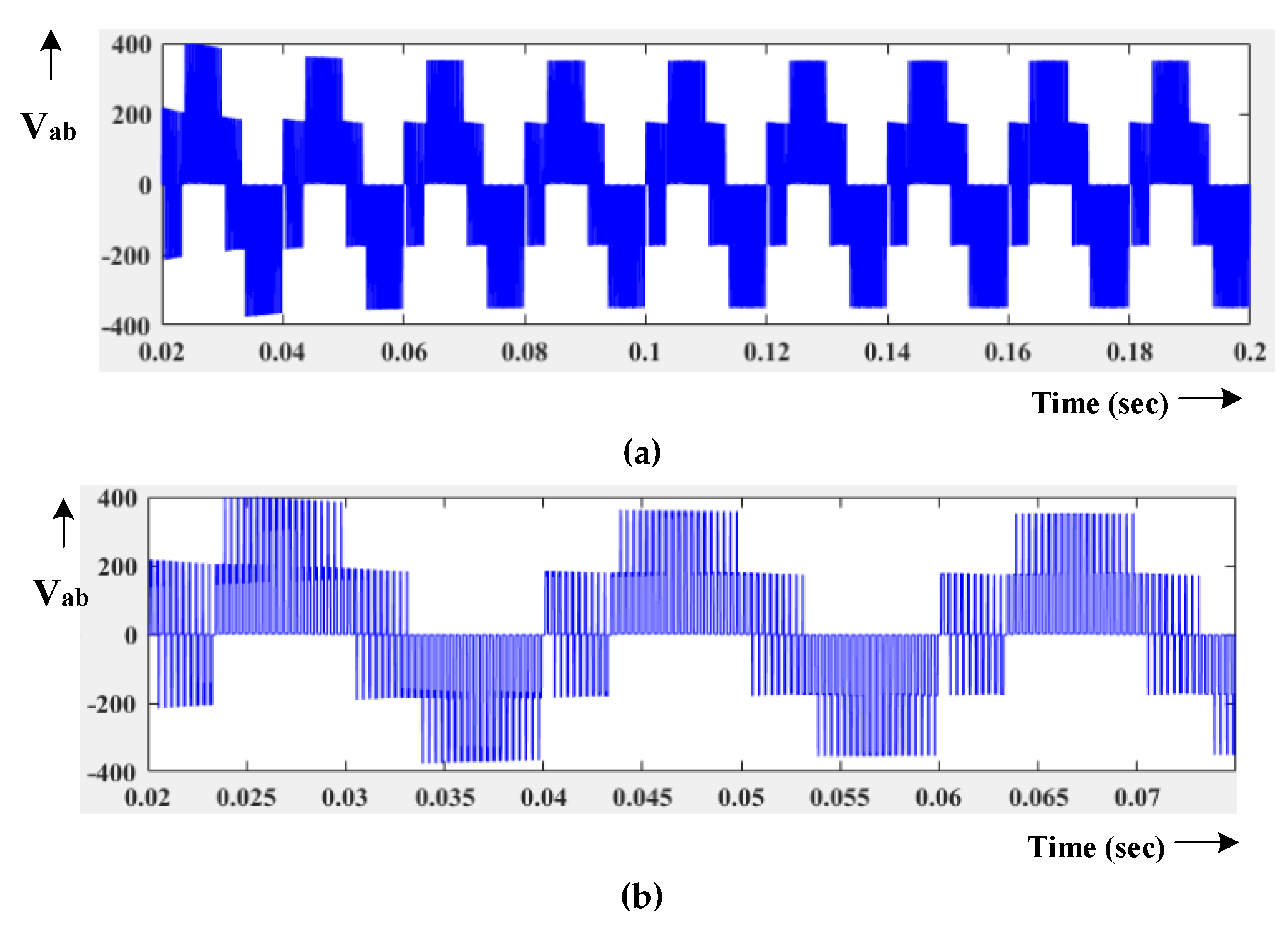
Figure 29.
(a) Inverter output voltage at TST = 25% without filter, (b) zoomed view of the inverter output voltage at TST = 25% without a filter.
Figure 29.
(a) Inverter output voltage at TST = 25% without filter, (b) zoomed view of the inverter output voltage at TST = 25% without a filter.
Figure 30.
THD profile of inverter output voltage when TST = 25% without a filter.
Figure 30.
THD profile of inverter output voltage when TST = 25% without a filter.
Figure 31.
Inverter output current at TST = 25% with filter.
Figure 31.
Inverter output current at TST = 25% with filter.
Figure 32.
THD profile of inverter output voltage at TST = 25% with filter.
Figure 32.
THD profile of inverter output voltage at TST = 25% with filter.
Figure 33.
(a) Inverter output current at TST = 25%, (b) THD profile of inverter output current at TST = 25%.
Figure 33.
(a) Inverter output current at TST = 25%, (b) THD profile of inverter output current at TST = 25%.
Figure 34.
Inverter DC-link voltage at TST = 20%.
Figure 34.
Inverter DC-link voltage at TST = 20%.
Figure 35.
Voltage waveform of impedance network capacitors at TST = 20%; (a) VC1, (b) VC2.
Figure 35.
Voltage waveform of impedance network capacitors at TST = 20%; (a) VC1, (b) VC2.
Figure 36.
(a) Inverter output voltage at TST = 25% without filter, (b) zoomed view of inverter output voltage at TST = 25% without filter.
Figure 36.
(a) Inverter output voltage at TST = 25% without filter, (b) zoomed view of inverter output voltage at TST = 25% without filter.
Figure 37.
THD profile of inverter output voltage at TST = 25% without a filter.
Figure 37.
THD profile of inverter output voltage at TST = 25% without a filter.
Figure 38.
(a) Inverter output voltage at TST = 30% without filter, (b) zoomed view of the inverter output voltage at TST = 30% without a filter.
Figure 38.
(a) Inverter output voltage at TST = 30% without filter, (b) zoomed view of the inverter output voltage at TST = 30% without a filter.
Figure 39.
THD profile of inverter output voltage at TST = 30%.
Figure 39.
THD profile of inverter output voltage at TST = 30%.
Figure 40.
Experimental setup; (a) overall laboratory-scale 500 W PV powered modified Q-impedance fed coupled inductor MLI, (b) modified Q-impedance fed coupled inductor MLI.
Figure 40.
Experimental setup; (a) overall laboratory-scale 500 W PV powered modified Q-impedance fed coupled inductor MLI, (b) modified Q-impedance fed coupled inductor MLI.
Figure 41.
PWM pulse generation (S1 and S2).
Figure 41.
PWM pulse generation (S1 and S2).
Figure 42.
Experimental result; (a) boost inductor current (iL1 and iL2), (b) voltage waveform of impedance network capacitors C1 and C2.
Figure 42.
Experimental result; (a) boost inductor current (iL1 and iL2), (b) voltage waveform of impedance network capacitors C1 and C2.
Figure 43.
Experimental result; (a) inverter five-level output voltage, (b) quasi Z-source inverter input current waveform.
Figure 43.
Experimental result; (a) inverter five-level output voltage, (b) quasi Z-source inverter input current waveform.
Figure 44.
Experimental voltage THD spectrum without a filter.
Figure 44.
Experimental voltage THD spectrum without a filter.
Figure 45.
Experimental result; (a) inverter output voltage with filter, (b) inverter output current waveform with filter.
Figure 45.
Experimental result; (a) inverter output voltage with filter, (b) inverter output current waveform with filter.
Figure 46.
Experimental result; (a) voltage THD spectrum with filter, (b) current THD spectrum with filter.
Figure 46.
Experimental result; (a) voltage THD spectrum with filter, (b) current THD spectrum with filter.
Figure 47.
Experimental result; (a) quasi Z-source coupled MLI output voltage and input current at DST = 25%, (b) quasi Z-source coupled MLI output voltage and input current at DST = 30%.
Figure 47.
Experimental result; (a) quasi Z-source coupled MLI output voltage and input current at DST = 25%, (b) quasi Z-source coupled MLI output voltage and input current at DST = 30%.
Figure 48.
Passive components rating, cost, boosting, and THD comparisons; (
a) Reference [
39], (
b), Reference [
41], (
c) Reference [
39], (
d) proposed QZ Inverter.
Figure 48.
Passive components rating, cost, boosting, and THD comparisons; (
a) Reference [
39], (
b), Reference [
41], (
c) Reference [
39], (
d) proposed QZ Inverter.
Table 1.
Switching table for the proposed topology.
Table 1.
Switching table for the proposed topology.
| Mode | Conducting Switches | Output |
|---|
| 1 | S1, S4, S6 | |
| 2 | S1, S4, S5 | |
| 3 | S1, S3, S6 | |
| 4 | S1, S3, S5 | |
| 5 | S2, S4, S6 | |
| 6 | S2, S4, S5 | |
| 7 | S2, S3, S6 | |
| 8 | S2, S3, S5 | |
Table 2.
Simulation Parameters.
Table 2.
Simulation Parameters.
| Input PV Voltage, VPV | 100 V–120 V |
|---|
| Impedance Network Inductor Ls = L2 = L3 | 2 mH |
| Impedance network inductor capacitors C1 = C2 | 200 µF |
| Switching frequency, fs | 10 KHz |
| Inverter coupled inductor LM1 = LM2 | 5 mH |
| Mutual inductance | 2.4 mH |
| Load resistance and inductance | 10Ω, 5 mH |
| LC filter: inductance and capacitor | 2.5 mH,50 µF |
Table 3.
Detailed simulation results for different duty ratio without an LC filter at ma = 0.86 and 0.6.
Table 3.
Detailed simulation results for different duty ratio without an LC filter at ma = 0.86 and 0.6.
| DST | Vin | Vo = VDC-link | Vab for ma = 0.86 | % THD Vab for ma = 0.86 | Vab for ma = 0.60 | % THD Vab for ma = 0.60 |
|---|
| 0 | 120 | 120 | 86.4 V | 13.6% | 59.3 V | 12.6% |
| 10% | 120 | 177 | 125.6 V | 13.9% | 88.5 V | 13.8% |
| 15% | 120 | 210 | 149.2 V | 14.06% | 99.1 V | 13.8% |
| 20% | 120 | 280 | 197.4 V | 14.11% | 135.3 V | 13.54% |
| 25% | 120 | 349 | 247.3 V | 14.15% | 166.7 V | 14.06% |
| 30% | 120 | 410 | 291.7 V | 19.55% | 201.6 V | 17.32% |
Table 4.
Detailed simulation results for different duty ratio with an LC filter at ma = 0.86 and 0.6.
Table 4.
Detailed simulation results for different duty ratio with an LC filter at ma = 0.86 and 0.6.
| DST | Vin | Vo = VDC-link | Vab for ma =0.86 | % THD Vab for ma =0.86 | Vab for ma =0.60 | % THD Vab for ma =0.60 |
|---|
| 0 | 120 | 120 | 85.1 V | 2.69% | 57.2 V | 2.61% |
| 10% | 120 | 177 | 123.9 V | 2.71% | 86.9 V | 2.68% |
| 15% | 120 | 210 | 147.1 V | 2.72% | 97.4 V | 2.72% |
| 20% | 120 | 280 | 195.9 V | 2.77% | 133.9 V | 2.74% |
| 25% | 120 | 349 | 241.2 V | 2.81% | 164.9 V | 2.79% |
| 30% | 120 | 410 | 291.7 V | 3.83% | 200.1 V | 3.68% |
Table 5.
Switching loss, inverter efficiency, and THD of the proposed inverter for ma = 0.86 and fs = 10 kHz concerning DST from 10% to 30%.
Table 5.
Switching loss, inverter efficiency, and THD of the proposed inverter for ma = 0.86 and fs = 10 kHz concerning DST from 10% to 30%.
| DST | Switching Loss in Watts | Conduction Loss in Watts | Inverter Efficiency in % | THD in %(without Filter) | THD in %(with Filter) |
|---|
| 10% | 6.4 | 15.2 | 95.68% | 13.9% | 2.72% |
| 20% | 9.4 | 16.6 | 94.8% | 14.11% | 2.77% |
| 30% | 15.2 | 17.3 | 93.5% | 19.55% | 3.83% |
Table 6.
Switching loss, inverter efficiency, and THD of the proposed inverter for ma = 0.86 and fs = 10 kHz concerning DST from 10% to 30%.
Table 6.
Switching loss, inverter efficiency, and THD of the proposed inverter for ma = 0.86 and fs = 10 kHz concerning DST from 10% to 30%.
| Topology Proposed in | Number of Passive Elements Used | Number of Switches Used | A Coupled Inductor or Transformer Type | Maximum Achievable Voltage Gain in % |
|---|
| L | C |
|---|
| [39] | 2 | 2 | 6 | Coupled inductor | ≤ 2 times |
| [6] | 2 | Intergraded winding | 8 | NA | ≤ 2 times |
| [45] | 4 | 2 | 2 only for converter | Coupled inductor | ≥ 2 times |
| [46] | 4 | 4 | 8 | NA | |
| [47] | 4 | 4 | 8 | NA | ≤ 2 times |
| [48] | 2 | 2 | 10 | NA | ≤ 2 times |
| Proposed QZ Inverter | 3 | 2 | 6 | Coupled inductor | ≥ 2 times |

 ,
, 


