1. Introduction
Microwave wireless power transfer (MRWPT) is being actively studied as a technology for wireless charging in various environments, such as artificial satellites, medical devices, and smart offices. MRWPT is a method of radiating generated microwave power to phased array antennas and supplying power through an electromagnetic field. MRWPT can transmit a longer distance than magnetic resonant WPT, but the power transfer efficiency (PTE) decreases as the transmitter (TX) and receiver (RX) distance increases. The performance of the MRWPT is determined not only by the PTE but also by the power amplifier (PA), phased array antenna (PAA), beamforming algorithm and receiver performance [
1].
The RX for MRWPT is used not only for WPT but also for energy harvesting. It consists of an array receiving antenna, the impedance matching unit, the rectifier, and a load. The part that determines the performance of the receiver is the rectifier. There are various rectifier design methods [
1,
2,
3,
4,
5,
6]. A half-wave rectifier circuit [
1,
2] can convert the input signal in the positive or negative region to DC by arranging Schottky diodes in series or shunts. A series of diode rectifiers was proposed, and a dual-band rectenna at 2.4 and 5.8 GHz was designed [
1].
The power conversion efficiency (PCE) of the rectifier is 63% at 2.4 GHz and 54.8% at 5.8 GHz at an input power of 10 mW. A shunt diode rectifier using load-pull [
2] has PCE of 63% at an input power of 10 dBm. Although the shunt diode rectifier requires low design difficulty with simple structure, it has low rectification efficiency and a very high impedance of the load. A full-wave rectifier circuit, which converts the entire input signal to DC using two or four Schottky diodes, with harmonic termination of 5.8 GHz signal has PCE of 65.3% at 15 dBm [
3]. It has higher rectification efficiency than a half-wave rectifier circuit [
1].
However, its structure is complicated. A Class C single Schottky diode rectifier and Class F
GaN transistor rectifier based on the power amplifier theory was also proposed [
4]. A Class C rectifier operating at a 2.45 GHz band uses a shunt diode shorted to the second and third harmonics. It has a PCE of 72% at an input power of 7 dBm [
4]. A Class F rectifier using even order harmonic control with shorted stubs and odd order harmonic control with open stubs has been proposed [
5]. When operating at 5.81 GHz, it has a PCE of 69.2% using series diode and harmonic cancellation at an input power of 8.2 dBm [
5]. A Class F rectifier using Dickson charge pump in 5.2 GHz band has a PCE of 64% at an input power of 23 dBm [
6].
As mentioned above, there have been studies on the design of rectifiers using various topologies. However, Refs. [
5,
6] targeted systems that convert relatively low RF power into DC, such as energy harvesting and Internet of Things (IoT) sensor driving. However, the power density delivered to the receiver varies depending on the surrounding environment and location. In the wireless power transfer environment, the received power density changes due to the distance of the transmitting/receiving antenna, beamforming performance, etc., in particular.
Existing topologies [
5,
6] are challenging to apply to a wireless power transfer system to which a high power density is used due to the performance limitations of diodes. Therefore, it is necessary to design a rectifier with high PCE according to various input powers. This paper proposes a rectifier design that shows PCE when high power density is applied in various wireless power transfer environments.
Ref. [
7] proposed a rectenna design that exhibits more than 50% PCE in a wide range of input power (−10∼25 dBm) in a wireless power transfer system. Ref. [
7] designed an impedance matching unit according to low power density and high power density and showed a maximum PCE performance of 70.2% at an input power of 17 dBm. Ref. [
8] proposed array rectifiers with an adaptive power distribution network (APDN). APDN consists of a rectifier cell for high frequency and high power and a rectifier cell for low frequency and low power intensity.
Ref. [
9] designed a rectenna showing high PCE (86%) performance at high input power (27 dBm) in a scenario where multi-tone (1.7 GHz and 2.4 GHz) is applied to the receiver. Ref. [
10] proposed a rectifier designed to operate in various frequency ranges by using harmonic termination when a two-tone or four-tone signal is applied to the receiver.
Ref. [
11] proposed a power recycling network (PRN) during a study to receive a wide input power range in a wireless power transmission environment and showed more than 50% PCE performance in the input power range of 10.5∼31.8 dBm. The PRN consists of two rectifier cells, and unlike [
8], an impedance matching unit was designed so that the reflected power can be applied to other rectifier cells.
Ref. [
12] proposed a structure of two rectifier cells like [
8,
11], and, to compensate for the reflected power, a hybrid coupler and a phase shift unit were implemented. The rectifier circuit proposed in [
12] showed more than 50% of PCE performance even when the size range of the load (8 to 97 k
) was wide. The diodes used in studies covering the low input power range to the wide input power range were mainly Schottky diodes. Ref. [
13] proposed a wire-bonded GaN diode rectifier to show high performance at high input power.
As above, existing studies have proposed a rectifier operating at relatively low power and high load impedance [
1,
2,
3,
4,
5,
6], or a receiver operating over a wide input power range in a changing wireless power transfer environment [
7,
8,
9,
10,
11,
12]. Alternatively, a rectifier using a GaN device for high input power has been proposed. GaN diodes exhibit higher breakdown voltage characteristics than Schottky diodes made of silicon, and thus they are suitable for high input power devices. The design difficulty of GaN diodes in the C-Band (4∼8 GHz) or higher band is very difficult, and the manufacturing cost is high.
However, to sufficiently supply power to devices, such as sensors and smartphones through PAA beamforming, it is necessary to design and mathematically analyze a rectifier with high PCE performance at high input power. Since a diode or transistor, which is a core element of a rectifier, is a nonlinear element, it is essential to design it through a nonlinear analysis and a behavioral model [
14,
15]. In addition, a diode must be selected according to the input power level, and a rectifier was designed based on the electrical characteristics of the adopted diode.
In this paper, we propose a method to derive the output voltage, current, and power loss of the rectifier to be designed using a nonlinear mathematical approach based on the electrical characteristics of the diode. Therefore, the proposed method was analyzed using the voltage and current waveforms of diodes, and a harmonic termination filter was designed to improve switching efficiency. Finally, an N-stage harmonic terminated voltage multiplier (N-stage HTVM) was designed. The proposed N-stage HTVM was analyzed with mathematical analysis of the diode waveform and power loss of the diode.
This paper is prepared with the following structure. First, the mathematical analysis of the proposed rectifier is shown in
Section 2.
Section 3 describes the design process of the harmonic termination filter. The performance of the N-stage HTVM is validated by simulation and measurement in
Section 4, and our conclusions are made in
Section 5.
3. Design Method of Harmonic Termination Filter
The harmonic termination (HT) filter can be designed through the transmission line theory. A HT filter is mainly designed to pass and block with an input impedance determined by the electrical length of the open-ended stub and short stub. There are various other HT filter design methods. In this paper, only open-ended stubs are used and designed as shown in
Figure 4. The filter is designed using only open stubs because it is easy to design. In addition, characteristics do not change dramatically even when the deformed form is the same as the bent form. Thus, it is suitable for miniaturization and tuning.
The third harmonic term appears to be short in the admittance characteristic seen from the input terminal of the open-ended stub having an electrical length of
. However, its impedance characteristic, which is the reciprocal of it, appears to be open. Therefore, the impedance characteristics of harmonic components seen from the input
can be expressed as follows:
where
is the characteristic impedance of
electrical length open-ended stub, and
is the fundamental angular frequency. As for the input admittance characteristics of an open-ended stub having an electrical length of
, the second harmonic term appears to be open, and the third harmonic term appears to be short. However, since the impedance characteristic seen from the input terminal has an inverse relationship, the second harmonic term seems to be short, and the third harmonic term appears to be open, which can be expressed as the following equation:
where
is the characteristic impedance of
electrical length open-ended stub. The HT filter was designed with impedance characteristics obtained from Equations (21) and (22). The sum of electrical lengths of transmission lines between each stub is
. Furthermore, if double open-ended stubs are configured, the characteristic impedance is reduced. Thus, the bandwidth increases, rather than composing an HT filter with one open-ended stub, as shown in
Figure 4.
Figure 5 shows input impedance and E-field through EM simulation of the designed filter.
When the center frequency of the HT filter designed in
Figure 5 is 5.8 GHz, odd harmonic terms (5.8 and 17.4 GHz) seems to be open, while even harmonic term (11.6 GHz) seems to be short. EM simulation confirmed that the desired frequency characteristics were obtained from the E-field distribution.
4. Simulation and Measurement
The performance of N-stage HTVM was determined through model verification and circuit simulation based on measurement results.
Table 1 shows the parameters used for model verification and circuit simulation.
Figure 6 shows diode voltage and current waveforms in the time domain, and
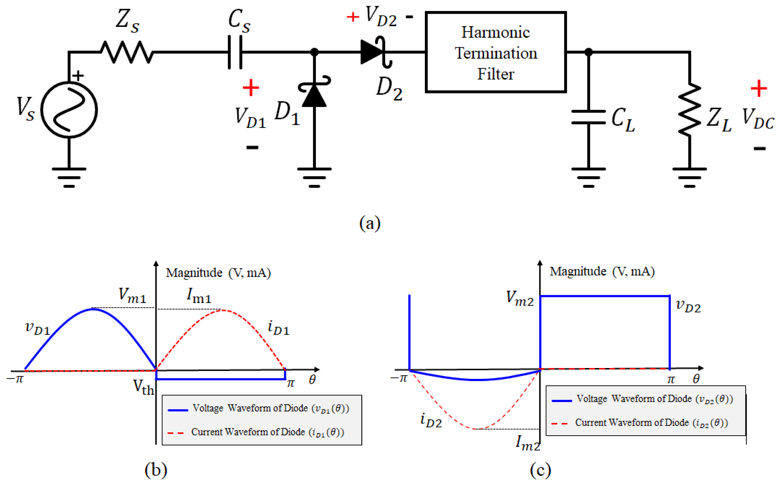
Figure 7 shows harmonics in the frequency domain when the number of stages is 1–3. One of the reasons for the difference between
Figure 2,
Figure 3 and
Figure 6 is that
and
have different sizes. As
and
are smaller, the voltage waveform of the diode appears ideally.
Figure 6 shows a simulation using the actual diode parameters shown in
Table 1.
As the number of stages increases, the voltage across the diode increases. According to the impedance characteristics of the HT filter, the voltage waveform of the diode appears as a square wave, and the third harmonic term seems to be higher than the even-order term as shown in
Figure 7.
To verify the model proposed in
Figure 8, circuit simulation results were compared. The red dotted line shows the model composed of
and
according to the input power, and the black solid line shows results of the Microwave Office (MWO) simulator.
Figure 9 shows the measurement setup and the fabricated PCB to measure the performance of the N-stage HTVM. NI Universal Software Radio Peripheral (USRP B210) was used to generate RF signal at 5.8 GHz, and Qorvo’s QPA9501 PA was used to apply RF power of 10 dBm or more. The amplitude of the USRP input signal was swept using Labview software and applied to the proposed rectifier up to 39 dBm, the maximum output power of PA.
To monitor the input power applied to the rectifier, a 34.5 dB bi-directional coupler from Mini-Circuits was used and the reflected power was also observed. An Anritsu MS2713E spectrum analyzer was used to monitor the RF Power. Finally, to measure the DC output voltage and current of the rectifier according to the size of the load, a Keithley’s 2380-120-60 DC electronic load was used.
Figure 10 shows the measured and calculated output voltages and PCEs according to the input power for a 1500
load. The black and red solid lines indicate the measured output voltage and the calculated output voltage, respectively. The black dotted line and red dotted line show the measured PCE and the calculated PCE, respectively.
The results of
Figure 10 are summarized in
Table 2.
Table 3 shows the performance of the rectifier proposed in this paper compared with previous studies.
5. Conclusions
In this paper, we proposed an N-stage HTVM with a designed harmonic termination filter. When a HT filter was applied, the DC component and loss were calculated based on the voltage and current waveforms of the diode. Finally, the PCE was derived. The proposed model was verified by comparing the circuit simulation and measurement results. The voltage and current waveforms of the diode were analyzed according to the number of stages.
When the operating frequency was 5.8 GHz, the load impedance was 1500 , and the input power was 18 dBm, the maximum output voltage of one-stage HTVM was 11.6 V, and the maximum PCE was 68%. When the load impedance was 1500 and the input power was 25 dBm, the maximum output voltage of the two-stage HTVM was 15.8 V, and the maximum PCE was 71%. Finally, when the load impedance was 1500 and the input power was 30 dBm, the maximum output voltage of the three-stage HTVM was 19.8 V and the maximum PCE was 67%.
Experiments and model verification confirmed that the input power had the maximum voltage, and the PCE increased as the number of stages increased. The PCE results derived at high input power were higher than those of previous works. Based on the results of this study, it will be possible to design a receiver with high PCE in response to changing input power in a wireless power transfer environment in the future.


