1. Introduction
The world energy demand is projected to more than double by 2050, and more than triple by the end of the century [
1]. Incremental improvements in existing energy networks will not be adequate to supply this demand in a sustainable way. Hence, it is necessary to find sources of clean energy with a wide distribution around the world. The energy generation with photovoltaic (PV) systems is inexhaustible, hence it is a suitable candidate for a long-term, reliable and environmentally friendly source of electricity. However, PV systems require specialized control algorithms to guarantee the extraction of the maximum power available, otherwise the system could be unsustainable.
The PV generator, also known as PV array, produces DC power that depends on the environmental conditions and operating point imposed by the load. To provide a high power production, the PV system includes a DC/DC converter to isolate the operating point of the generator (voltage and current) from the load, where such a power converter is regulated by an algorithm that searches, online, the maximum power point (MPP,
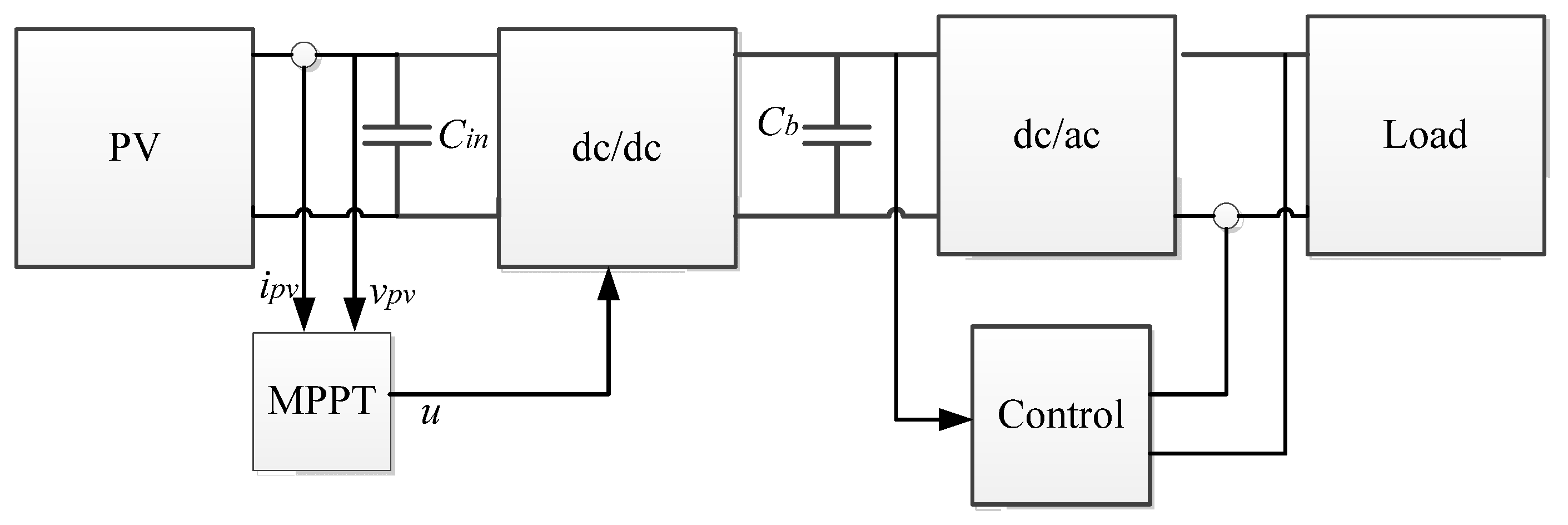
i.e., the optimal operation condition) known as Maximum Power Point Tracking (MPPT) algorithm. The classical structure of a grid-connected photovoltaic system is presented in
Figure 1, in which the PV generator interacts with a DC/DC converter controlled by a MPPT algorithm [
2,
3]. Such a structure enables the PV system to modify the operation conditions in agreement with the environmental circumstances (mainly changed by the irradiance and temperature) so that a maximum power production is achieved [
4,
5].
Figure 1 also illustrates the gird-connection side of the PV system, which is formed by a DC-link (capacitor
Cb) and a DC/AC converter (inverter). The inverter is controlled to follow a required power factor, provide synchronization and protect against islanding, among others. Moreover, the inverter must to regulate the DC-link voltage at the bulk capacitor
Cb, where two cases are possible: first, the inverter regulates the DC component of
Cb voltage, but due to the sinusoidal power injection into the grid,
Cb voltage experiments a sinusoidal perturbation at twice the grid frequency and with a magnitude inversely proportional to the capacitance [
3]. In the second case, the DC component of
Cb voltage is not properly regulated, which produces multiple harmonic components with amplitude inversely proportional to the capacitance [
3]. In both cases, the DC/DC converter output terminals are exposed to voltage perturbations that could be transferred to the PV generator terminals, thus degrading the MPP tracking process. Concerning the DC/DC power converter, the boost topology is the most widely used due to the low voltage levels exhibited by commercial PV modules [
6].
Figure 1.
Typical structure of a photovoltaic (PV) system.
Figure 1.
Typical structure of a photovoltaic (PV) system.
Multiple types of MPPT solutions are reported in the literature, which differ in complexity, number of sensors needed for operation, convergence speed, cost-effective range,
etc. [
7]. Two of the most commonly used MPPT techniques are Perturb and Observe (P & O) and Incremental Conductance (IC); the reason for this popularity is its implementation simplicity and its relatively good performance [
4,
8]. Other MPPT techniques are based on using fractional values of the open circuit voltage and short circuit current,
i.e., the Fractional Open Circuit Voltage and the Fractional Short-Circuit Current. The main advantages of those solutions are the low cost and implementation simplicity since they only require a single (voltage or current) sensor [
9,
10]; But their efficiency is low compared with the P & O and IC algorithms. In contrasts, techniques based on computational intelligence, such as neural networks and fuzzy logic, offer speed and efficiency in tracking the MPP [
11,
12,
13]; however its complexity and implementation costs are high compared with the P & O and IC algorithms, which make them costly solutions.
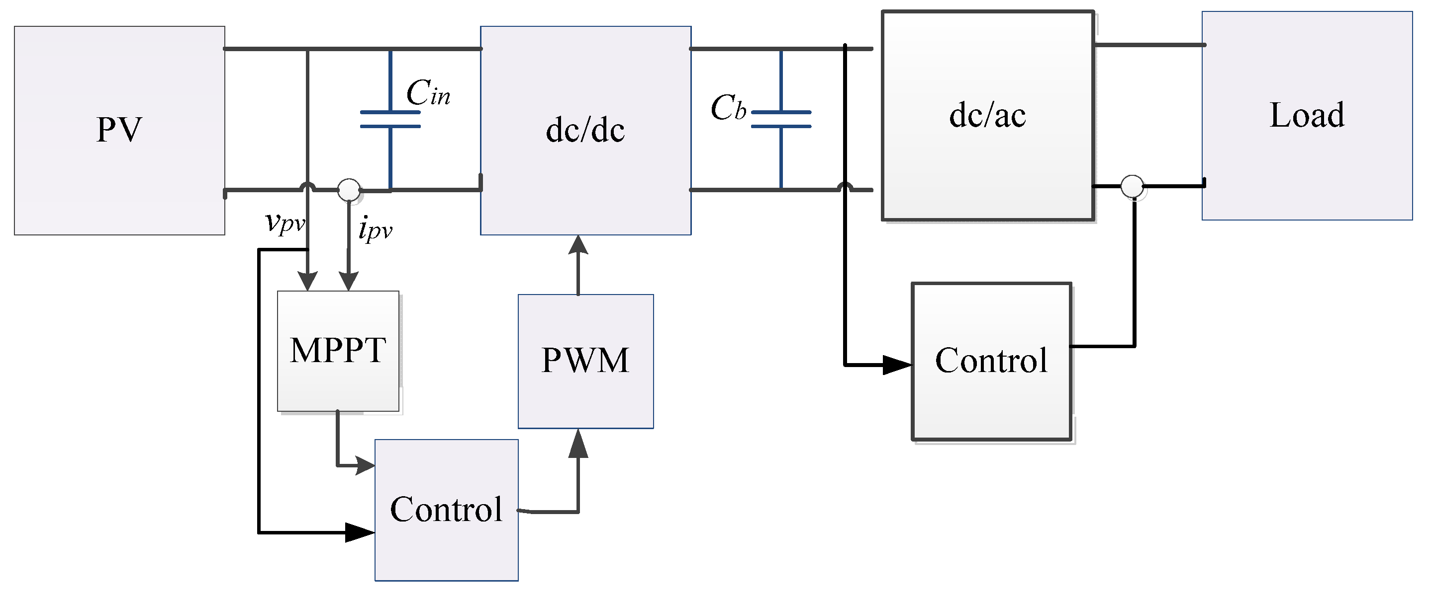
The main problem of using traditional MPPT algorithms acting on the duty cycle of the DC/DC converter associated to the PV generator,
i.e.,
Figure 1, concerns the large disturbances caused by irradiance transients in the system operating point, which generates a slow tracking of the MPP. This condition is also present at the system start-up, in which the MPPT algorithm takes a large amount of time to reach the MPP [
3]. To mitigate such disturbances and speed-up the MPPT procedure, a two-stage control structure is usually adopted: it generally involves an algorithmic MPPT controller in cascade with a conventional voltage regulator (e.g., based on lineal or nonlinear control) as depicted in
Figure 2. Moreover, such a structure is also needed to increase the reliability of double-stage grid-connected PV systems: the sinusoidal oscillation on the DC-link caused by the inverter operation must be mitigated, otherwise the MPPT procedure could be inefficient as reported in [
3]. Such mitigation is traditionally performed by using large electrolytic capacitors for
Cb, however the electrolytic technology introduces reliability problems due to its high failure rate [
14]. Then, the voltage regulator in
Figure 2 enables to mitigate the voltage oscillations in the DC-link produced by small non-electrolytic capacitors, thus improving the system reliability [
3,
14].
Figure 2.
Structure of a PV system with a classical pulse width modulation (PWM)-based cascade control.
Figure 2.
Structure of a PV system with a classical pulse width modulation (PWM)-based cascade control.
However, the design process of such a voltage regulator depends on the MPPT parameters, while the MPPT controller stability also depends on the cascade controller performance [
3]: for example, to ensure the stability of a P & O algorithm, its perturbation period must be larger than the settling time of the PV voltage, which depends on the system operating point and on the cascade voltage controller. However, the voltage controller design requires performance criteria, e.g., the settling time as in [
3], which are usually imposed in terms of the P & O parameters. Such a circular dependency in the two controllers design makes difficult to guarantee both system stability and desired performance in all the operating conditions.
When the voltage regulator is implemented using conventional linear control techniques it is necessary to linearize the system model around a given operation point, which is usually the MPP at some irradiance condition [
3]. However, due to the nonlinear nature of the PV module and DC/DC converter, the performance (and even stability) of the linear controller is limited to the neighborhood around the MPP [
15]. This constraint puts at risk the system performance since the operating point changes with the unpredictable and unavoidable environmental perturbations. To address this problem, the work in [
16] uses a sliding mode controller (SMC) to regulate the inductor current of a boost converter associated to the PV module, which enables to guarantee global system stability at any operating point. The solution proposed in that work considers three controllers in cascade as follows: the SMC that generates the activation signal for the MOSFET, a PI controller designed to provide the SMC reference depending on the command provided by a P & O algorithm, which is in charge of optimizing the power. However, the design of the PI controller requires a linearized model of the system around the MPP, hence it cannot guarantee the same performance in all the range of operation. In fact, a wrong design of such a PI controller could make the P & O unstable, hence both PI and P & O controllers have a circular dependency on their parameters. Similarly, the work in [
17] uses a SMC to regulate the input capacitor current of the boost converter. This solution has a major advantage over the work reported in [
16]: the solution in [
17] does not require a linearized model since the transfer function between the capacitor current and voltage is linear and it does not depend on the irradiance or temperature conditions. Therefore, such a solution is able to guarantee the desired performance in all the operating range. However, as in the previous work, the three controllers are designed separately, which makes difficult to perform the system design: again, a wrong P & O perturbation period could lead to an unstable system operation.
To avoid the circular dependency between voltage controllers and MPPT algorithms, a single controller in charge of both MPPT and voltage control operations is required. This problem has been addressed in [
18,
19,
20,
21] by using the sliding mode control technique. However, those works are based on two considerations difficult to apply to grid-connected PV systems: First, there is not considered a capacitor linking the PV array and the DC/DC converter; second, the load impedance is considered constant.
Regarding the first consideration, PV systems commonly consider a capacitor between the PV source and the DC/DC converter to stabilize the PV voltage, which in turns stabilizes the power produced, otherwise the current ripple at the DC/DC converter input will produce undesired oscillations that will degrade the MPPT procedure. The worst case of that current ripple is exhibited by DC/DC converters with discontinuous input current, e.g., buck or buck-boost topologies, while DC/DC converters with continuous input current only inject the inductor current ripple, e.g., boost, Sepic or Cuk topologies. In any case, a capacitor in parallel with the PV source is almost always considered; in fact, the experimental scheme of [
21] includes such a capacitor despite it is not taken into account for the SMC analysis. It must be noted that this capacitor defines the dynamic behavior of the PV voltage and power, therefore it must be considered in the PV controller design.
Regarding the second consideration, which assumes constant the load impedance, it is not applicable to grid-connected inverters since, as reported in [
22], such inverters are controlled to provide a constant average value in the DC-link, with sinusoidal oscillations at twice the grid frequency due to the injection of single-phase AC power. Therefore, the best representation of such a load (from the DC/DC converter side) is a voltage source and not a constant impedance. This model will be further justified in
Section 2. Therefore, in the design of a PV controller for grid-connected applications it is desirable to account for loads with non-constant impedance.
Other interesting sliding-mode controller for PV systems is presented in [
23], it considering a buck converter. Despite this work considers the capacitor linking the PV source and the power stage, it is not applicable to grid-connected PV systems since the DC/DC converter provides an output voltage lower than the one provided by the PV source. Such a condition is incompatible with the high input-voltage required by classical buck inverters for grid-connection [
22,
24]. Moreover, this work also assumes constant the load impedance, and it does not analyze the switching frequency, which is an important parameter for implementation.
On the basis of those previous works and considerations, this paper presents the analysis and design of a SMC aimed at performing a fast MPPT action on grid-connected PV systems using a single control stage. This approach avoids the circular dependency among cascade controllers, reduces the number of controllers and avoids the use of linearized models to provide global stability in all the operation range. In such a way, even the use of a PWM is not needed. Such a compact design also reduces the system cost and complexity.
The paper is organized as follows:
Section 2 presents the non-linear mathematical model representing the PV system, then
Section 3 introduces the proposed sliding surface and the controller structure.
Section 4 presents the mathematical analysis of the transversality, reachability and equivalent control conditions to demonstrate the global stability of the proposed controller. Finally,
Section 5 illustrates the performance of the proposed solution using detailed simulations executed in a standard power electronics simulator. The conclusions close the paper.
2. System Model
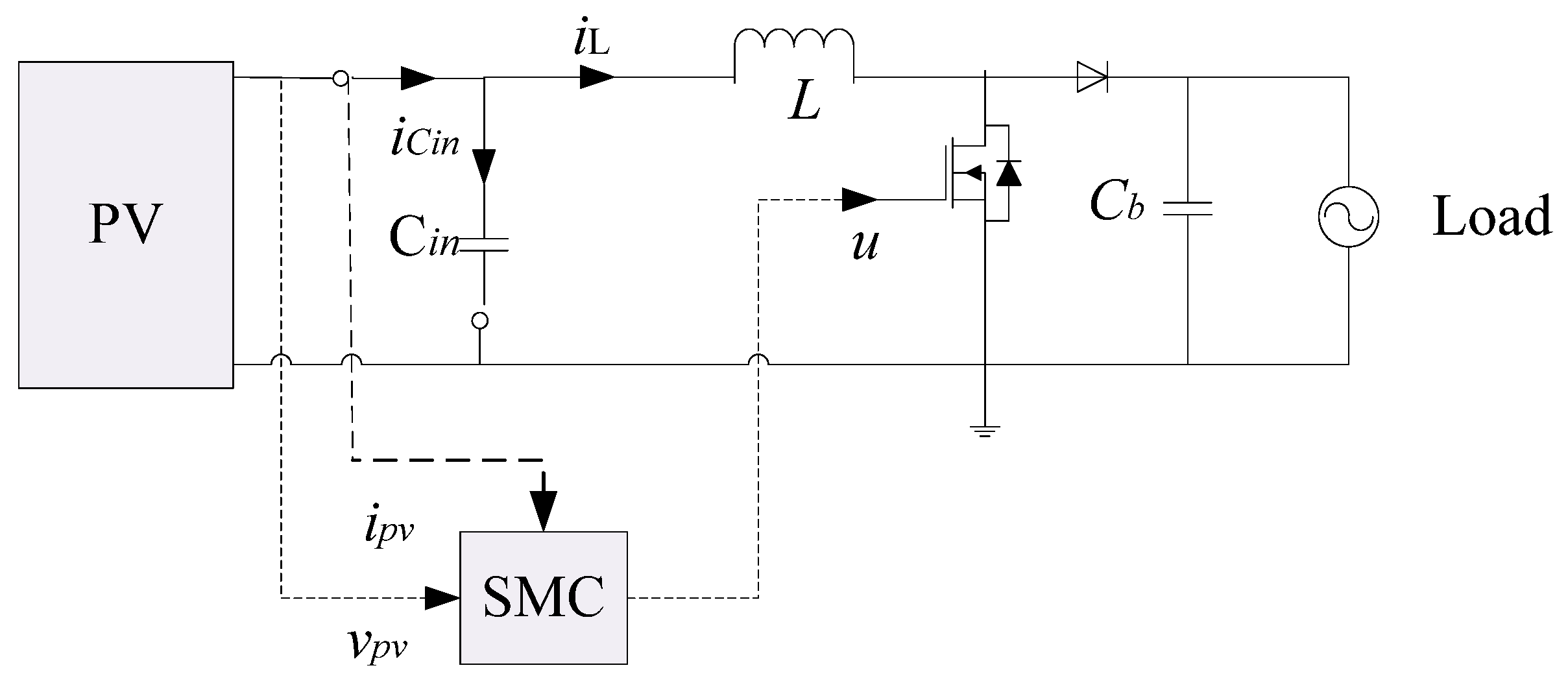
A simplified circuital scheme of the PV system is presented in the
Figure 3, which considers a boost converter due to the widely adoption of such a step-up DC/DC structure in PV systems, however the analysis presented in this paper can be extended to other DC/DC topologies. The scheme includes a voltage source as the system load, this to model the DC-link of double-stage structures in commercial PV inverters, in which the DC/AC stage regulates the DC-link voltage (
Cb capacitor voltage) [
25]. This voltage source model is widely used to represent the closed-loop grid-connected inverters due to its satisfactory relation between accuracy and simplicity, which is confirmed in references [
3,
17,
25,
26,
27,
28,
29].
The scheme considers the SMC acting directly on the MOSFET by means of the signal
u, which is a discontinuous variable. Hence, no linearization or PWM are needed. This condition reduces the implementation cost, and circuit complexity, in comparison with SMC solutions implemented with PWM circuits, e.g., [
21].
Figure 3.
Circuital scheme of the sliding mode controller (SMC) loop.
Figure 3.
Circuital scheme of the sliding mode controller (SMC) loop.
The dynamic behavior of the DC/DC converter is modeled by the switched Equations (1) and (2) [
30], where
iL represents the inductor current,
vpv is the PV voltage,
ipv represents the PV module current,
vb is the load voltage and
L and
Cin represent the inductor and capacitor values:
The current of the PV module is modeled with the simplified single diode model [
17] given in Equation (3). In such a model
isc represented the short-circuit current that is almost proportional to the irradiance [
17],
B is the diode saturation current and
A represents the inverse of the thermal voltage that depends on the temperature [
25]. Such a model parameters are calculated as
,
and
, where
istc and
Tstc are the short-circuit current and temperature of the module under standard test conditions (STC), respectively.
voc represents the open-circuit voltage, while
vMPP and
iMPP correspond to the PV voltage and current, respectively, at the MPP for the given operating conditions. Finally,
av is the voltage temperature coefficient [
31]:
In conclusion, the non-linear equations system formed by Equations (1)–(3) describes the PV system dynamic behavior in any operation condition.
3. Sliding Surface and Controller Structure
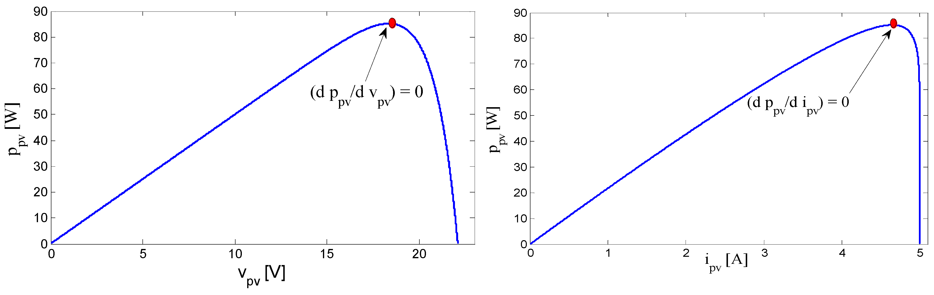
The non-linear relation between the PV current and voltage, given in Equation (3), produces a non-linear relation between the PV power and voltage (or current), which exhibits a maximum as depicted in
Figure 4. In such a maximum,
i.e., the MPP, the derivative of the power with respect to the voltage (or current) is zero as given in Equation (4). Therefore, the sliding-mode controllers proposed in [
18,
19,
20,
21,
23] are based on Equation (4). In a similar way, this paper proposes a sliding surface based on Equation (4):
Figure 4.
Power curves of a PV module.
Figure 4.
Power curves of a PV module.
Taking into account that
ppv =
vpv.
ipv, the following relation holds at the MPP:
Then, the following relation defines the maximum power condition,
i.e., at the MPP:
To correlate the MPP condition Equation (4) with the time-varying signals of the DC/DC converter, the condition in Equation (6) is expressed in terms of the time derivatives of both the PV voltage and current, obtaining expression Equation (7):
From such an expression, the proposed switching function Ψ and sliding surface Φ, given in Equation (8), are defined:
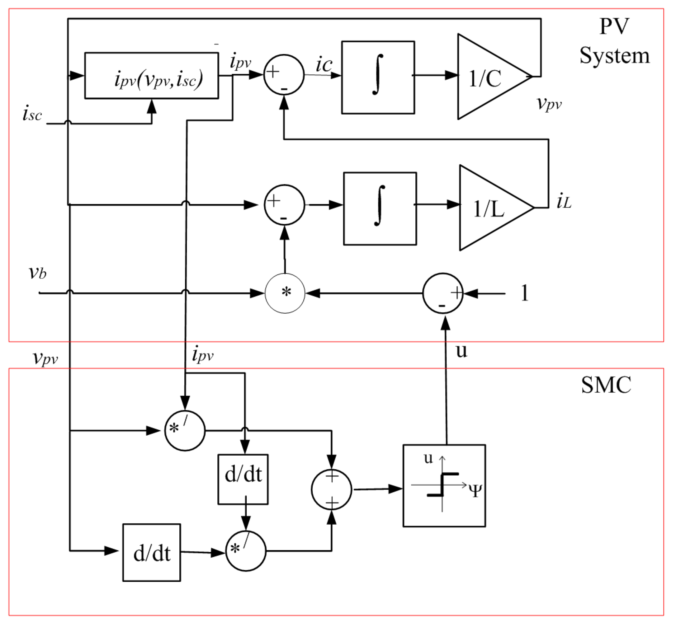
Then, the state-space model of both the PV system and SMC is formed by the simultaneous Equations (1)–(3) and (8). The relations within such a state-space model are illustrated in the block diagram of
Figure 5, which put in evidence the signals processing and variables exchanged between the PV system and the SMC: the PV system disturbances are the short-circuit current (defined by the irradiance and temperature) and the load voltage; the control signal
u is generated by the SMC on the basis of the PV current and voltage; and the SMC derives both the PV voltage and current to construct the switching function. Finally, the SMC includes a comparator to implement the sign function that triggers the changes on the signal
u. The design of such a comparator is described in the following section in terms of the transversality and reachability conditions.
Figure 5.
Block diagram of the SMC and PV system.
Figure 5.
Block diagram of the SMC and PV system.
4. Analysis of the Sliding-Mode Controller
The SMC must fulfill three conditions to guarantee stability and a satisfactory performance: transversality, reachability and equivalent control [
32]. The transversality analyses the controllability of the system, the reachability analyses the ability of the closed-loop system to reach the surface, and the equivalent control grants local stability.
Those conditions grant the existence of the sliding-mode, which also imposes the conditions defined in Equation (9) [
33]:
Such expressions provide information concerning the surface and its derivative. In that way, the derivate of the switching function is given in Equation (10):
To analyze expression Equation (10) it is required to also derive expressions Equations (2) and (3), it leading to expressions Equations (11)–(13), which are components of Equation (10):
Then, the small-signal admittance of the PV module
is introduced into the previous equations to provide more compact expressions:
Replacing Equations (1) and (14)–(16) into Equation (10), and performing some mathematical manipulations, the following expression for the switching function derivate is obtained:
This new expression is used to analyze the transversality, reachability and equivalent control conditions in the following subsections.
4.1. Transversality Condition
To ensure the ability of the controller to act on the system dynamics, the transversality condition given in Equation (18) should be granted [
33]:
Deriving Equation (17) with respect to the signal
u leads to expression Equation (19):
The analysis of Equation (19) requires to review the condition in which the MPP occurs: taking into account that
ppv = vpv · ipv, condition Equation (4) corresponds to expression Equation (20). Therefore, expressions Equations (18) and (19) lead to the transversality condition Equation (21):
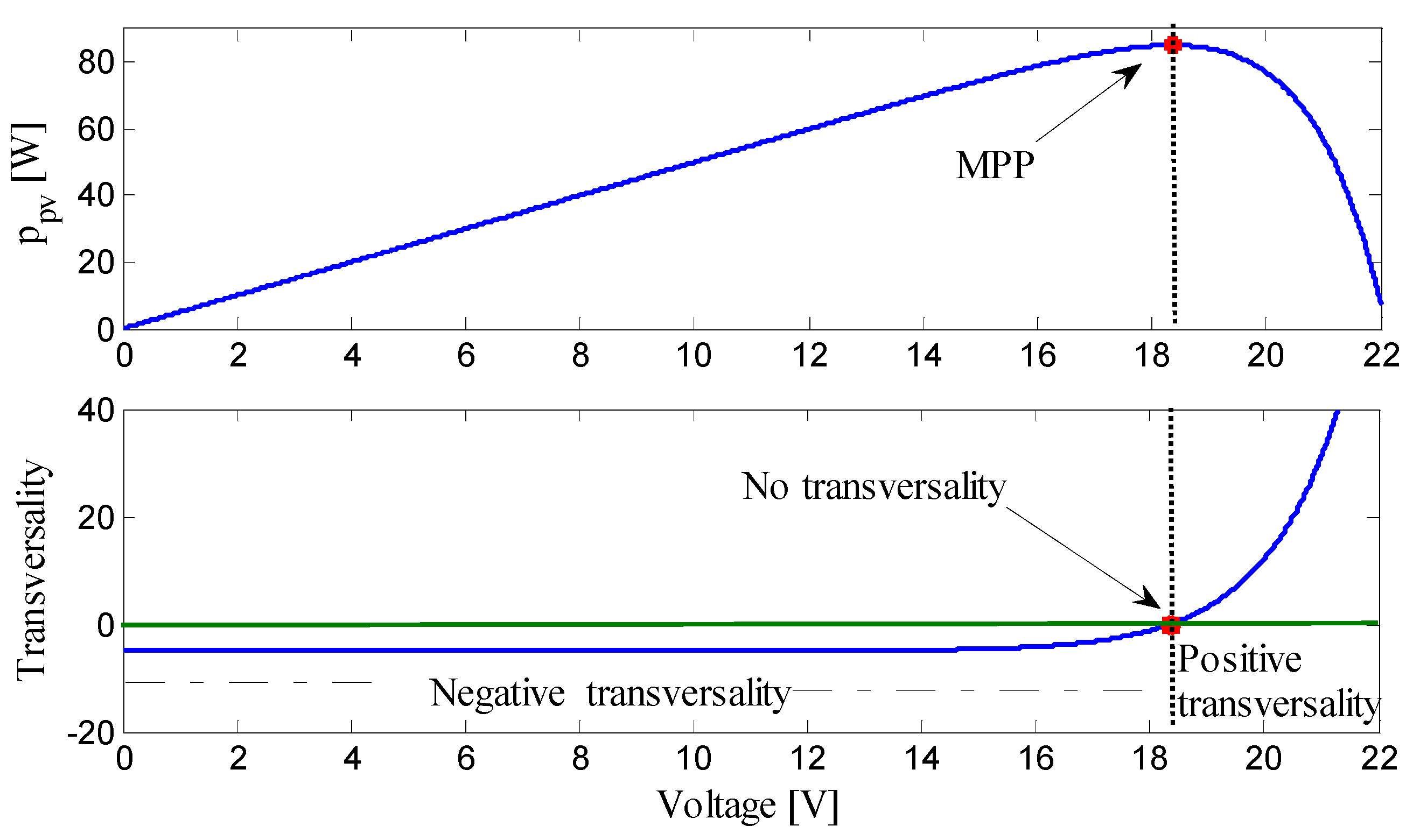
Figure 6 shows the simulation of Equation (19) considering the following conditions: a BP585 PV module with parameters
B = 0.894 μF and
A = 0.703 V
−1, and a DC/DC converter with
L = 100 μH,
Cin = 44 μF and
vb = 24 V. The simulation illustrates the transversality condition provided by Equation (21):
At the left of the MPP (voltages lower than vMPP) the transversality condition is fulfilled, hence the SMC is able to act on the PV system to drive it towards the MPP.
At the right of the MPP (voltages higher than vMPP) the transversality condition is also fulfilled.
At the MPP (vpv = vMPP) the transversality condition is not fulfilled. This is not a problem because the PV system is already at the MPP. Moreover, if the system diverges from the MPP the transversality condition is fulfilled.
Figure 6.
Simulation of the transversality condition.
Figure 6.
Simulation of the transversality condition.
The previous conditions impose a behavior similar to the classical hysteresis implementation of the SMC for DC/DC converters: the system oscillates around the surface forming a hysteretic trajectory. In the following subsections it will be demonstrated that such hysteresis band is imposed by the peak-to-peak amplitude of the voltage ripple at the PV module terminals.
4.2. Equivalent Control Condition
The equivalent control condition analyzes the ability of the system to remain trapped inside the surface [
31,
32]. This condition is analyzed in terms of the equivalent analog value
ueq of the discontinuous control signal
u: if such an equivalent value is constrained within the operational limits the system will not be saturated and its operation inside the surface is possible. Since the control signal u corresponds to the MOSFET activation signal, its operational limits are 0 and 1. Moreover, since the analysis considers the system inside the surface, the condition
holds. Then, matching expression Equation (17) to zero, and replacing
u =
ueq, enables to obtain the
ueq value given in Equation (22):
Such an expression can be rewritten as Equation (23), where
u1 and
u2 are given in Equations (24) and (25), respectively:
The analysis of Equation (23) must be addressed by writing the derivative of Equation (8) in a different way as given in Equation (26):
Since the solar irradiance does not exhibit fast changes in comparison with the switching frequency of the converter, it is assumed constant (
) to simplify the analysis of Equations (17), (25) and (26), obtaining the simplified expressions Equations (27) and (28), respectively:
Taking into account that ipv ≠ 0 is a realistic condition since ipv = 0 does not occur at any MPP, the sliding-mode condition is reached in Equation (27) for . Then, replacing those conditions and ipv ≠ 0 into Equation (28) leads to u2 = 0.
Therefore, at low irradiance derivatives, expression Equation (23) for
ueq is approximately equal to
u1. To evaluate the validity of such an approximation,
ueq from Equation (23) was simulated at different irradiance derivatives and contrasted with
u1 from Equation (24): the first test considers a change from the highest irradiance possible on earth to a complete shade in 1 second,
i.e., 1 sun per second or dS/dt = 1 kW/(m
2 · s). The second test considers a derivative of 10 suns per s (dS/dt = 10 kW/(m
2 · s)), and the third test considers a derivative of 100 suns per s (dS/dt = 100 kW/(m
2 · s)), which is very large. The tests results are presented in the
Table 1, where it is observed that the error generated by assuming
ueq ≈
u1 is less than 1% for the case with the largest derivative, while the errors for the other cases are less than 0.1% and 0.01%.
Table 1.
Error presented at different irradiance changes.
Table 1.
Error presented at different irradiance changes.
| dS/dt | Error (%) = ((ueq − u1)/ueq × 100% |
|---|
| 1 kW /(m2. s) | 0.0075% < e < 0.008% |
| 10 kW /(m2. s) | −0.0912% < e < 0.04% |
| 100 kW /(m2. s) | 0.989% < e < 0.6883% |
Thus, the equivalent control analysis is based on expression Equation (29), which does not introduce a significant error:
Finally, since the equivalent control condition for a DC/DC converter application is 0 <
ueq < 1, such an expression is analyzed using the
ueq value given in Equation (29), which leads to expression Equation (30):
The condition in Equation (30) is always fulfilled since the analyzed PV system considers a boost converter. Therefore, the equivalent control is fulfilled.
4.3. Reachability Conditions
The reachability conditions analyze the ability of the system to reach the desired condition Ψ = 0. The work in [
32] demonstrated that a system that fulfills the equivalent control condition also fulfills the reachability conditions. That work also shows that the sign of the transversality condition imposes the value of
u for each reachability condition. A positive value of the transversality condition imposes the following reachability conditions:
Instead, a negative value of the transversality condition imposes the following reachability conditions:
Moreover, the reachability conditions define the implementation of the switching law [
32]. However,
Subsection 4.1 shows that the transversality condition in this SMC is both positive and negative depending on the operation condition. In such a way, from
Figure 6 it is observed that the voltage range for negative transversality (
vpv <
vMPP) is much larger than the voltage range for positive transversality (
vpv >
vMPP); therefore the implementation and analysis of the proposed SMC is performed in such a negative transversality condition, which imposes the following control law: {Ψ < 0 →
u = 0 ∧ Ψ > 0 →
u = 1}.
Then, the reachability of the surface is fulfilled in the following conditions:
with
u = 1 and
with
u = 0. Moreover, from Equation (27) it is observed that the sign of
is the same sign of
. Therefore, the analyzed reachability conditions are fulfilled in the following states:
The MOSFET is ON (u = 1) and the voltage is decreasing, i.e., .
The MOSFET is OFF (u = 0) and the voltage is increasing, i.e., .
It must be noted that a DC/DC converter always exhibits a periodic voltage ripple around an average value [
34]. In fact, the PV voltage corresponds to the voltage at the input capacitor
Cin in
Figure 3, which voltage ripple is defined by the second order filter formed by
Cin and the inductor
L. From the first differential equation of the DC/DC converter,
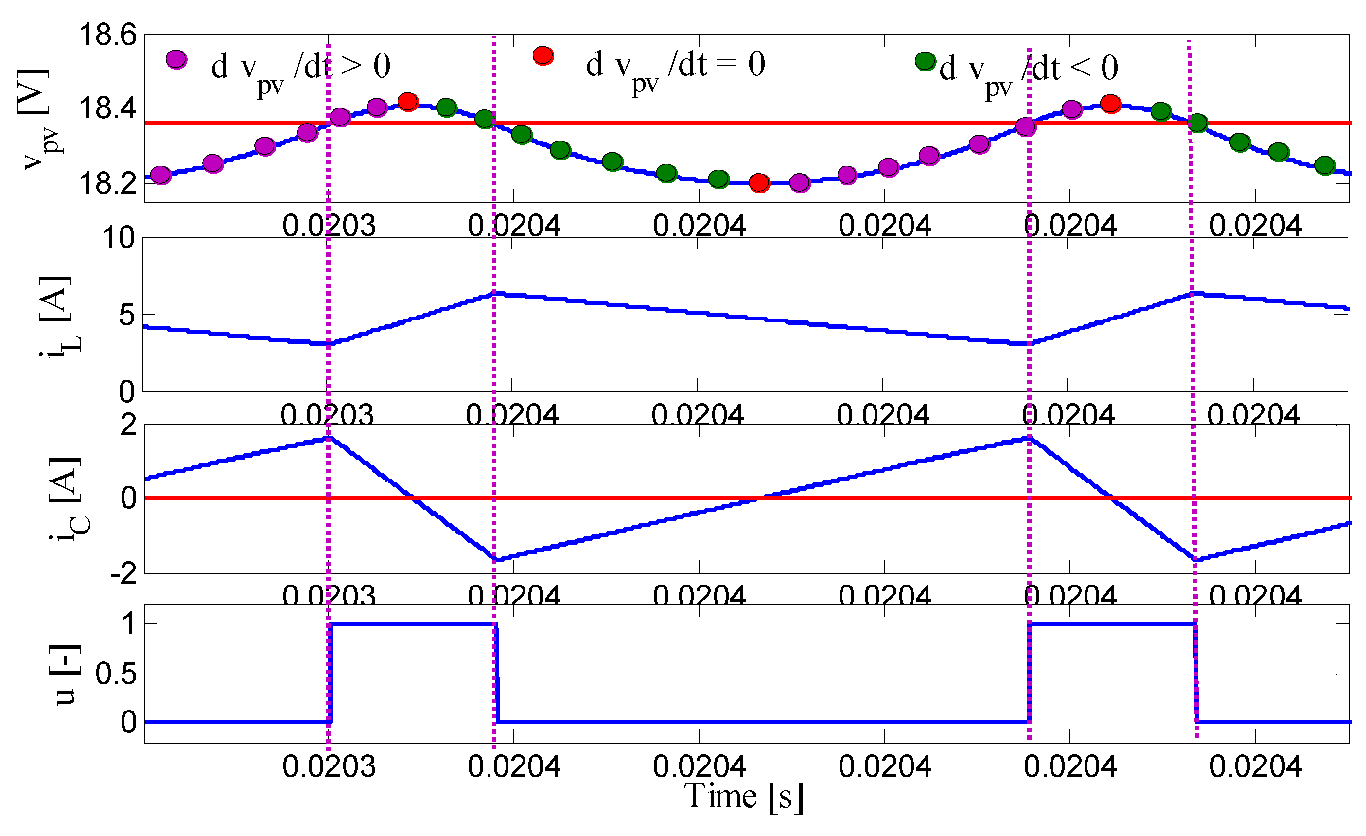
i.e., Equation (1), it is observed that the inductor current exhibits an almost triangular waveform as in any other second-order filter; hence in steady-state the capacitor current has a triangular waveform centered in zero, again as in any other second order filter [
30]. Therefore, the capacitor current increases with the MOSFET OFF (
u = 0). This behavior is observed in the simulation of
Figure 7, which includes the proposed SMC with the control action implemented as
u = 1 for Ψ < 0 and
u = 0 for Ψ > 0, and adopting the same electrical parameters previously described in
Subsection 4.1. The implementation of the SMC is described in
Section 5. The simulation also confirms that the capacitor current decreases with the MOSFET ON (
u = 1). Moreover, it is noted that with a constant value for
u (
u = 0 or
u = 1) the capacitor current exhibits positive, negative and zero values.
Figure 7.
PV system dynamic behavior.
Figure 7.
PV system dynamic behavior.
This means that, as reported by the second differential equation of the DC/DC converter,
i.e., Equation (2), the voltage ripple is a series of quadratic waveforms generated from the integral of the capacitor current since
iCin = ipv − iL. In such a way, the PV voltage exhibits positive and negative derivatives for both states of
u as reported in
Figure 7. Therefore, since the switching function derivative has the same sign of the PV voltage derivative, as reported in Equation (27), the reachability conditions are fulfilled in a fraction of the time intervals in which the MOSFET is in ON and OFF states, which means that in the other fractions of the time intervals the system diverges from the surface. Such conditions create a periodic behavior in which the system converges and diverges to/from the surface.
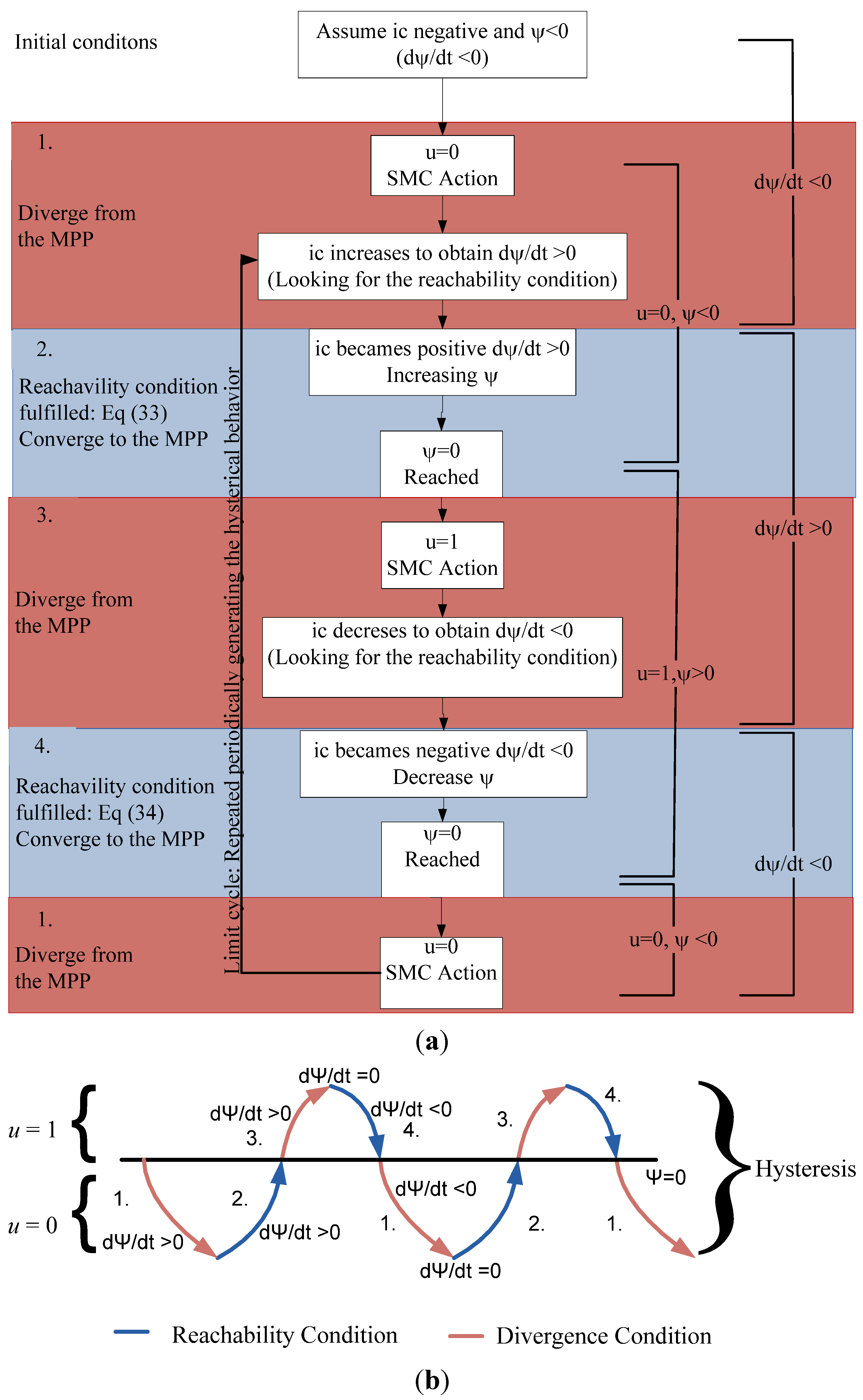
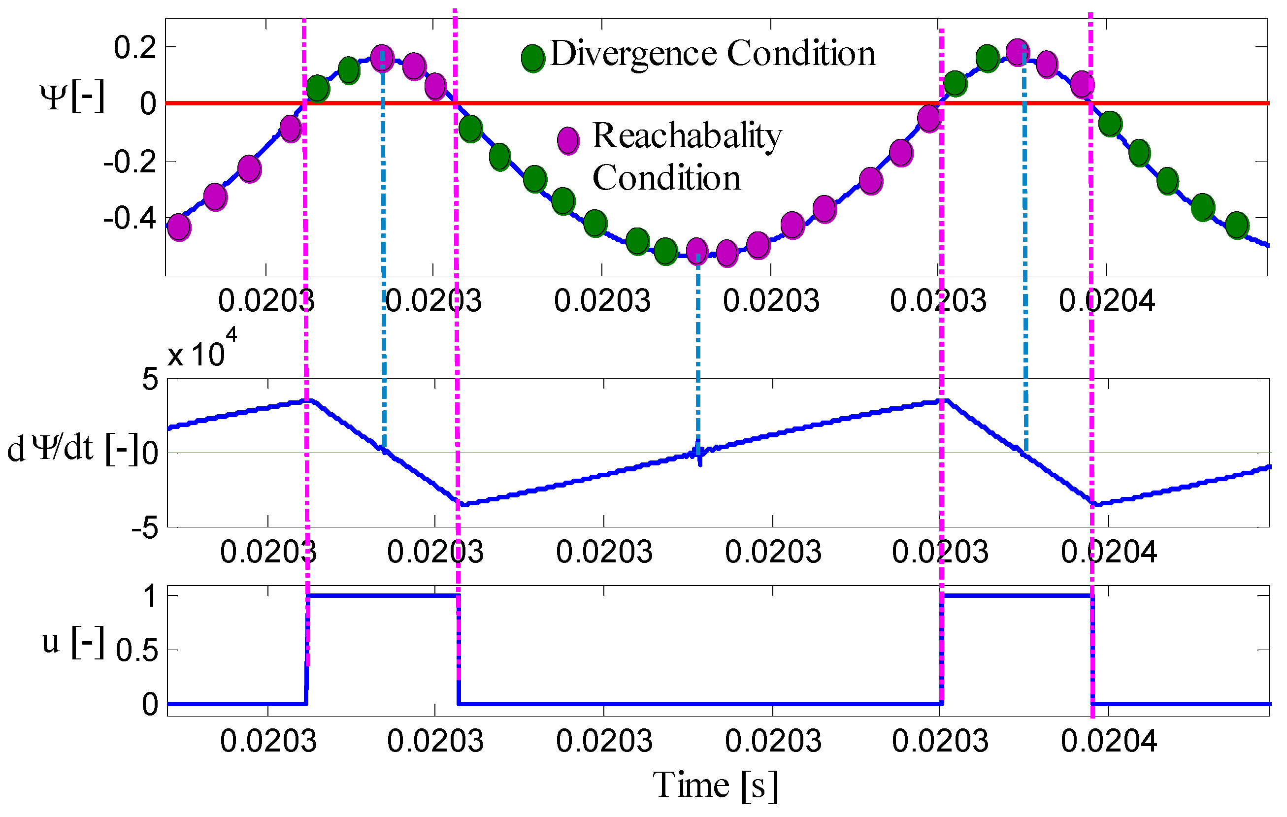
To illustrate the periodic behavior of the reachability conditions, and the resulting periodic behavior of the SMC,
Figure 8 shows two diagrams: A state flow describing the convergence and divergence states in
Figure 8(a), and the associated time-depending signal of the switching function in
Figure 8(b). For the sake of illustration, the system is considered at the beginning of the analysis under the surface,
i.e., Ψ < 0, and with a negative switching function derivative,
i.e.,
, which corresponds to a negative PV voltage derivative
as reported in Equation (27). Due to the differential equation governing the capacitor
, the condition
also corresponds to a negative input capacitor current,
i.e.,
. Those initial conditions are observed at the top of
Figure 8(a). Then, due to the control action implemented for the SMC, the control signal is set to
u = 0 and the system enters in the first state of operation:
Diverge from the MPP:
u = 0, Ψ < 0,
(
). In this first stage (block 1 in
Figure 8(a)) the reachability conditions are not fulfilled, hence the system diverges from the MPP, which is observed in
Figure 8(b). Such a condition is caused by the negative value of the switching function derivative, which reduces even more the value of Ψ, hence the desired condition Ψ = 0 is not achievable. However, the control action
u = 0 forces the increment of
, it driving the system to
(
) and eventually to
(
), which corresponds to the second stage of the SMC operation.
Converge to the MPP:
u = 0, Ψ < 0,
(
). In this second stage the reachability condition Equation (33) is fulfilled, hence the system converges to the MPP, which is also observed in
Figure 8(b). In this case, the positive value of the switching function derivative increases the value of Ψ, it driving the system towards the desired condition Ψ = 0. However, when the condition Ψ = 0 is reached the switching function derivative is still positive,
i.e.,
(
), hence
becomes positive. Moreover, when
the SMC imposes
, which corresponds to the third stage of the SMC operation.
Diverge from the MPP: u = 1, , (). In this third stage the reachability conditions are not fulfilled, hence the system diverges from the MPP. Such a condition is caused by the positive value of the switching function derivative, which increases even more the value of, hence the desired condition is not achievable. However, the control action forces the decrement of , it driving the system to () and eventually to (), which corresponds to the fourth stage of the SMC operation.
Converge to the MPP: , , ). In this fourth stage the reachability condition Equation (34) is fulfilled, hence the system converges to the MPP. In this case, the negative value of the switching function derivative decreases the value of , it driving the system towards the desired condition . However, when the condition is reached the switching function derivative is still negative, i.e., (), hence becomes negative. Moreover, when the SMC imposes u = 0, which corresponds to the first stage of the SMC operation.
Figure 8.
Periodic behavior of the reachability conditions. (a) Convergence and divergence conditions; (b) Hysteretic behavior.
Figure 8.
Periodic behavior of the reachability conditions. (a) Convergence and divergence conditions; (b) Hysteretic behavior.
The previous four stages of the system operation are continuously repeated, they form a limit-cycle [
35] that imposes a hysteretic behavior to the SMC switching function around the surface
. Moreover, from
Figure 8 it is noted that the hysteresis band is defined by the condition
, which corresponds to
and
as reported in Equation (27). This dependency is depicted in
Figure 7, and confirmed by
Figure 9, which presents
,
and
u generated by the same simulation producing the signals presented in
Figure 7. In addition,
Figure 9 also confirms the limit-cycle of the switching function. Finally, it is noted that the hysteresis band of the SMC is defined by the voltage ripple at the input capacitor, which can be modified by changing the input capacitance.
Figure 9.
SMC hysteretic behavior.
Figure 9.
SMC hysteretic behavior.
4.4. Switching Frequency
The switching frequency is an important parameter in the operation of DC/DC converters, hence it must be calculated in order to provide practical guidelines for the SMC implementation.
The switching frequency is calculated from the DC/DC converter differential equations and ripple magnitudes as reported in [
30]. In such a way, in a boost converter the ripple magnitude for the inductor current and capacitor voltage are given in Equations (35) and (36), respectively, where
Ts represents the switching period,
d represents the duty cycle, and
Fsw =1/Ts is the switching frequency:
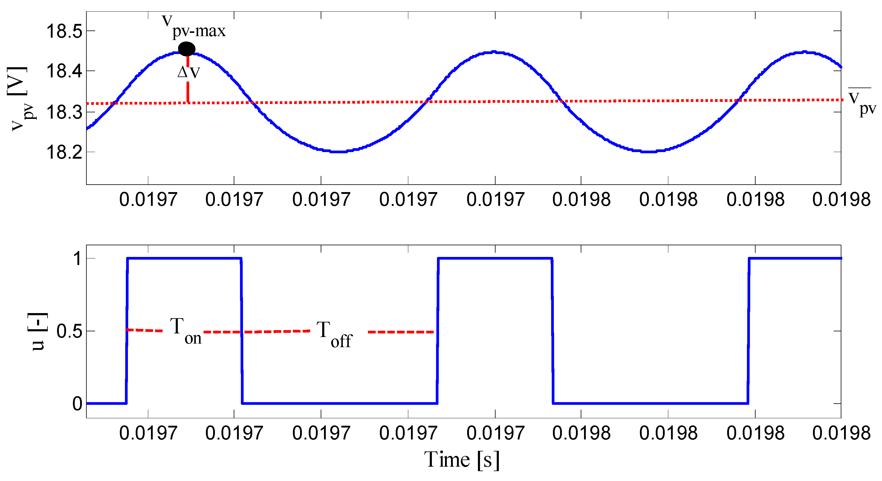
Figure 10 presents a simulation of the closed-loop SMC system highlighting the time intervals in which the MOSFET is turned on (T
on) and turned off (T
off). In such a figure it is observed that the magnitude of the voltage ripple
is mesured from the average PV voltage
to the peak (maximum) voltage
as
. Then, approximating the average PV voltage to the MPP voltage, the voltage ripple magnitude becomes
, where the MPP voltage is calculated from Equation (20) as
using the LambertW function [
36].
Figure 10.
Principle for calculating the switching frequency.
Figure 10.
Principle for calculating the switching frequency.
The maximum PV voltage
is achieved when
, which also corresponds to
and
u = 1 as demonstrated in the previous subsection. Then, replacing those values in Equation (17), and assuming
constant, Equation (37) is obtained:
Finally, replacing expressions Equations (35) and (37) into Equation (36) with
and
enables to calculate
as:
Similarly, taking into account that the minimum PV voltage
is achieved when
,
and
u = 0, the voltage ripple measured from
to the average PV voltage can be approximated as
. Then,
is calculated as in Equation (39), where d′ = 1−d represents the complementary duty cycle:
Finally, the switching frequency imposed by the SMC is given in Equation (40). In such an expression the duty cycle is evaluated as reported in Equation (35):
The accuracy of expression is illustrated by calculating the switching frequency of the PV system simulated in
Figure 10: Equation (40) predicts a switching frequency equal to 27.4 kHz, while the simulation reports a switching frequency equal to 28.41 kHz, which correspond to an acceptable prediction error of 3.5%.
Moreover, from expression Equation (40) it is evident that the switching frequency depends on the inductance and capacitance values, PV module characteristics and system operating point. Therefore, if or change due to aging or by other effects such as inductor saturation, the switching frequency will also change. However, the previous subsections demonstrate the robustness of the proposed SMC to changes in and : the system will remain stable for any positive values of and . In conclusion, tolerances in the converter parameters due to aging or practical saturations will not compromise the system stability.
4.5. Sliding-Mode Dynamics
The sliding-mode dynamics provide information concerning the averaged voltage and current behavior, which is useful to predict important time-based performance criteria such as settling time. The sliding-mode dynamics consider the system within the sliding surface, hence expressions Equation (7) hold, which leads to Equation (41):
Similarly, from the second differential equation of the DC/DC converter,
i.e., Equation (2), the relation
is obtained, which derivative is given in Equation (42):
Then, substituting Equations (1) and (41) into Equation (42), and naming the instantaneous PV module impedance
, the relation Equation (43) is obtained:
Expressing Equation (43) in Laplace domain leads to the model reported in Equation (44):
Such a second-order model describes the closed-loop system behavior around a given operation condition, in which the natural frequency is
and the damping ratio is
. From the classical second order system analysis [
37], the settling time of the PV voltage is, approximately,
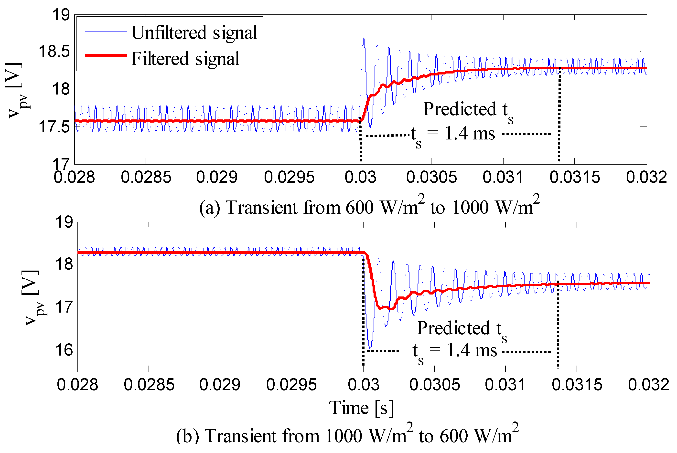
. To test such an estimation, the PV system controlled by the SMC, considering the parameters previously described in
Subsection 4.1, was simulated in both step-up and step-down irradiance transients. The first test considers a step change in the irradiance from 600 W/m
2 to 1000 W/m
2, which corresponds to a change in
isc from 3 A to 5 A, obtaining the results presented in
Figure 11(a): in such conditions the average PV module impedance is 5.1 Ω, which leads to t
s = 1.4 ms. To provide a more clear calculation of the settling time from the DC/DC converter waveforms, the PV voltage is also filtered to remove the switching ripple, which enables to verify the accuracy of the proposed approximation. Similarly, the second test considers a step change in the irradiance from 1000 W/m
2 to 600 W/m
2, obtaining the results presented in
Figure 11b, where the settling time estimation is the same,
i.e., t
s = 1.4 ms. Both simulations confirm the validity of the approximation. It must be noted that the settling time will change if
or
change, e.g., due to aging or practical saturations.
Figure 11.
Settling-time estimation.
Figure 11.
Settling-time estimation.
5. Numerical Results and Performance Evaluation
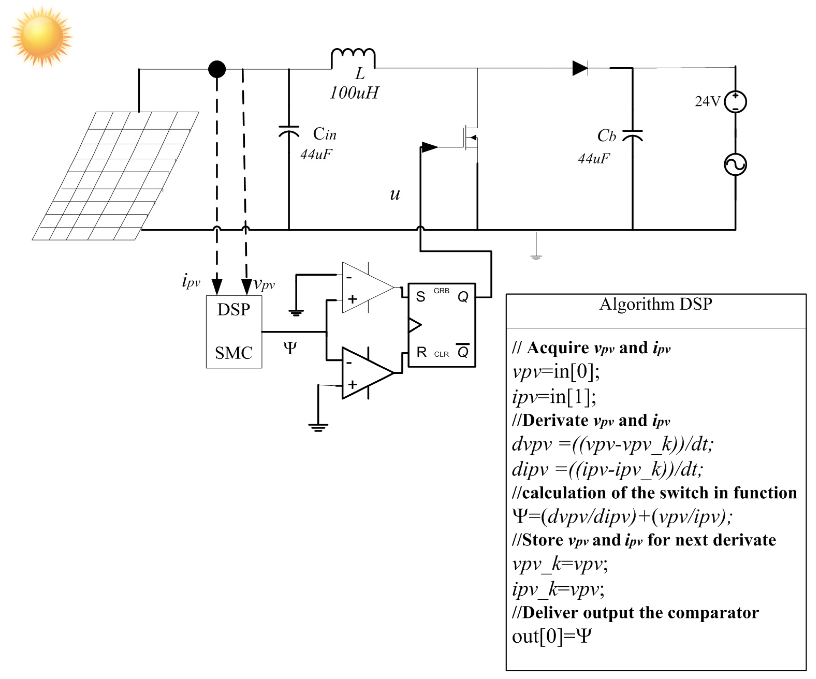
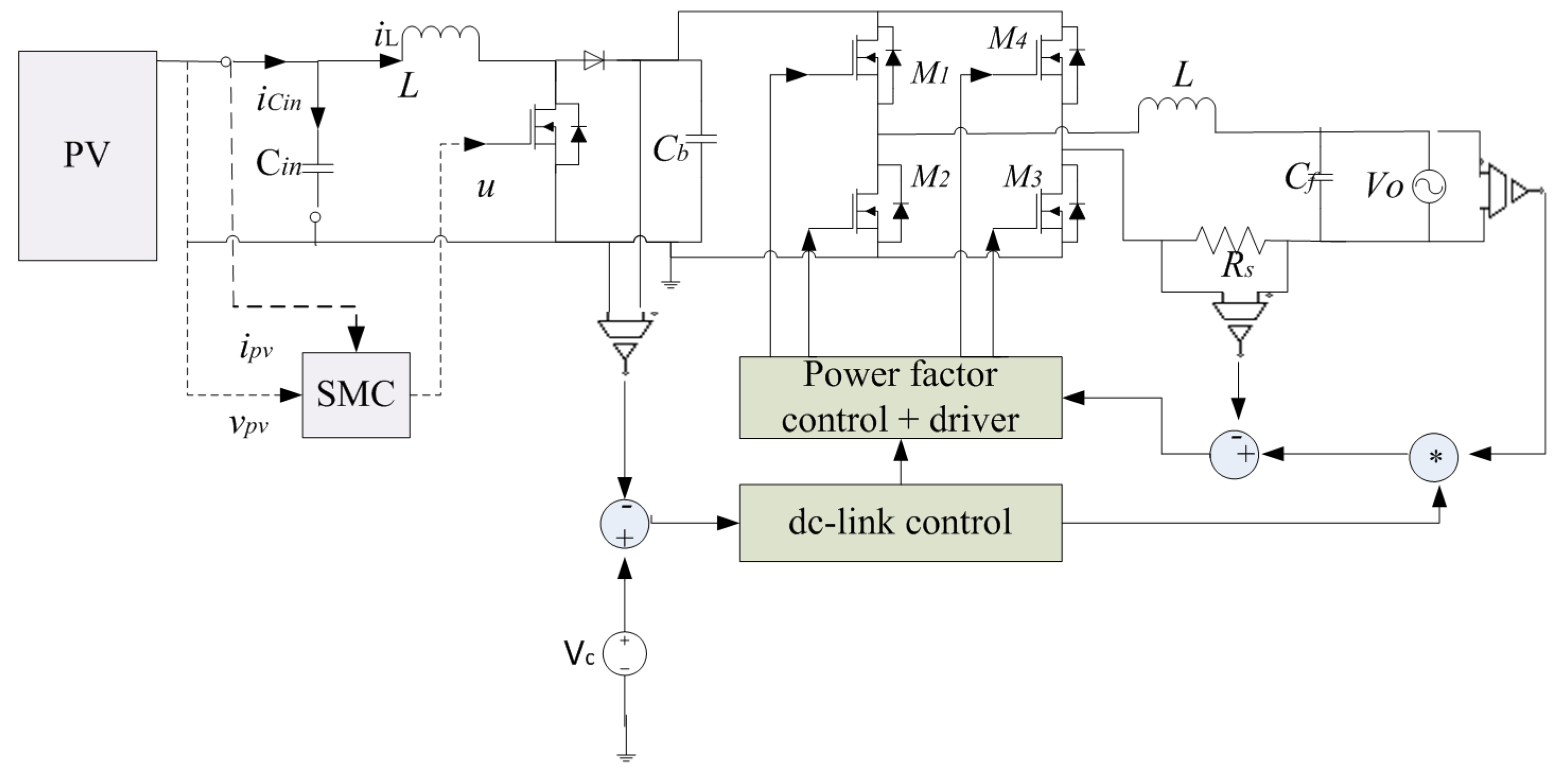
The proposed SMC was implemented in the power electronics simulator PSIM using C language. This procedure enables to tests, realistically, the performance of the SMC by emulating the implementation of the controller in a Digital Signal Processor (DSP). In addition, the ANSI C code used in the PSIM simulation (within a C block) can be directly executed in any DSP without major modifications.
Figure 12 presents the simulation scheme and SMC implementation, which uses four devices to implement the controller: a C block emulating the DSP, two classical comparators and a S-R flip-flop to store the
u signal. Such a structure is widely adopted in literature to implement the switching function due to its simplicity and reliability [
32]. However, since in this work the SMC performs both MPPT and voltage regulation actions, there is no need of cascade (or any other) controllers or modulators.
Figure 12 also presents the ANSI C code used to calculate the switching function, which is provided by using an emulated Digital-to-Analog Converter (DAC) to the switching circuit driving the MOSFET. To test the SMC in the same conditions used to illustrate the mathematical analysis, this simulation scheme considers a DC-link voltage near to 30 V imposed by the standard voltage source model representing the inverter. An additional simulation scheme will be used afterwards to test the SMC, under high boosting conditions, and interacting with a detailed grid-connected inverter.
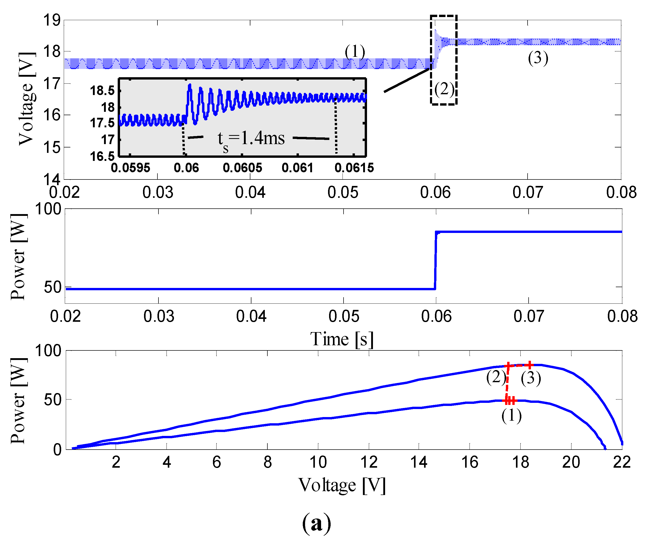
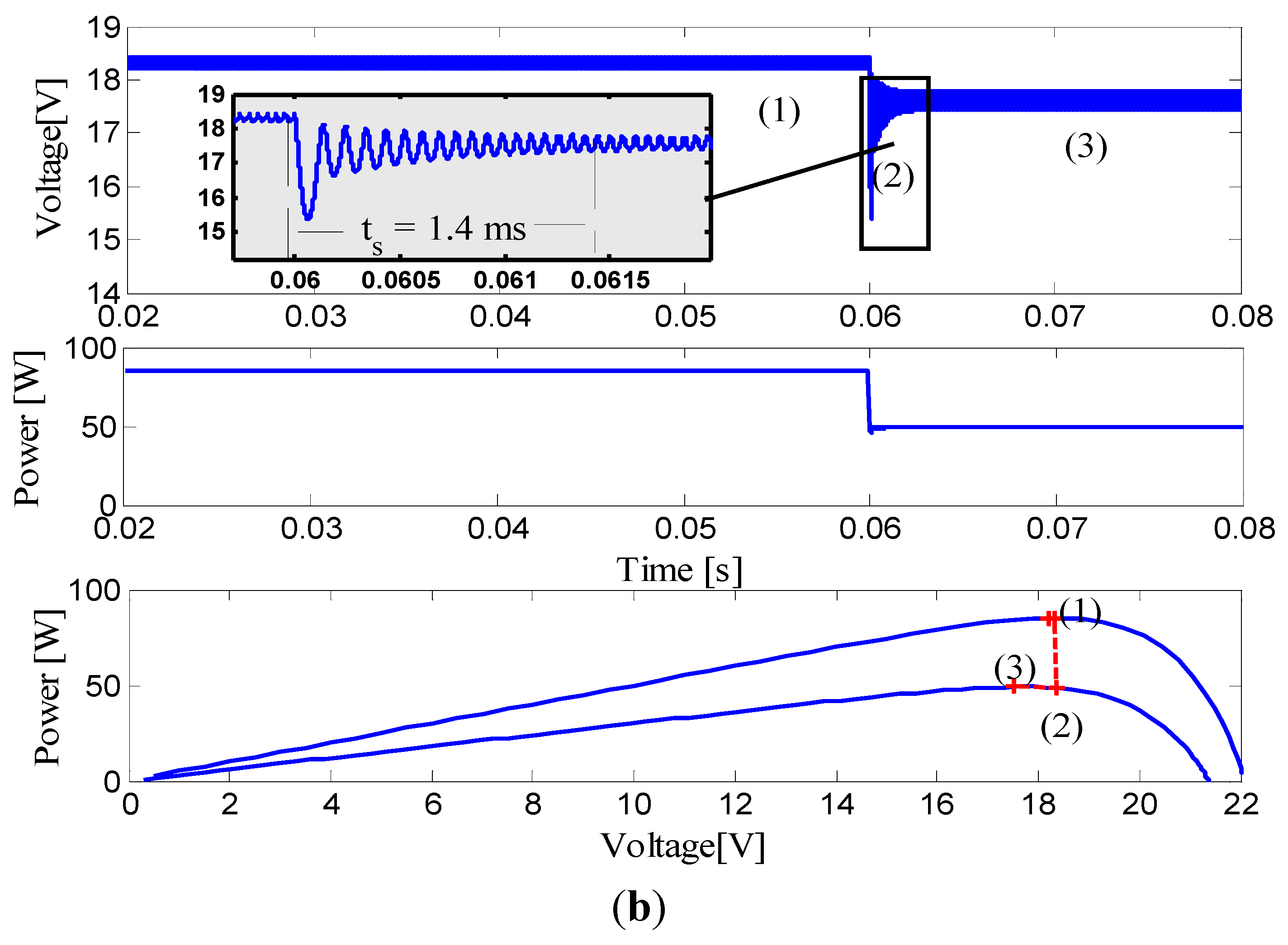
Figure 13 shows two tests performed in the first simulation scheme:
Figure 13(a) presents the dynamic response of the system for a change in the irradiance from 600 W/m
2 to 1000 W/m
2, while
Figure 13(b) presents the dynamic response of the system for a change in the irradiance from 1000 W/m
2 to 600 W/m
2. In both cases the SMC drives the PV system to the optimal operation condition within the estimated settling time. Moreover, such simulations also show the points in the I-V curve in which the PV system operates: (1) corresponds to the initial steady-state condition; then condition (2) is triggered by an irradiance perturbation; and (3) is the new MPP detected by the SMC.
Figure 12.
Simulation scheme and SMC implementation.
Figure 12.
Simulation scheme and SMC implementation.
Figure 13.
System Response to irradiance perturbations. (a) Transient from 600 W/m2 to 1000 W/m2; (b) Transient from 1000 W/m2 to 600 W/m2.
Figure 13.
System Response to irradiance perturbations. (a) Transient from 600 W/m2 to 1000 W/m2; (b) Transient from 1000 W/m2 to 600 W/m2.
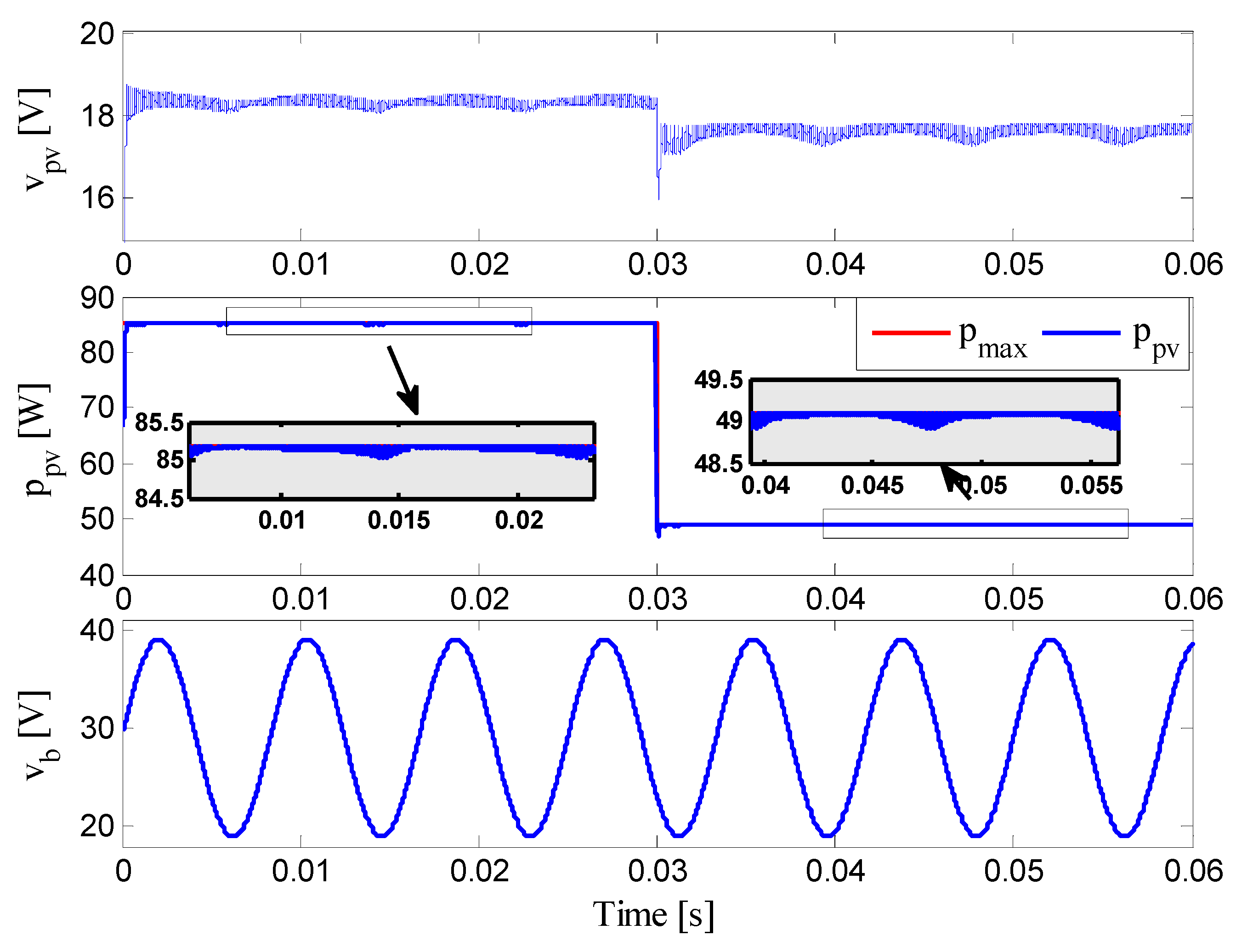
Taking into account that grid-connected PV systems exhibit perturbations at the DC-link, the SMC must be also tested in presence of sinusoidal voltage oscillations at
Cb. Such a test is presented in
Figure 14, where a large 20 V peak-to-peak voltage oscillation has been superimposed to a 29 V DC component, this corresponding to a 69% perturbation. The simulation also considers an irradiance perturbation from 1000 W/m
2 to 600 W/m
2 at
t = 0.03 s, and even under the perturbation in the load voltage the SMC is able to impose the expected behavior to reach the new MPP.
Figure 14.
System response with load perturbation.
Figure 14.
System response with load perturbation.
As anticipated before, a second simulation scheme is used to test the SMC under high boosting conditions and interacting with a detailed grid-connected inverter. Such a scheme is presented in
Figure 15 [
24], which includes a closed-loop inverter with two control objectives: provide a given power factor and regulate the DC-link voltage. The inverter is designed to operate at 110 VAC@60 Hz with an average DC-link voltage equal to 220 V. The DC-link is formed by
, which at 1000 W/m
2 experiment a large 120 V peak-to-peak voltage oscillation superimposed to the DC component, this corresponding to a 55% perturbation. Moreover, the input capacitor was changed to
to avoid large PV voltage oscillations due to the high voltage conversion ratio imposed to the DC/DC converter. Therefore, the SMC switching frequency, calculated from Equation (40), is approximately 100 kHz. In addition, the simulation also considers an irradiance perturbation from 1000 W/m
2 to 300 W/m
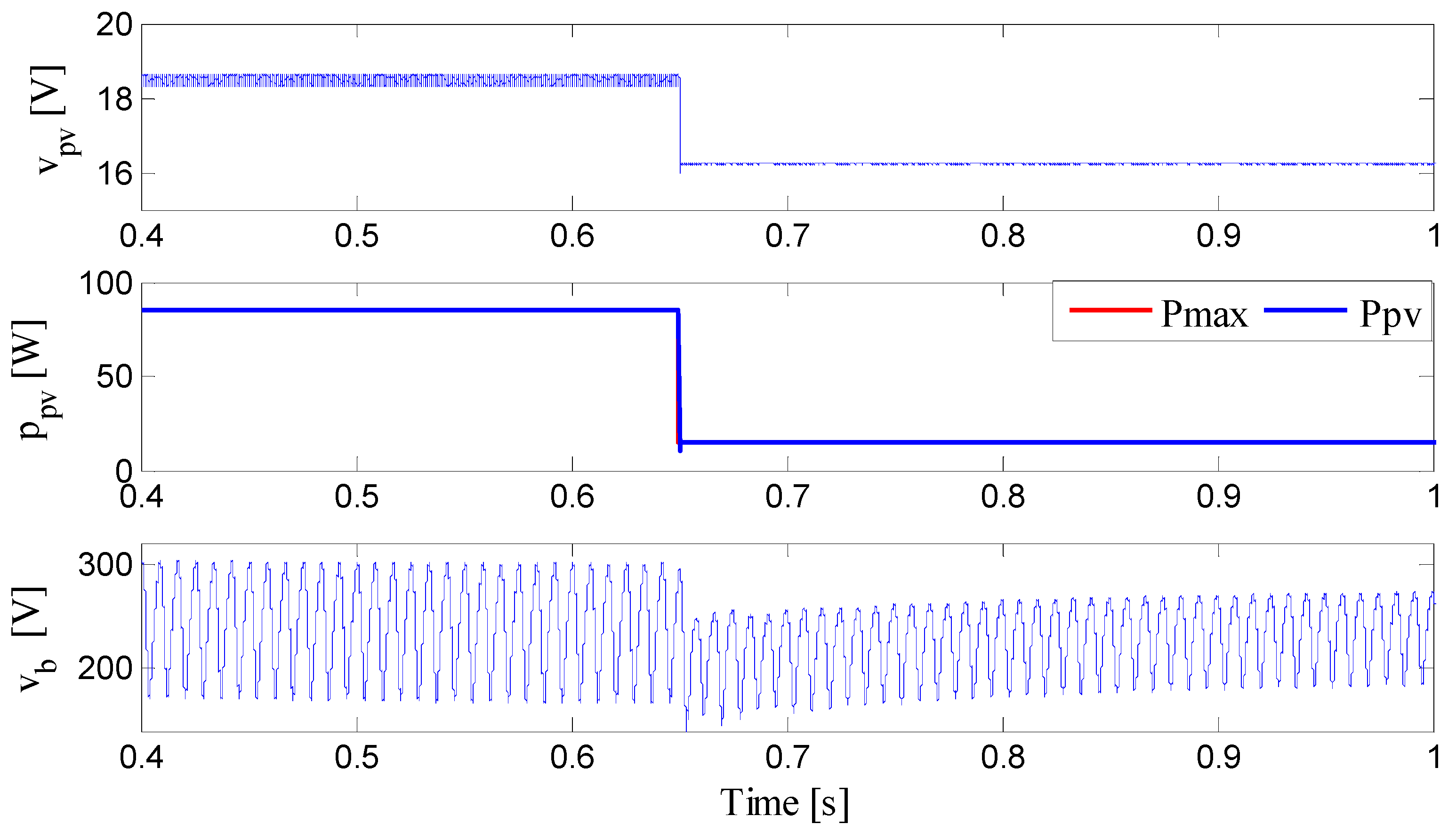
2 at t = 0.65 s to illustrate the MPPT operation of the SMC. The results are presented in
Figure 16, which confirms that even under high DC-link perturbations the SMC is able to reach the new MPP. It must be point out that the inverter also imposes a transitory behavior in the DC-link voltage due to the change in PV power at t = 0.65 s, which is also mitigated by the SMC.
Figure 15.
Circuital scheme of the detailed grid-connected PV system.
Figure 15.
Circuital scheme of the detailed grid-connected PV system.
Figure 16.
SMC behavior interacting with a grid-connected inverter.
Figure 16.
SMC behavior interacting with a grid-connected inverter.
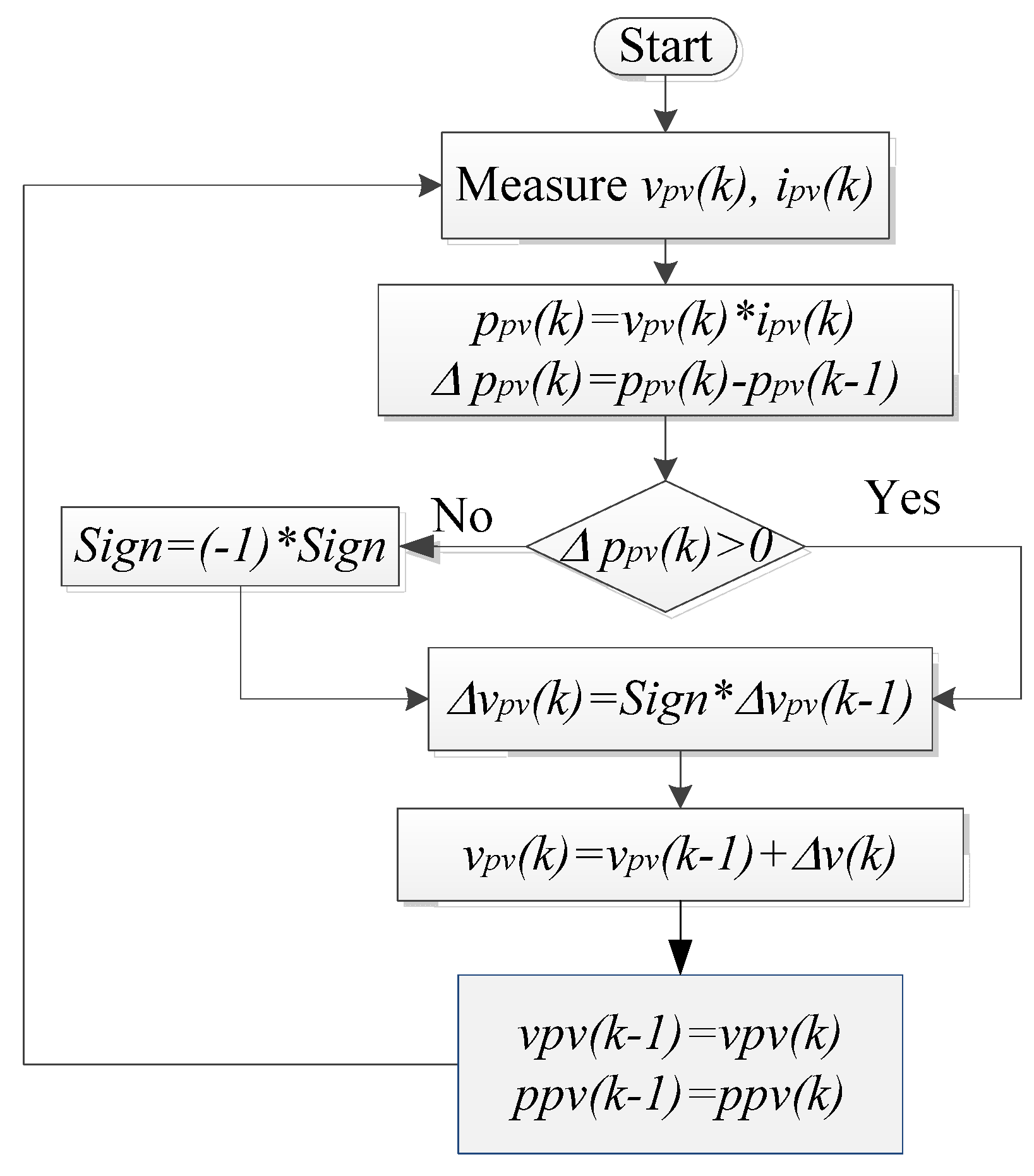
With the aim of further evaluate the proposed SMC, the performance of this controller is also contrasted with two classical solutions based on the P & O algorithm. The P & O method is based on perturb the input variable of the system, e.g., the duty cycle of the converter, observe the variation in the output power, and increase or decrease the perturbed variable to increase the power. The flowchart of the P & O algorithm is shown in
Figure 17.
Figure 17.
Flowchart of the Perturb and Observe (P & O) algorithm.
Figure 17.
Flowchart of the Perturb and Observe (P & O) algorithm.
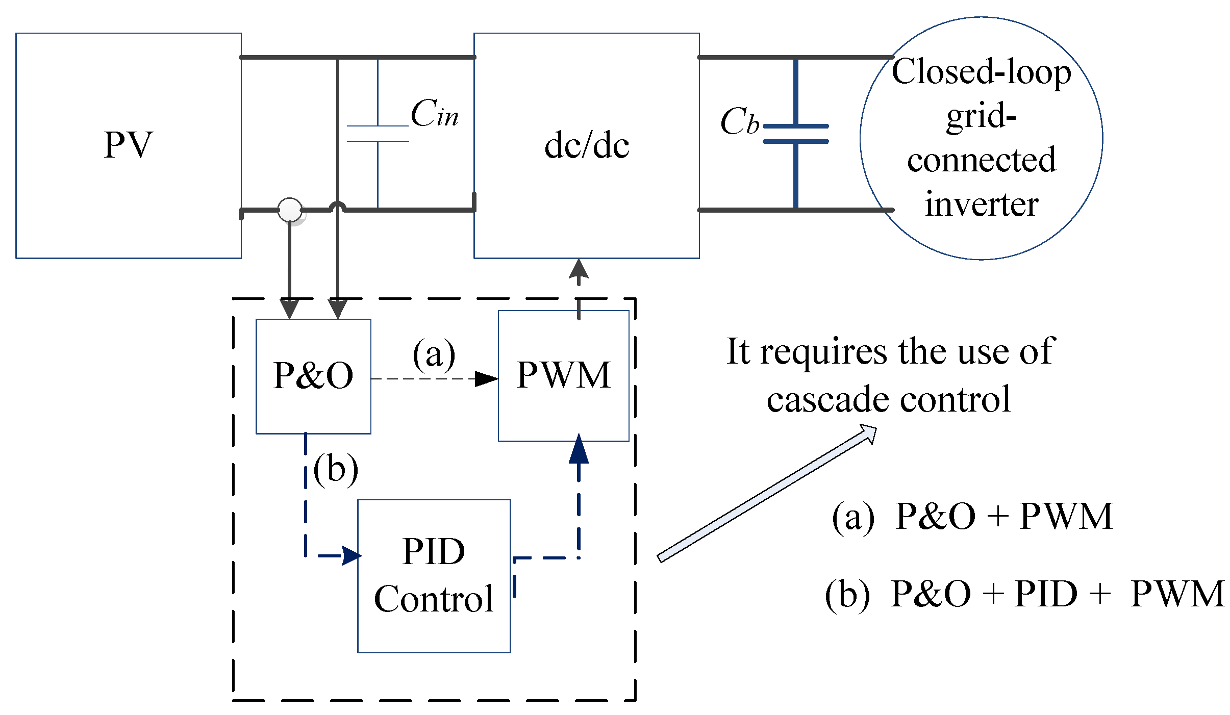
The structure of the two classical solutions based on the P & O algorithm are presented in
Figure 18: (a) a P & O algorithm defining the duty cycle of a PWM (P & O + PWM) driving the MOSFET; and (b) a P & O algorithm defining the voltage reference of a PID controller, which in turns defines the duty cycle of a PWM (P & O + PID + PWM). Such a figure put in evidence the advantages of the proposed solution: the SMC only requires a single control block, instead the classical solutions require two and three control blocks.
Figure 18.
Structure of a conventional Maximum Power Point Tracking (MPPT) architecture.
Figure 18.
Structure of a conventional Maximum Power Point Tracking (MPPT) architecture.
The P & O algorithms were designed following the guidelines given in [
3,
38], which are aimed to guarantee a perturbation period larger than the PV voltage settling time. Concerning the stand-alone P & O controller (a), the parameters are: perturbation period Ta = 0.5 ms and perturbation amplitude Δd = 0.2.
The design of the PID controller for the cascade P & O solution (b) was based on the system Equations (1)–(3) linearized at the lower irradiance condition (100 W/m
2) as suggested in [
3]. Then, the transfer function between the PV voltage and the duty cycle
is calculated as in Equation (45). It is important to remark that
changes with the solar irradiance and temperature, hence the settling time
ts of the PV voltage constantly changes [
39]:
Therefore, conventional linear controllers for PV systems must be designed at the longest settling time value, which is obtained for the larger value of
(lower irradiance, 100 W/m
2 in this example). Then, using the root-locus placement technique, the controller in Equation (46) was designed. The perturbation period of the P & O algorithm is designed for the worst case scenario (longest
) following the guidelines given in [
3], it leading to Ta = 0.5 ms and Δv
ref = 0.25 V (perturbation amplitude applied to the PID reference):
Finally, to provide a fair comparison, both P & O + PWM and P & O + PID + PWM were implemented with a switching frequency equal to 100 kHz, which is the same switching frequency exhibited by the SMC.
A first test was performed considering a much larger DC-link capacitance
to reduce the voltage oscillations generated by the inverter. This test also includes the start-up of the PV system and an irradiance perturbation at t = 0.65 s. The simulation results are presented in
Figure 19, where the fast tracking of the MPP provided by the proposed SMC is observed. The simulation also reports the small voltage oscillations exhibited due to the large value of
by the three systems, which enables the correct operation of the P & O + PWM solution. Finally, the fast response of the SMC is translated into a higher energy harvested from the PV array, which eventually increases the system profitability.
Figure 19.
Performance comparison between the SMC and conventional P & O-based solutions considering small DC-link voltage oscillations.
Figure 19.
Performance comparison between the SMC and conventional P & O-based solutions considering small DC-link voltage oscillations.
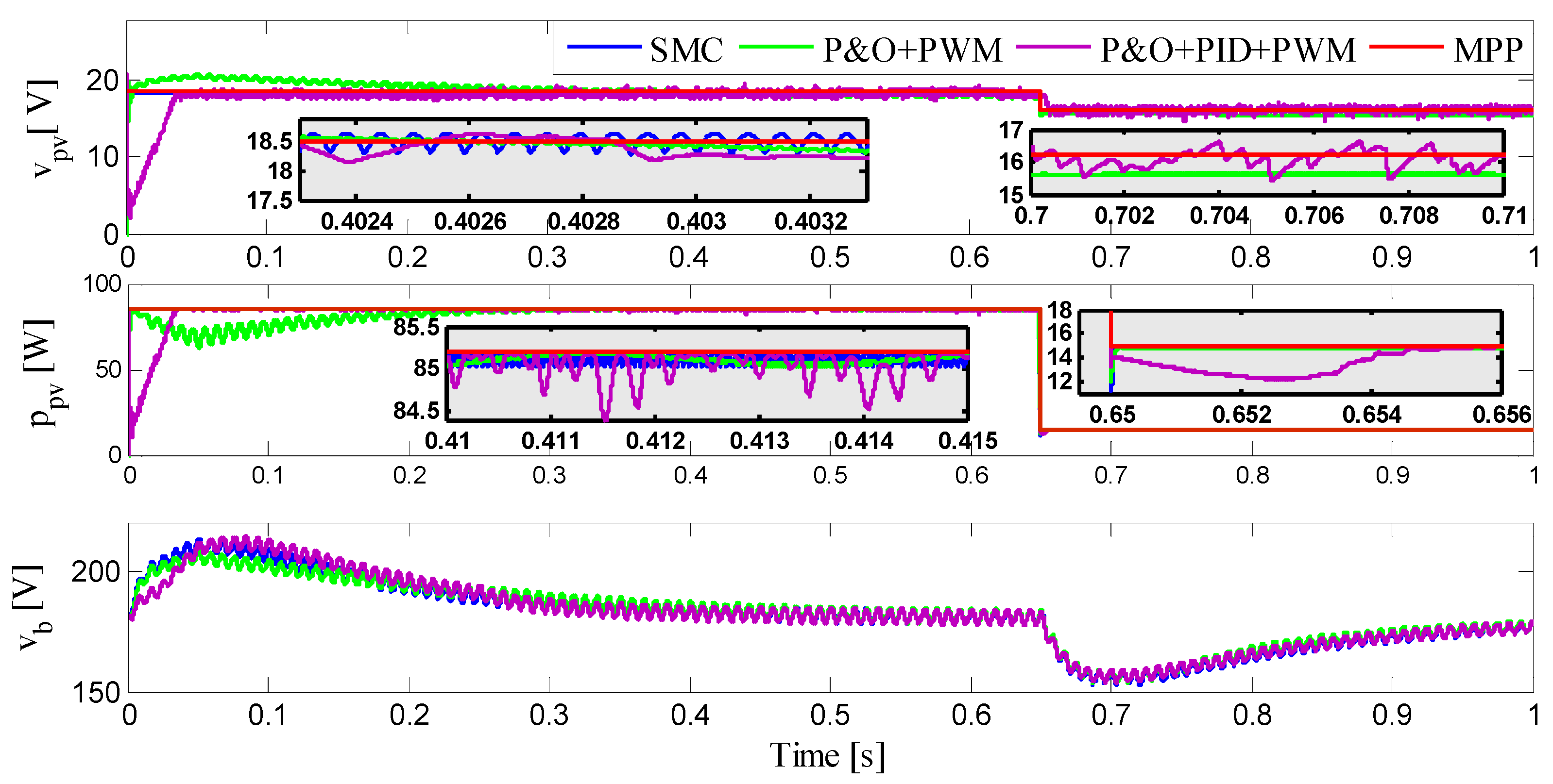
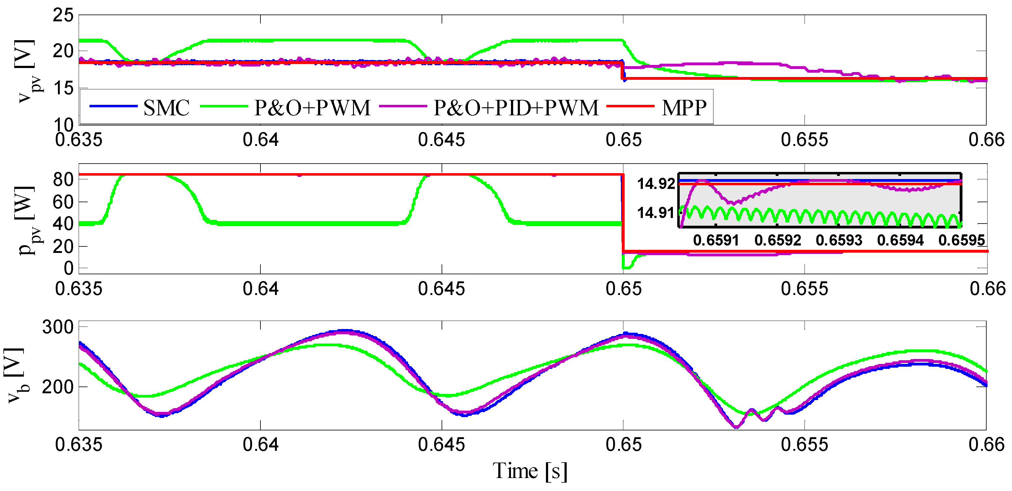
A second test was performed accounting for large voltage oscillations at the DC-link,
i.e., using a smaller
. The simulation results are reported in
Figure 20, where again the SMC exhibits a faster MPPT procedure with higher energy production. Moreover, the simplest P & O solution (P & O + PWM) is unstable since the DC-link voltage oscillations are transferred to the PV array terminals, which confuses the P & O algorithm. In contrast, the more complex P & O solution (P & O + PID + PWM) is stable, but it requires a long time to reach the MPP in comparison with the SMC.
Figure 20.
Performance comparison between the SMC and conventional P & O-based solutions considering large DC-link voltage oscillations.
Figure 20.
Performance comparison between the SMC and conventional P & O-based solutions considering large DC-link voltage oscillations.


