1. Introduction
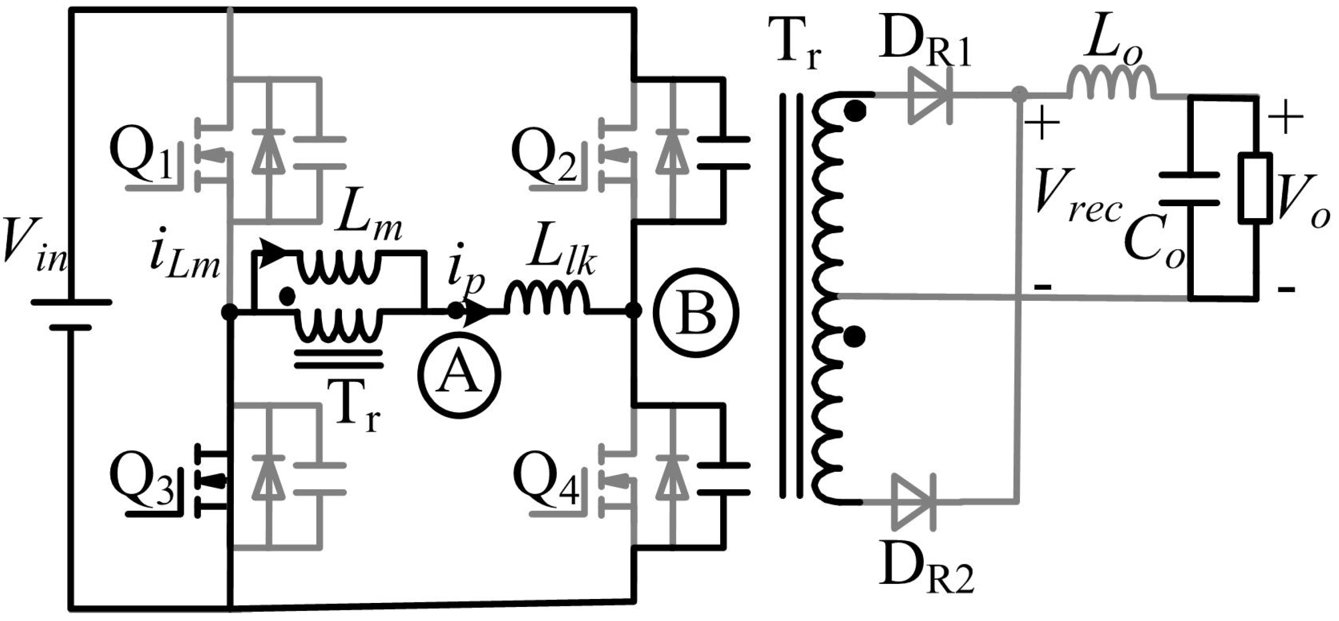
By using parasitic circuit elements such as junction capacitances of switches and leakage inductance of transformer, phase-shifted full-bridge (PSFB) converter provides zero-voltage-switching (ZVS) for switches without requiring any additional active devices [
1,
2]. These characteristics can reduce switching loss and enable high switching frequency operation. Such advantages make the PSFB converter well suited for high efficiency, high power density and high reliability applications [
3,
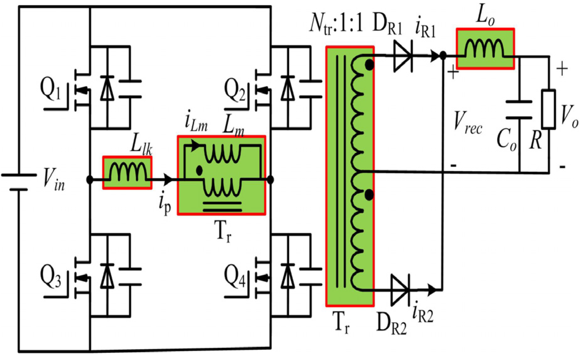
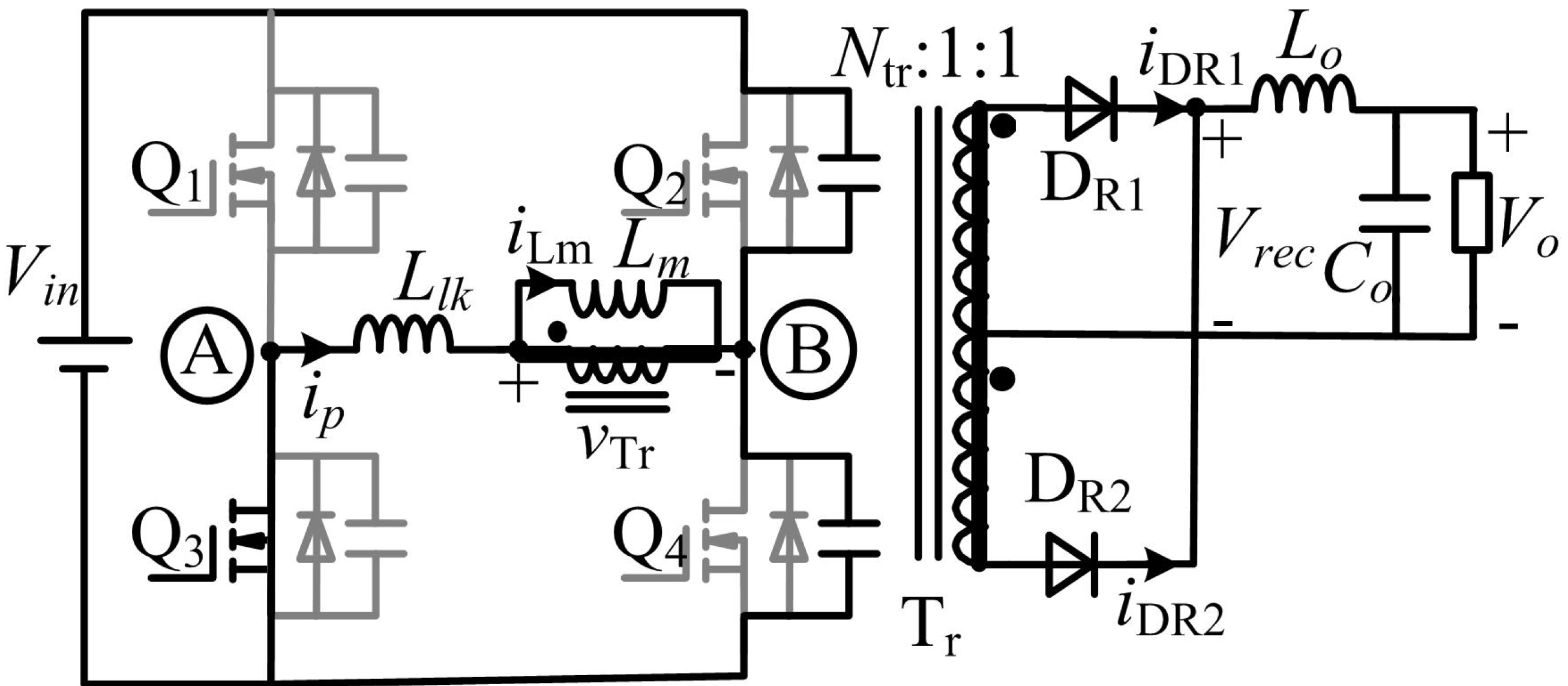
4]. The circuit diagram of a PSFB converter is shown in
Figure 1 [
5,
6]. T
r is the transformer which can be used as electric isolation and energy conversion.
Lm is the magnetizing inductance of T
r.
Llk is the resonant inductance which includes the leakage inductance of T
r and an external inductance added to extend the ZVS range.
Lo is the output filter inductance. As shown in
Figure 1, magnetic components are important parts of the converter and they determine the operation modes and size of the converter [
7,
8,
9].
Figure 1.
Circuit diagram of a phase-shifted full-bridge (PSFB) converter.
Figure 1.
Circuit diagram of a phase-shifted full-bridge (PSFB) converter.
The drawback of PSFB converter is the dependency of ZVS characteristic on load conditions. ZVS is lost at light loads since energies which are stored in magnetic components are insufficient to fully discharge the output capacitances of switches. The loss of ZVS results in high Electromagnetic Interference (EMI) and low efficiency due to the increase of switching loss. The methods proposed in [
10,
11,
12,
13] can extend the ZVS range by adding auxiliary circuits which provide enough energies to achieve complete ZVS for all switches. Several methods to improve the efficiency of PSFB converter have been proposed, especially under light load conditions, with no additional devices. By properly selecting magnetizing inductance and resonant inductor [
14], ZVS operation can be maintained in all capacity loads. The converter achieves high light-load efficiency with a penalty on the heavy-load efficiency. By adjusting switching control technique of full-bridge converter [
15], the efficiency improvement can be up to 20%. However, switches operate with hard switching. The methods shown in [
16,
17] can reduce switching loss by changing dead-time and thus the light load efficiency can be improved.
In order to avoid overshooting, dead-time is needed between switches located in the same leg. Dead-time is a key parameter that needs to be optimized during the converter design. In the conventional design procedure, dead-time is constant regardless of load conditions, which results in additional loss due to the switch body diode reverse recovery and conduction. During dead-time of the PSFB converter, ZVS operation is achieved by using the energies stored in magnetic components to discharge and charge the output capacitances of switches. Dead-time is usually calculated under a given set of pre-defined load conditions. As a result, the available energies are insufficient and ZVS capability is lost at light loads.
Standby power is electricity consumed by an appliance while it doesn’t perform its primary function. A typical family, often having 20 devices, constantly draws standby power which is responsible for 5%–10% of the total power loss. The International Energy Agency (IEA) has proposed the one-watt plan, and the participating countries seek to lower standby power loss to below 1 watt in all products. To minimize the power consumption of power supplies in standby mode, some techniques have been proposed in [
15].
In this paper, the detailed circuit analysis of PSFB converter during dead-time is performed. According to the analysis results, magnetic component and dead-time values have a great effect on the range of ZVS. Dead-time value needs to be varied with the load current so that the energies stored in magnetic components can be taken full advantage of. In order to ensure that the available energies are always greater than the required energies for ZVS operation over a wide range of loads, magnetic component values are chosen based on circuit analysis results during dead-time. Such choice procedure can extend the ZVS range and improve the light-load efficiency of PSFB converter. Moreover, the converter is controlled by burst mode under standby condition and the standby power loss is less than 1 watt.
This paper is organized as follows: a detailed circuit analysis during dead-time is presented in
Section 2.
Section 3 discusses the relationships between the available energies for ZVS and values of magnetic components. The proposed choice procedure of magnetic component values and control system are described in
Section 4. In
Section 5, experimental results are presented and discussed. The conclusions are given in
Section 6.
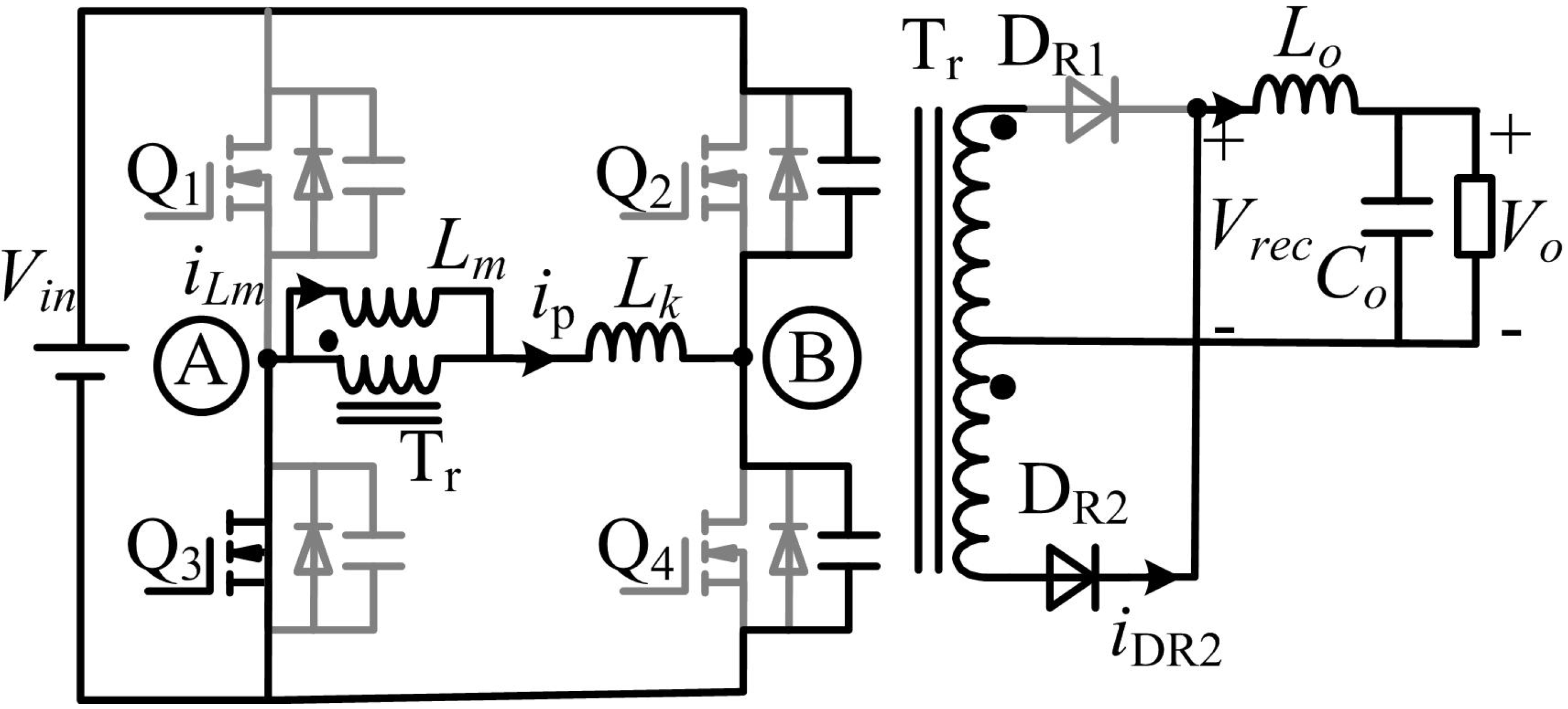
2. Circuit Analysis
As load current decreases, the current through the output filter inductor will be discontinuous. The operation principle of PSFB converter in discontinuous current mode (DCM) is different from that in continuous current mode (CCM). The operation principles of the PSFB converter have been discussed in [
5,
6].
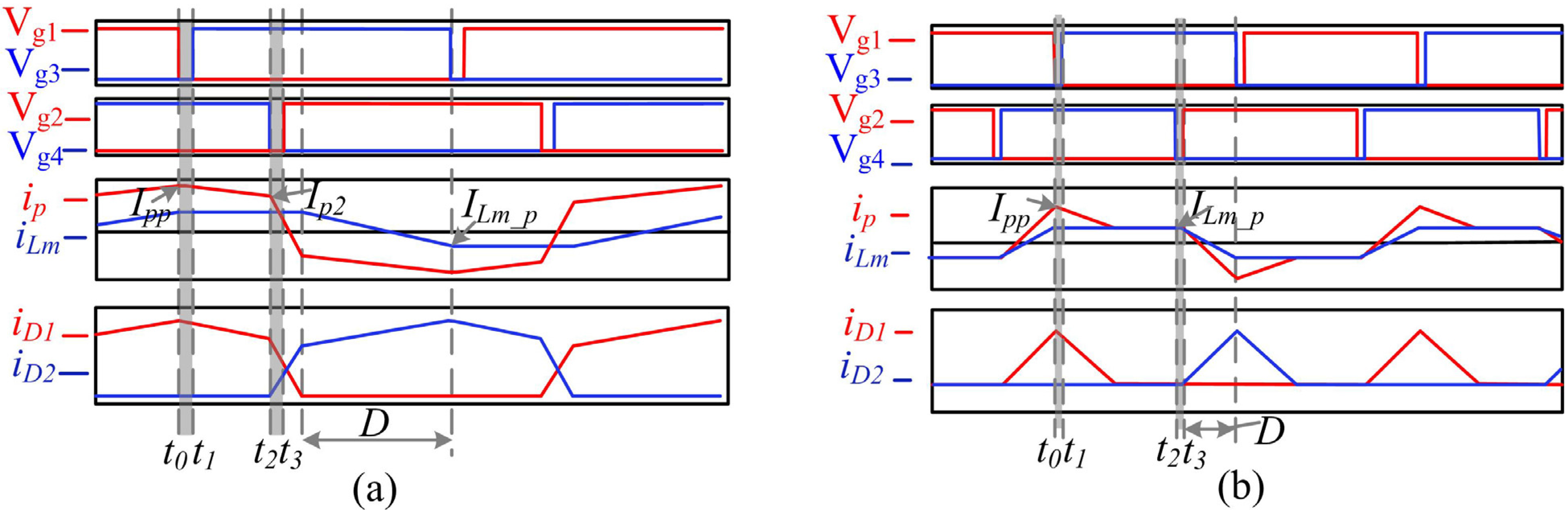
Figure 2 shows the steady waveforms in different modes and the key values can be calculated as follows.
Figure 2.
Key waveforms in different modes: (a) Continuous current mode (CCM); (b) Discontinuous current mode (DCM).
Figure 2.
Key waveforms in different modes: (a) Continuous current mode (CCM); (b) Discontinuous current mode (DCM).
The duty cycle of primary voltage which is set by the controller, can be expressed as:
The peak value of primary current
Ipp which corresponds to the output filter inductor current reflected to the primary side is described as:
where Δ
Iout is the current ripple of
Lo.
The peak value of magnetizing current is calculated as:
The primary current at
t2 in CCM operation is
In order to ensure ZVS and avoid overshooting, dead-time is needed between the switches located in the same leg. During dead-time, ZVS is achieved by using the energy stored in magnetic components to discharge and charge the output capacitances of switches. The detailed circuit analysis during dead-time is presented as follows.
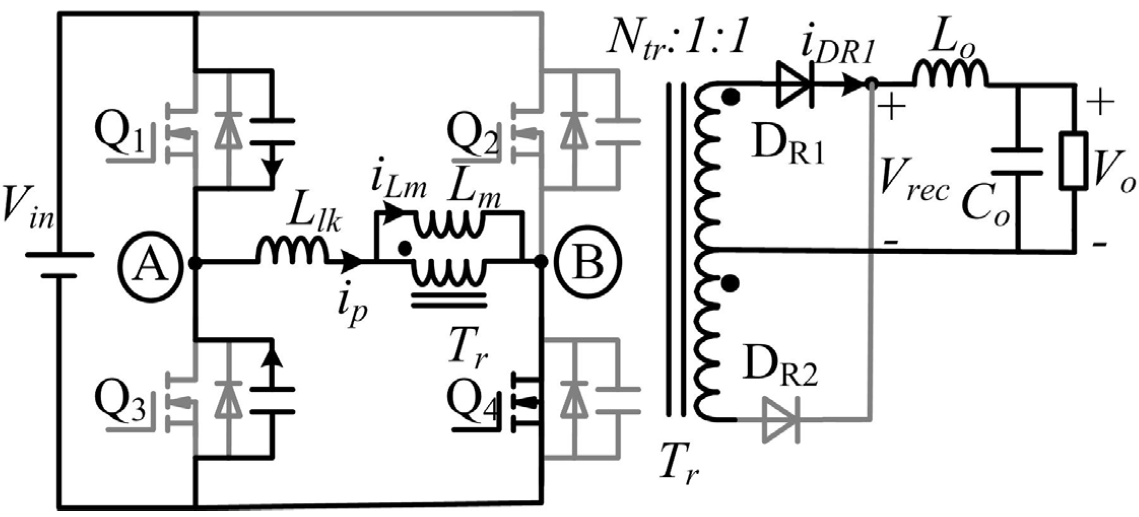
2.1. Circuit Analysis during the Dead-Time of Leading-Leg
Q
1 is turned off at
t0 and the primary current increases to
Ipp. The output capacitances of Q
1 and Q
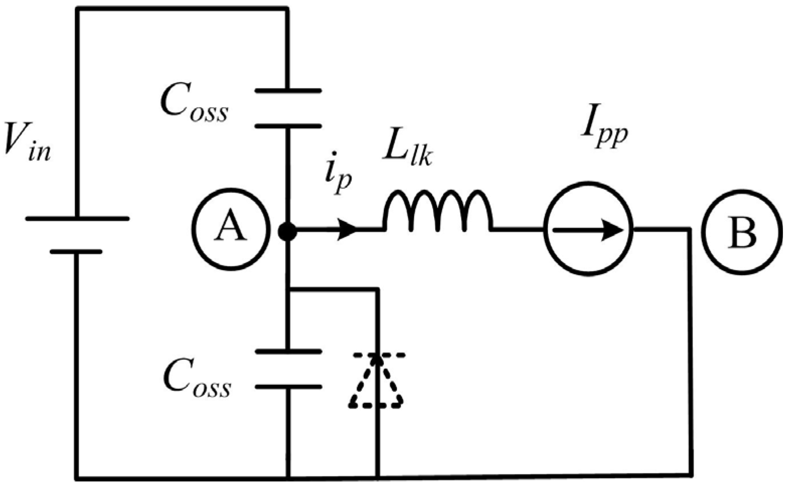
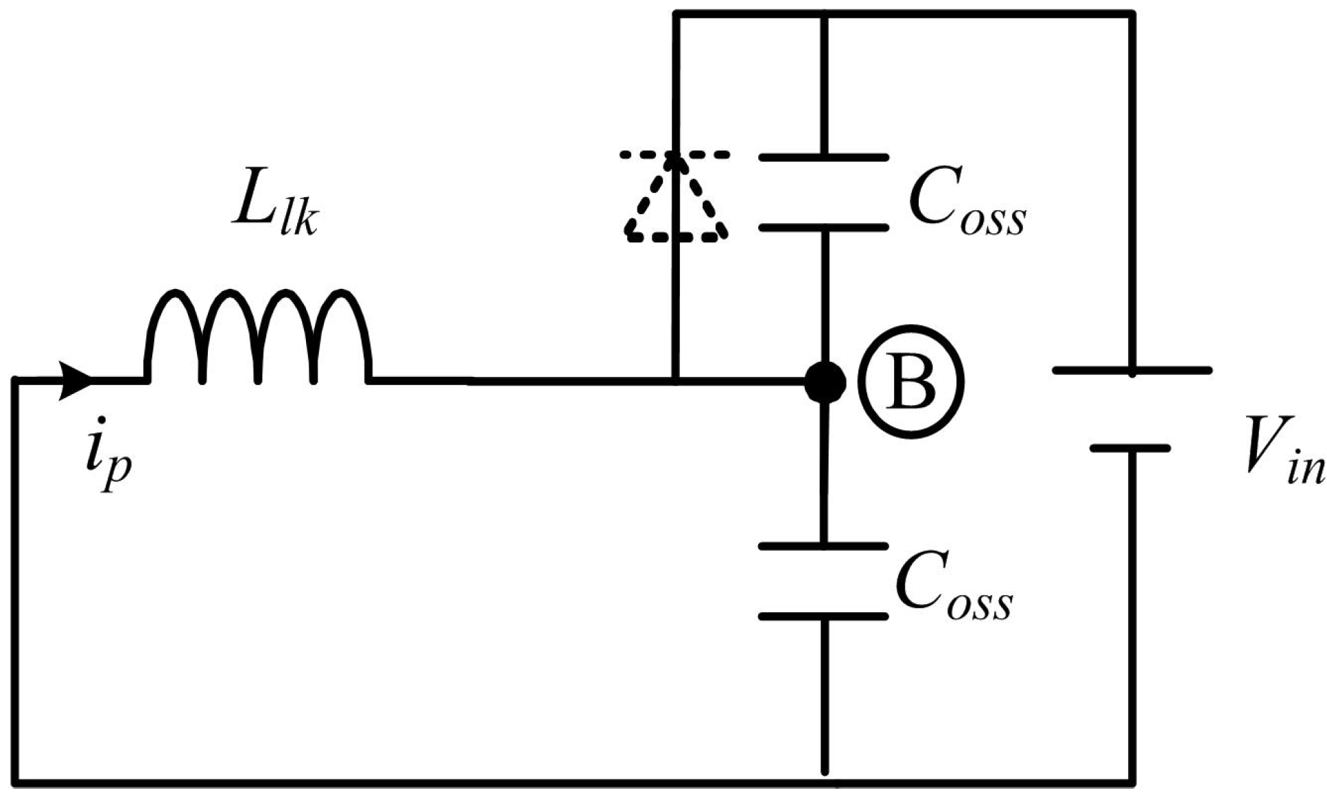
3 start to charge and discharge respectively. During the dead-time of leading-leg, the equivalent circuit of the converter in DCM operation is the same as that in CCM operation.
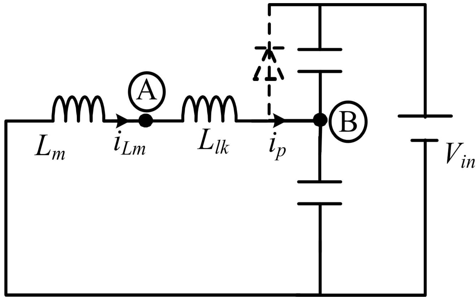
Figure 3 shows the equivalent circuit and this circuit can be simplified as
Figure 4. When the diode drawn with dashed line (the body diode of Q
3) comes into conduction in
Figure 4, the switch Q
3 can be turned on with ZVS. In this interval, the filter inductor is transformed to the primary side and the primary current is regarded as a constant current source.
Figure 3.
Equivalent circuit during [t0, t1].
Figure 3.
Equivalent circuit during [t0, t1].
Figure 4.
Simplified circuit during [t0, t1].
Figure 4.
Simplified circuit during [t0, t1].
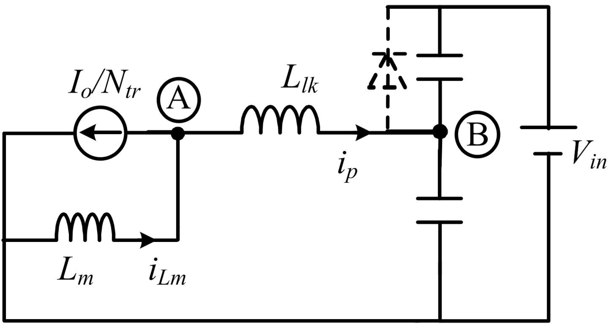
2.2. Circuit Analysis during the Dead-Time of Lagging-Leg
Q
4 is turned off at
t2 and the converter starts to operate under the dead-time of lagging-leg condition. In order to analyze the effect of dead-time, it is assumed that dead-time is very wide. At the beginning of this transition, the rectifier diodes conduct at the same time. The summed current of D
R1 and D
R2 is equal to load current, the current of D
R1 decreases while the current of D
R2 increases. When the body diode of Q
2 comes into conduction, the transition is over. Depending on the load condition, the following three cases are possible during the lagging-leg transition [
14]:
Case 1: The converter is in CCM operation and magnetizing current is smaller than the reflected load current. Resonance occurs between
Llk and output capacitances of Q
2 and Q
4. D
R1 and D
R2 conduct at the same time and thus the transformer is shorted.
Figure 5 shows the equivalent circuit which can be simplified as
Figure 6.
Figure 5.
Equivalent circuit in Case 1.
Figure 5.
Equivalent circuit in Case 1.
Figure 6.
Simplified circuit in Case 1.
Figure 6.
Simplified circuit in Case 1.
Case 2: The converter is in CCM operation and magnetizing current is larger than the reflected load current. The dead-time is wide while the converter still operates under the dead-time of lagging-leg condition. The transformer comes out of the shorted state and starts to transfer energy to the output side.
Figure 7 shows the equivalent circuit in Case 2 and it can be simplified as
Figure 8.
Figure 7.
Equivalent circuit in Case 2.
Figure 7.
Equivalent circuit in Case 2.
Figure 8.
Simplified circuit in Case 2.
Figure 8.
Simplified circuit in Case 2.
Case 3: The converter is in DCM operation. The current through
Lo is zero and the rectifier diodes are turned off.
Figure 9 shows the equivalent circuit in Case 3 and it can be simplified as
Figure 10. The available energies to charge and discharge the capacitances are mainly stored in the magnetizing inductance.
Figure 9.
Equivalent circuit in Case 3.
Figure 9.
Equivalent circuit in Case 3.
Figure 10.
Simplified circuit in Case 3.
Figure 10.
Simplified circuit in Case 3.
3. Available Energies for Zero-Voltage-Switching (ZVS) operation
The switch can achieve the ZVS operation during dead-time intervals by using the energies stored in magnetic components to force conduction of the switch’s bode diode before turning the switch on. The available energies are related to the load condition which results in the ZVS characteristic loss at light loads.
As shown in
Figure 4, the filter inductor is transformed to the primary side and the primary current is regarded as a constant current source to charge and discharge the output capacitances during the dead-time of leading-leg. The leading-leg switches can be turned on with ZVS easily. The required dead-time for leading-leg can be expressed as:
where
Coss is the output capacitance of the Metal-Oxide-Semiconductor-Field-Effect Transistor (MOSFET).
However, the lagging-leg switches are difficult to obtain ZVS operation since the filter inductor doesn’t participate in the transition. According to the circuit analysis during the dead-time of lagging-leg, the required energy
Ereq for completely charging and discharging the capacitances can be expressed as:
As shown in
Figure 6, only the energy stored in
Llk takes part in ZVS transition when the converter operates in Case 1 since the transformer is shorted. The available energy
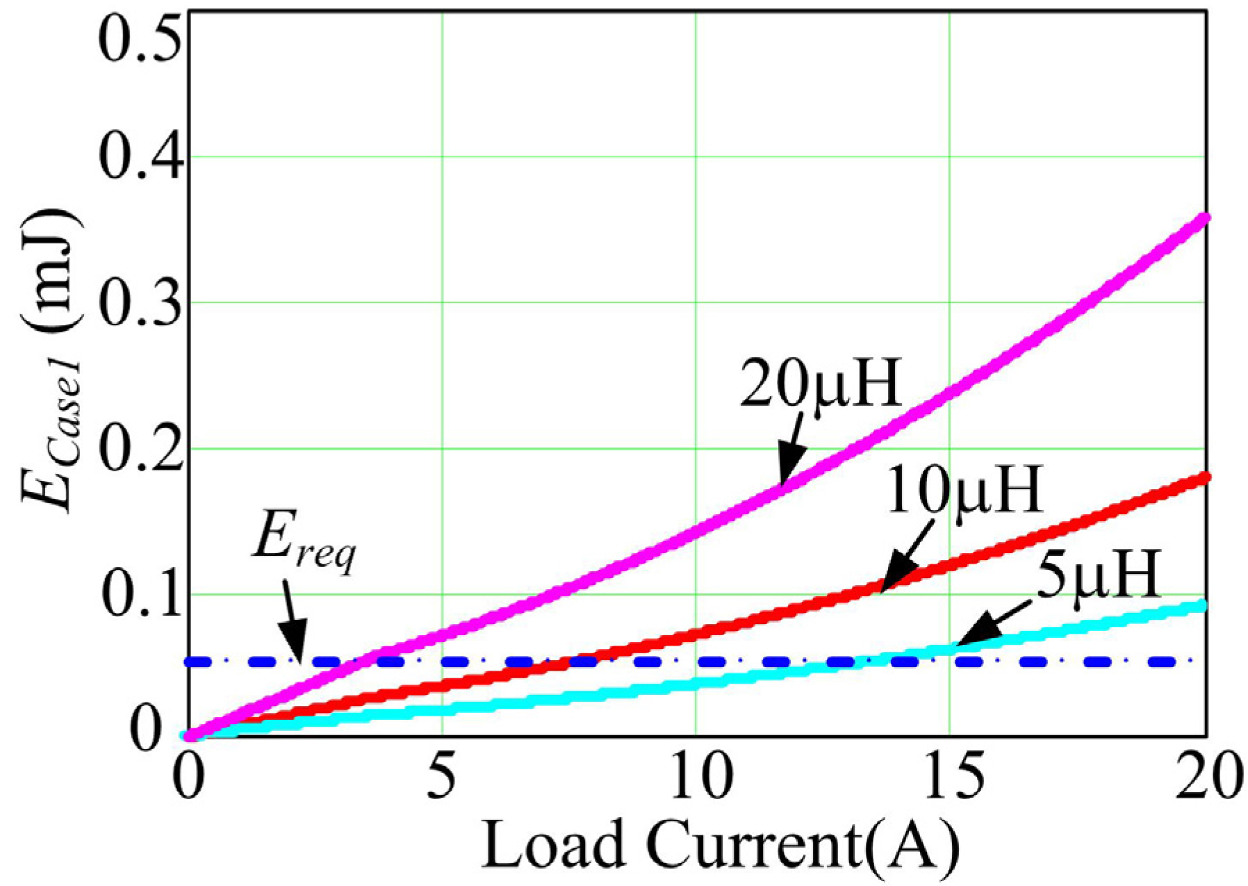
ECase1 can be expressed as follows:
Figure 11 shows the available energy with various resonant inductances
vs. load current. To realize ZVS operation, the available energy
ECase1 should be larger than the required energy
Ereq. The condition can be expressed as:
Figure 11.
Available energy in Case 1 vs. load current.
Figure 11.
Available energy in Case 1 vs. load current.
As shown in
Figure 11, the available energy increases with the value of
Llk. The ZVS range can be extended by using large resonant inductance. However, large resonant inductor reduces the effective duty cycle and increases both the conduction loss and voltage stress of the rectifier diodes. These disadvantages result in efficiency decay. The resonance between
Llk and
Coss provides a sinusoidal voltage across the switches. To ensure that all the energy stored in
Llk is available, the dead-time of lagging-leg
tLag is set one fourth of the resonant period as follows:
At the beginning of lagging-lag dead-time, the transformer is shorted and the converter operates in Case 1. Only when the load current satisfies the following condition can Case 2 exist:
When the current of D
R1 reaches zero, the converter operates in Case 2. From the simplified equivalent circuit of
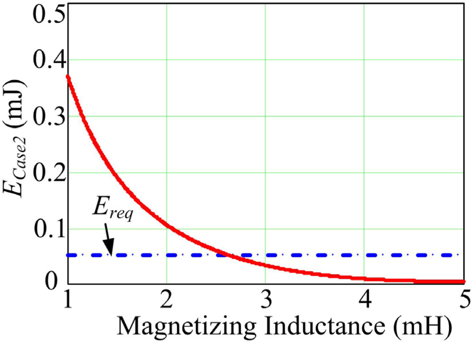
Figure 8, the energy stored in the magnetizing inductance can be used to provide ZVS and the available energy in Case 2 is:
Figure 12 shows the available energy
vs. magnetizing inductance. Small magnetizing inductance results in large magnetizing current, therefore
ECase2 increases while magnetizing inductance decreases. Dead-time should be enlarged since the magnetizing current is small and more time is needed to completely charge and discharge the capacitances.
ECase2 should be larger than the required energy
Ereq. The condition for ZVS operation in Case 2 can be expressed as:
When the load current is smaller than Δ
Iout, the converter enters in DCM operation. The critical load current between CCM and DCM can be calculated as follows:
As shown in
Figure 10, both
Llk and
Lm take part in ZVS transition in Case 3. Since
Llk is much smaller than
Lm, the available energy in Case 3 is mainly stored in
Lm, which is given by Equation (14).
Figure 12.
Available energy in Case 2 vs. magnetizing inductance.
Figure 12.
Available energy in Case 2 vs. magnetizing inductance.
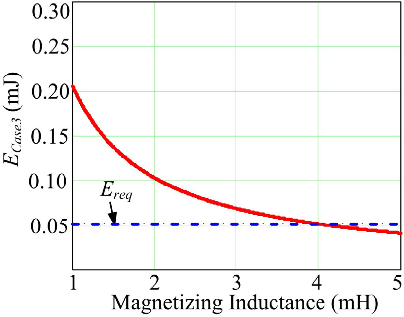
Figure 13 shows the available energy in Case 3
vs. magnetizing inductance. The condition for ZVS operation in Case 3 can be expressed as:
During dead-time in Case 3, the resonance between the magnetizing inductance and capacitances provides a sinusoidal voltage across the switches. The dead-time is set at one fourth of the resonant period.
Figure 13.
Available energy in Case 3 vs. magnetizing inductance.
Figure 13.
Available energy in Case 3 vs. magnetizing inductance.
4. Proposed Choice Procedure and Control Method
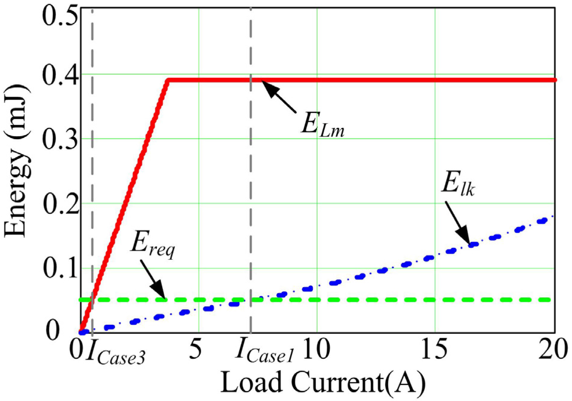
The PSFB converter can use the energies stored in magnetic components to discharge junction capacitances during dead-time and thus the switches can achieve ZVS.
Figure 14 shows the stored energies and required energy for ZVS operation
vs. load current. The drawback of PSFB converter is the dependency of ZVS characteristic on load condition. If the converter is controlled by the conventional fixed dead-time method, only Case 1 exists during the lagging-leg dead-time. The available energy is stored in the resonant inductance while the magnetizing inductance doesn’t take part in the ZVS transition. Only when the load current is greater than
ICase1, can the lagging-lag switches achieve ZVS operation. By carefully choosing magnetizing component values and adopting variable dead-time method, the energy stored in the magnetizing inductance can be used to provide ZVS transition energy and the ZVS range can be extended from
ICase1 to
ICase3.
Figure 14.
Stored energies and required energy vs. load current.
Figure 14.
Stored energies and required energy vs. load current.
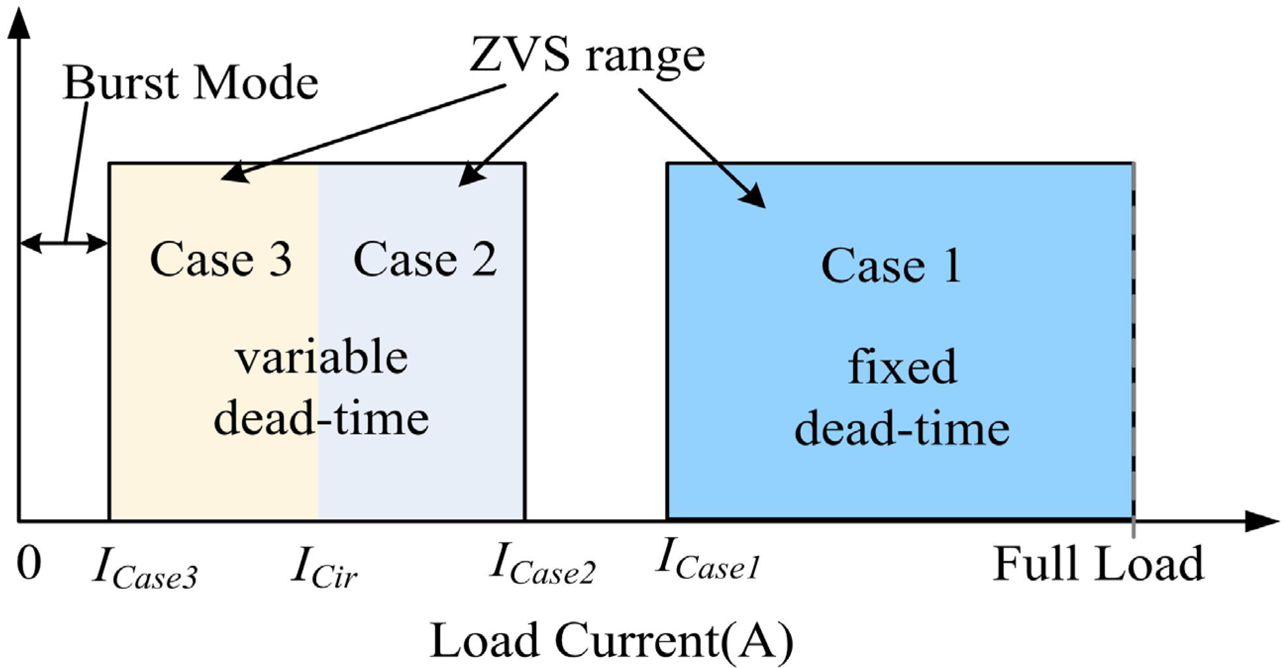
Three cases are possible during the dead-time of lagging-lag, as shown in
Figure 15. By adopting the variable dead-time control method, the lagging-leg switches can achieve ZVS operation when load current locates in the colorful areas. If
ICase2 is greater than
ICase1, the ZVS range of lagging-leg can be extended to
ICase3. According to Equations (8) and (12), the condition can be expressed as:
Lo can reduce output voltage ripple and its value is usually calculated as follows:
Figure 15.
Operational modes with the variable dead-time control.
Figure 15.
Operational modes with the variable dead-time control.
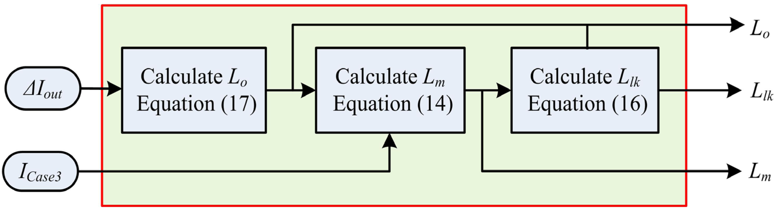
Figure 16 shows the proposed choice procedure of magnetic component values. Δ
Iout is the current ripple of
Lo and
ICase3 is the minimum load current for ZVS operation, which are usually given by the converter designer. In general, Δ
Iout is set at 20 percent of full load current and
ICase3 is set at 1~3 percent.
Figure 16.
Block diagram of the proposed choice procedure.
Figure 16.
Block diagram of the proposed choice procedure.
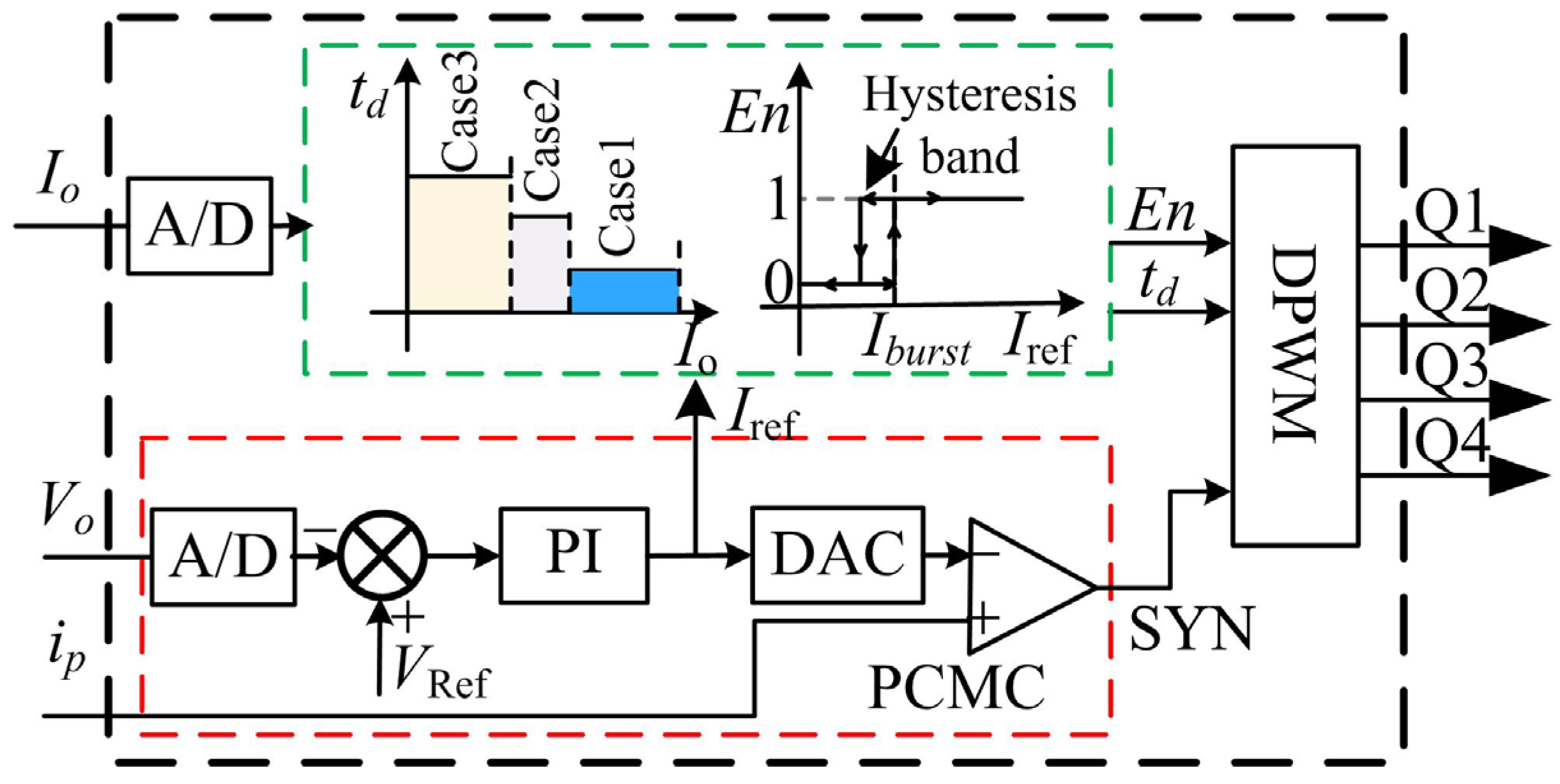
Figure 17 shows the block diagram of the proposed control method. The control system consists of two individual control loops. The first loop regulates the output voltage by controlling the phase-shift angle. In order to balance the flux of transformer and improve dynamic response, peak current mode control (PCMC) is adopted. The proportional integral (PI) controller determines the peak current reference signal
Iref. Primary current
ip is compared with
Iref and then the output synchronizing signal (SYN) of the on-chip analog comparator determines the phase-shift angle. The second loop adjusts dead-time
td and pulse width modulation (PWM) signals. According to the load current
Io, the controller adjusts
td according to the following rules:
- (1)
Under heavy loads (in Case 1), the available energies stored in Llk is sufficient to provide ZVS for lagging-lag switches and td is equal to 300 ns.
- (2)
When the load current locates in Case 2, the energy stored in magnetizing inductance can be used to charge and discharge capacitances by increasing td.
- (3)
Under light loads (in Case 3), the converter enters into DCM. td is set at one fourth of the resonant period between magnetizing inductance and capacitances.
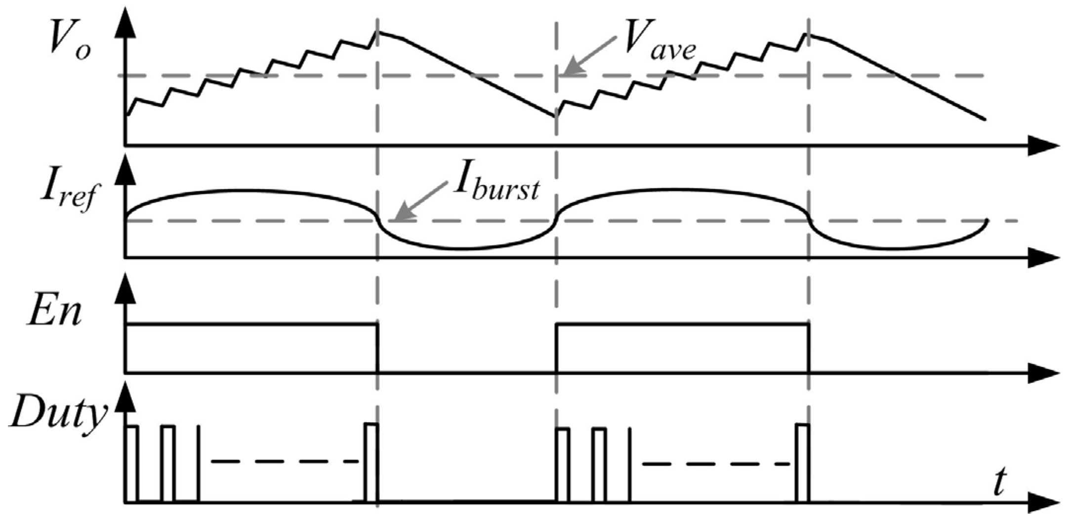
The converter enters into standby mode when the load current is less than
ICase3. In order to prevent bouncing between two switching modes, a hysteresis band is added.
Iburst is the peak primary current when load current is
ICase3. When primary current beyond
Iburst,
En = 1, and the PWM module enables output. In contrast,
En = 0, and the switching stops.
Figure 18 shows the key waveforms with burst mode control.
Vave is the average output voltage under standby condition.
Figure 17.
Control block diagram of the proposed method.
Figure 17.
Control block diagram of the proposed method.
Figure 18.
Key waveforms with burst mode control.
Figure 18.
Key waveforms with burst mode control.
5. Experimental Results
A 1-kW prototype is implemented to verify the advantages of the proposed method. The Digital-Signal-Processing (DSP) TMS320F28027 (Texas Instruments, Dallas, TX, USA) is adopted for the digital control of the PSFB converter. Considering the performance of DSP and influence of limit-cycle, the switching frequency is selected as 50 kHz. The input voltage
Vin is 400 V while the output voltage is 48 V. The turn ratio of transformer is 5:1:1, and rectifier diodes are STTH6002C. STW20NM60N is used as the primary switches and switching delay is 150 ns. The current ripple of
Lo, Δ
Iout, is 4 A and the minimum load current for ZVS operation,
ICase3, is 0.3 A. Based on the analysis of equations and the other specified parameters, the values of magnetic components and dead-time of lagging-leg are obtained.
Table 1 shows the calculation results.
Table 1.
Calculation results based on the proposed method.
Table 1.
Calculation results based on the proposed method.
| Calculation Results | Magnetic Components | Dead-Time of Lagging-Leg |
|---|
| Symbol | Lo | Lm | Llk | Case 1 | Case 2 | Case 3 |
| Value | 25 μH | 1.5 mH | 30 μH | 300 ns | 700 ns | 1.2 μs |
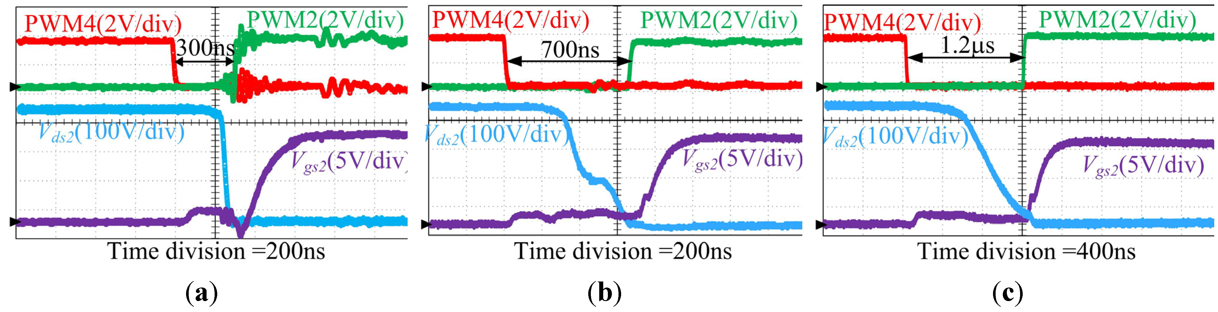
Figure 19 shows the waveforms of driver signals and voltage across Q
2 under different load conditions. By adopting the proposed choice procedure of magnetic component values, the lagging-lag switches are turned on with ZVS in all cases. The experimental results coincide with the theoretical analysis. The light-load efficiency of the converter with the proposed variable dead-time control method can be significantly improved since switching loss is dominant in Cases 2 and 3 operations.
Figure 19.
Experimental waveforms of Q2 under different load conditions. (a) Case 1, Io = 20 A; (b) Case 2, Io = 5 A; (c) Case 3, Io = 0.5 A.
Figure 19.
Experimental waveforms of Q2 under different load conditions. (a) Case 1, Io = 20 A; (b) Case 2, Io = 5 A; (c) Case 3, Io = 0.5 A.
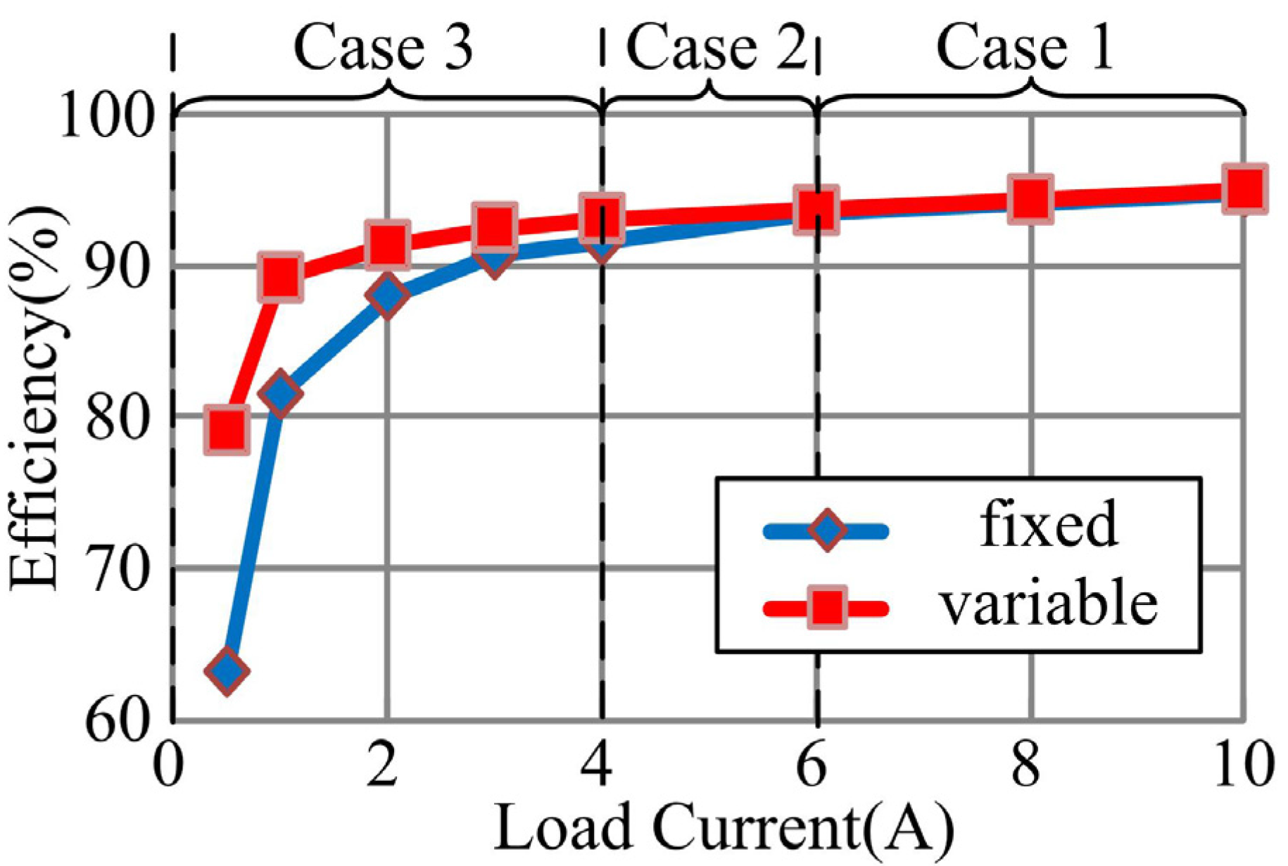
Figure 20 shows the measured efficiencies with the variable and fixed dead-time methods. It is clearly visible that the light-load efficiency is significantly improved since all switches can achieve ZVS operation.
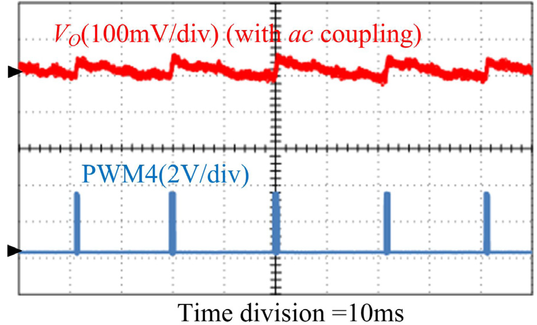
Figure 21 shows the key waveforms under standby condition. The proposed control method provides lower output voltage ripple as compared to the method shown in [
15]. As shown in
Figure 21, the equivalent switching frequency is significantly reduced by adopting burst mode. The standby power is 0.75 W and experiment result satisfies the requirement of “1 W plan”.
Figure 20.
Measured efficiencies with different control methods.
Figure 20.
Measured efficiencies with different control methods.
Figure 21.
Key waveforms under standby condition.
Figure 21.
Key waveforms under standby condition.


