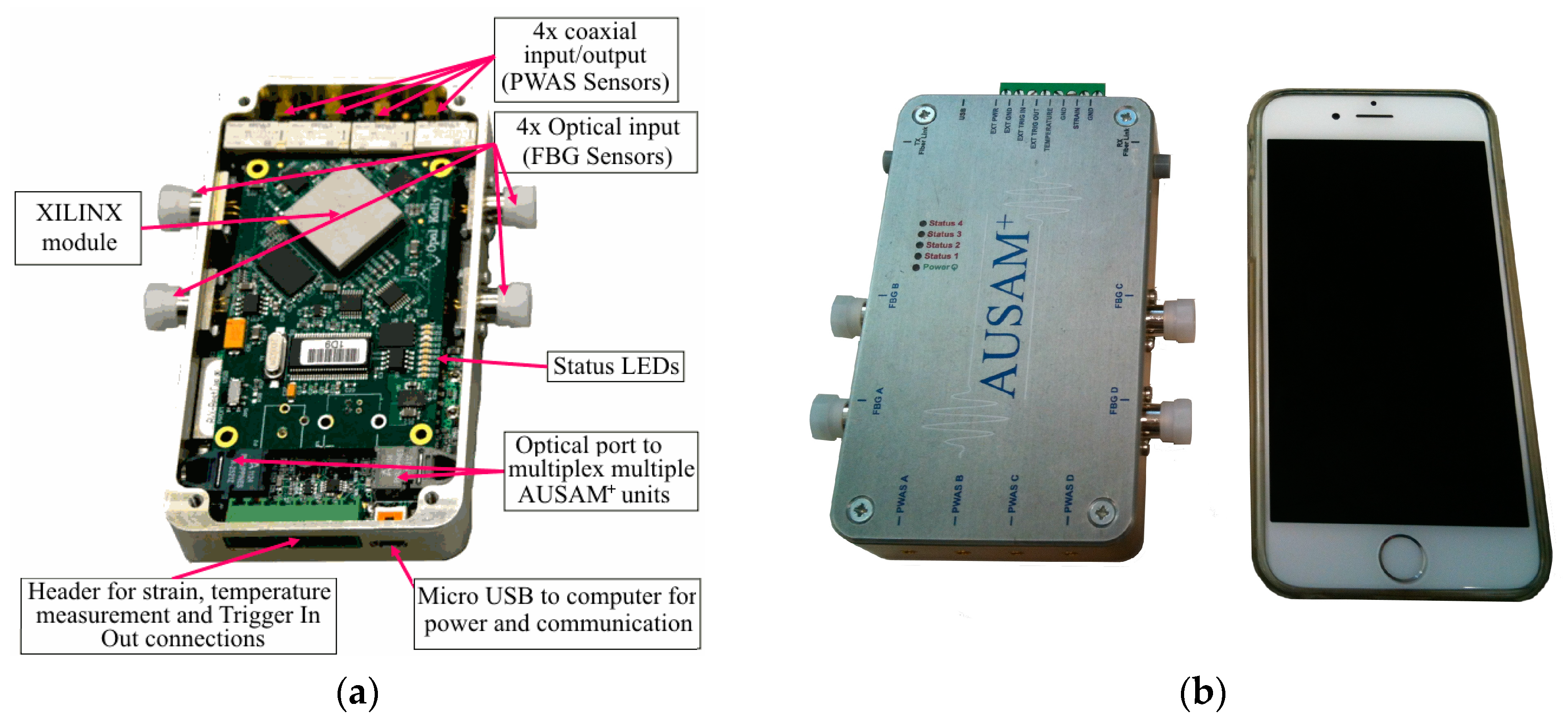
Figure 1.
Acousto Ultrasonic Structural health monitoring Array Module+ (AUSAM+) system: (a) Inputs and Outputs; (b) Size comparison to an iPhone 6.
Figure 1.
Acousto Ultrasonic Structural health monitoring Array Module+ (AUSAM+) system: (a) Inputs and Outputs; (b) Size comparison to an iPhone 6.
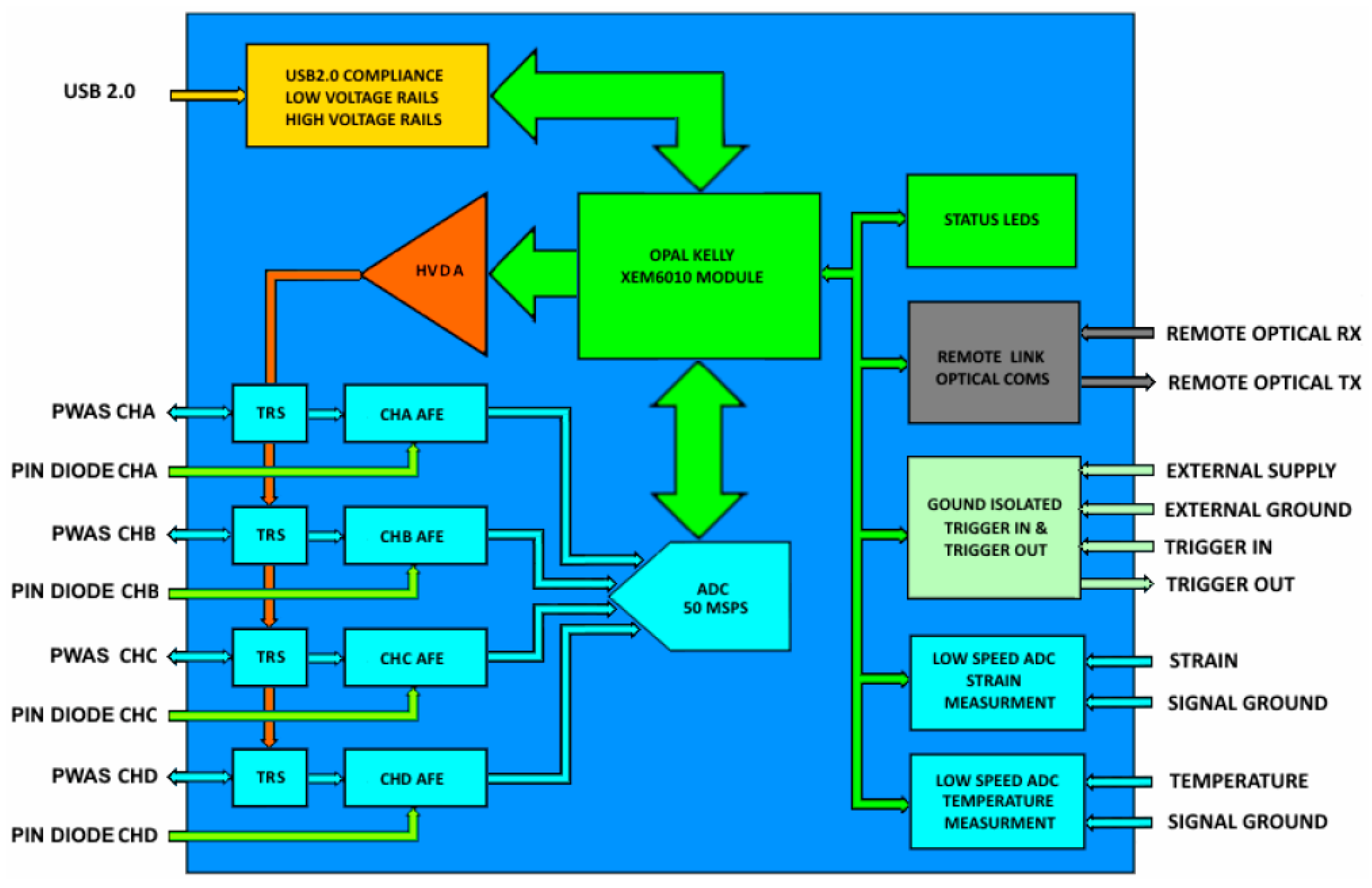
Figure 2.
AUSAM+ simplified block diagram.
Figure 2.
AUSAM+ simplified block diagram.
Figure 3.
Industrial Fiber Communication Ring for channel expansion and scalability. Up to 62 AUSAM+ can exist on the Industrial Fiber Communications Ring (IFCR).
Figure 3.
Industrial Fiber Communication Ring for channel expansion and scalability. Up to 62 AUSAM+ can exist on the Industrial Fiber Communications Ring (IFCR).
Figure 4.
AUSAM+ simplified Analogue Front End (AFE) channel architecture, where the four available channels are referenced A through D. The Drive Voltage Monitoring on/off switch and 1 MΩ divider resistor only exists on channel A and channel D while the Buffer Current Amplifiers, of which there are only two, have their outputs connected to channel B and channel C only.
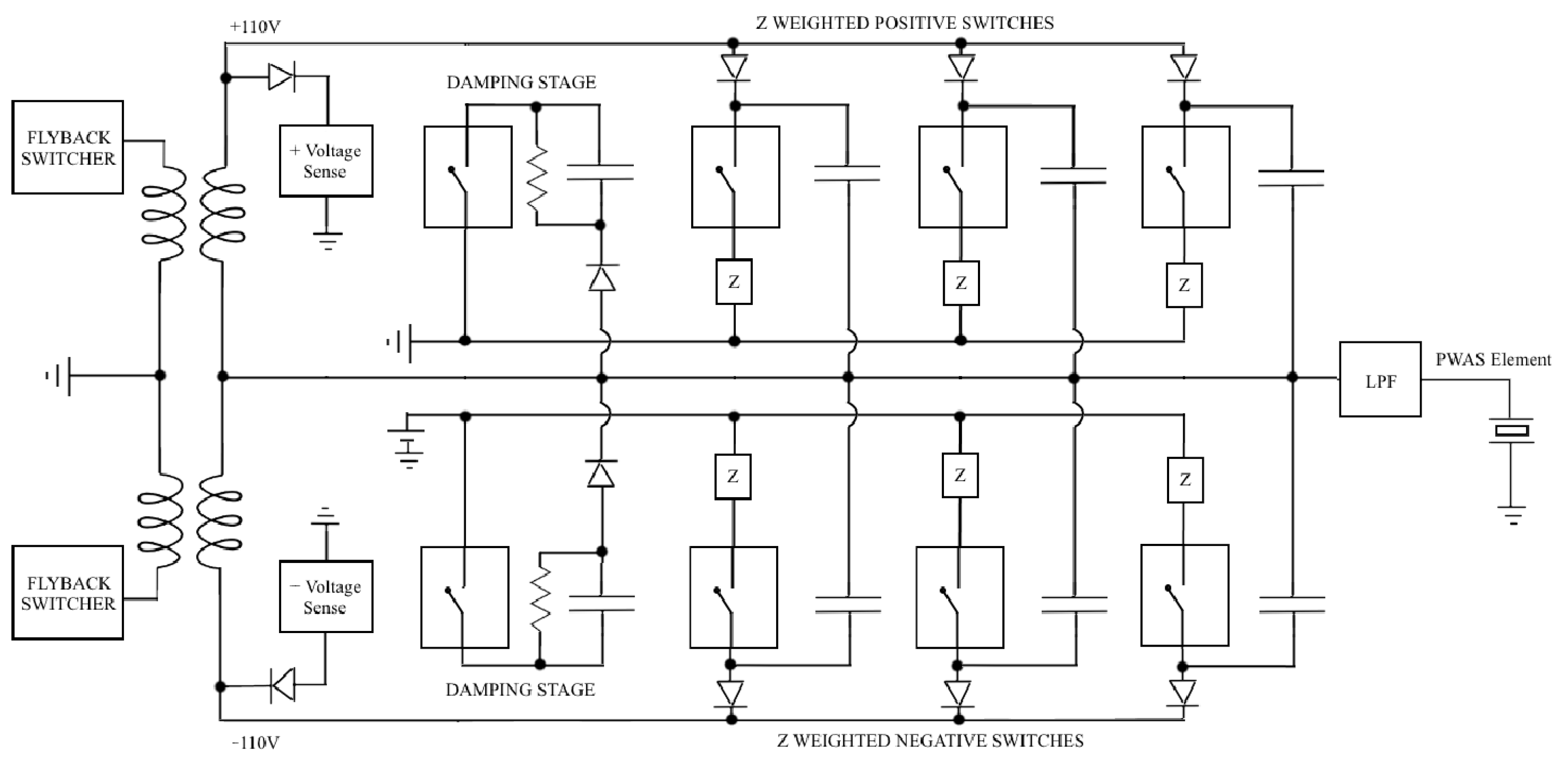
Figure 5.
AUSAM+ simplified High Voltage Drive Amplifier (HVDA) (not all swich elements shown).
Figure 5.
AUSAM+ simplified High Voltage Drive Amplifier (HVDA) (not all swich elements shown).
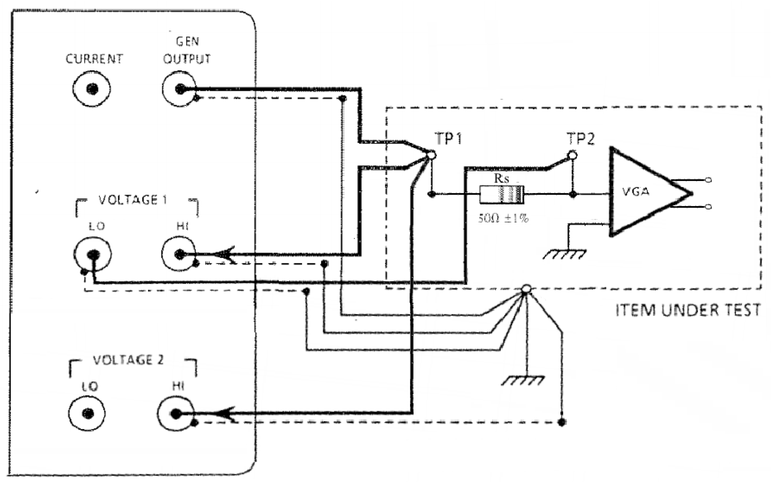
Figure 6.
Solatron 1260 measurement of the Variable Gain Amplifier (VGA) input impedance when the AFE channel is configured to monitor PWAS excitation voltage in Drive Monitor mode. The impedance between TP1 and ground is. The impedance between TP2, which is located at the AFE channels summing junction, and circuit ground, is the VGA input impedance.
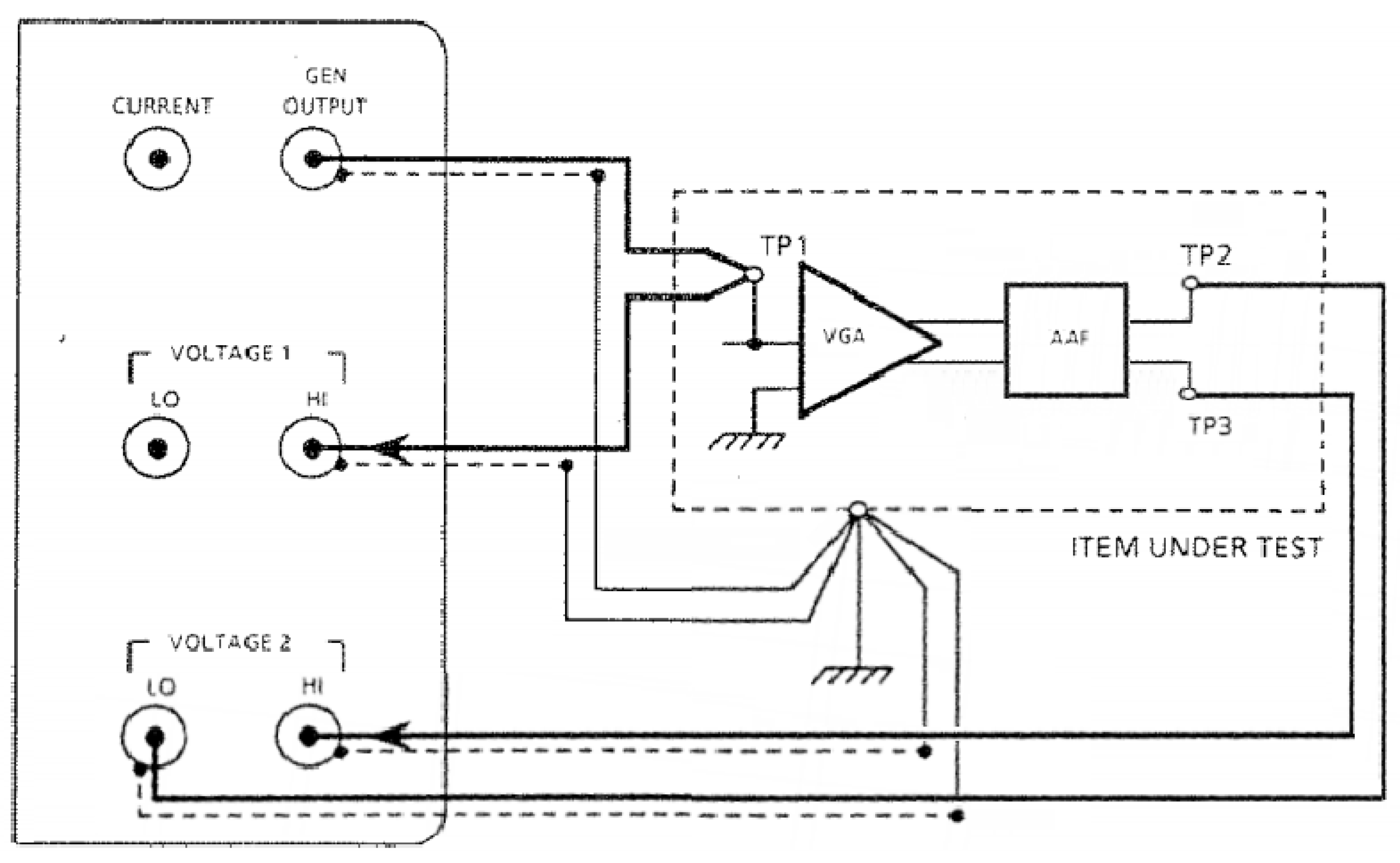
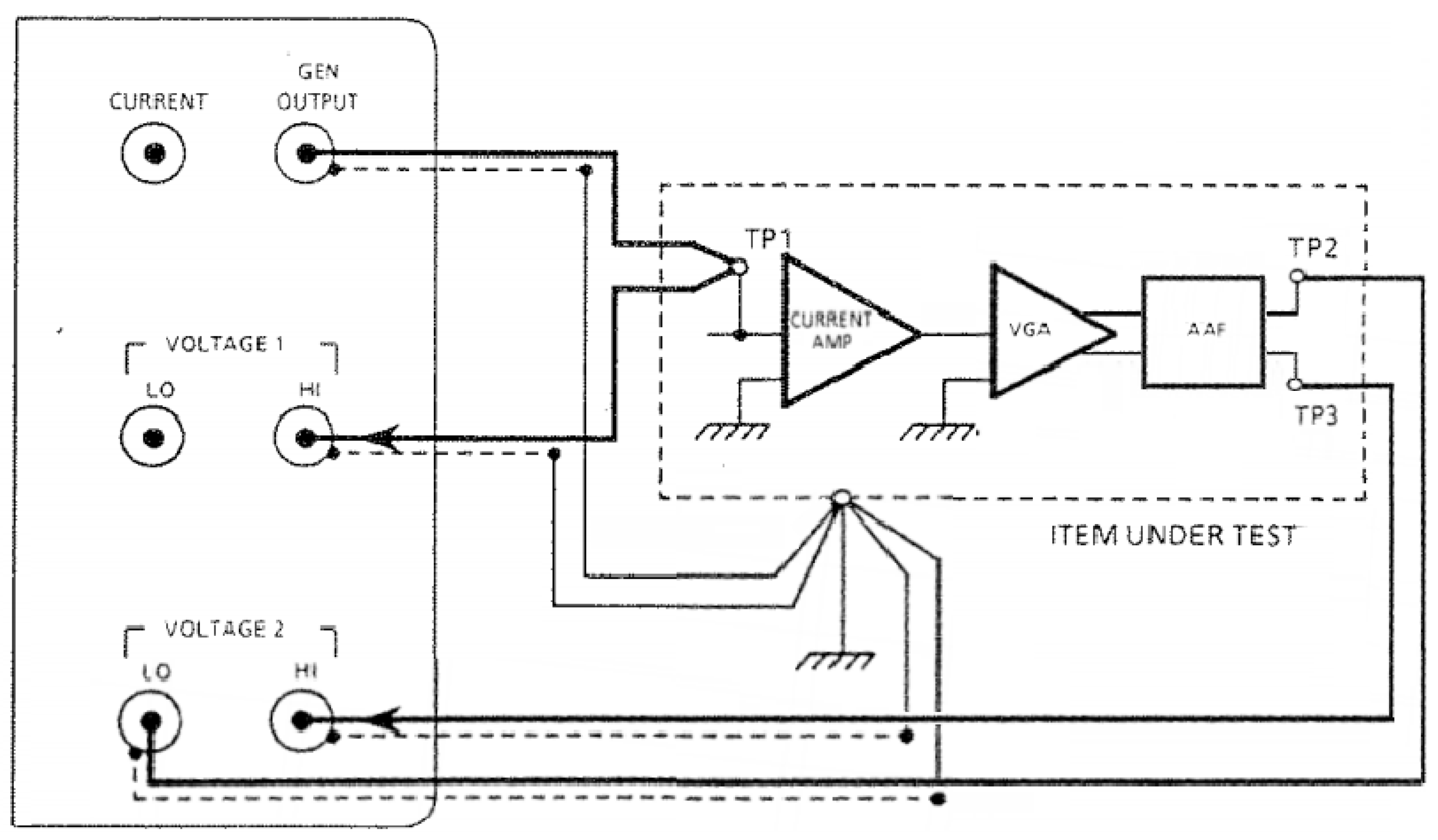
Figure 7.
Solatron 1260 measurement of the transfer functions (TF) as the measured Piezoelectric Wafer Active Sensor (PWAS) excitation voltage signal propagates through the remaining AFE channel when configured in Drive Monitor mode. TP1 is located at the AFE channels summing junction while TP2 and TP3 comprise the differential signal subsequently digitized by the high-speed Analog to Digital Converter (ADC).
Figure 8.
Solatron 1260 measurement of the TF as the measured PWAS excitation current signal propagates through the AFE channel when configured in Drive Monitor mode. TP1 correlates to the input of the current amplifier while TP2 and TP3 comprise the differential signal subsequently digitized by the high-speed ADC.
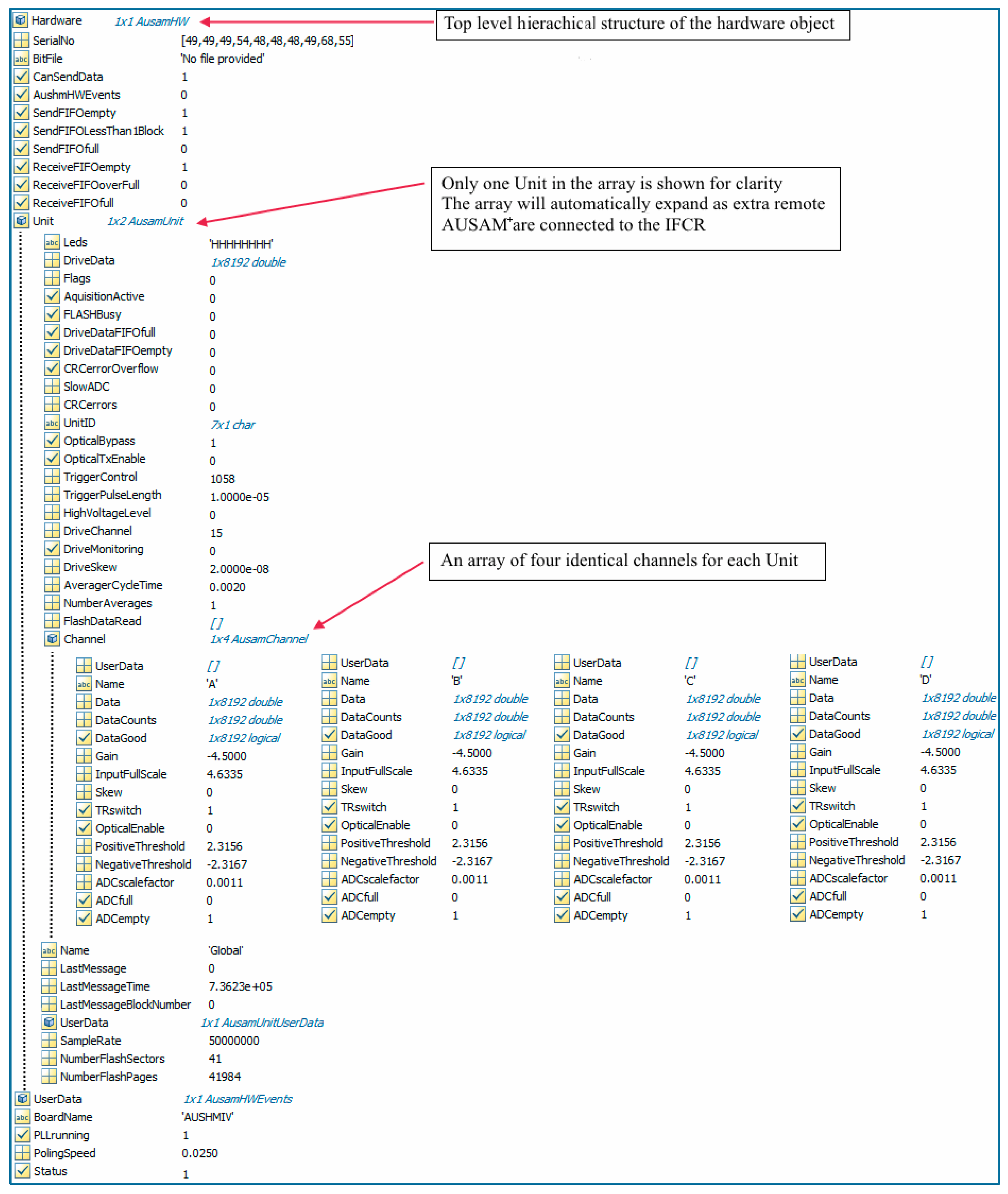
Figure 9.
AUSAM+ hardware object hierarchy and contents.
Figure 9.
AUSAM+ hardware object hierarchy and contents.
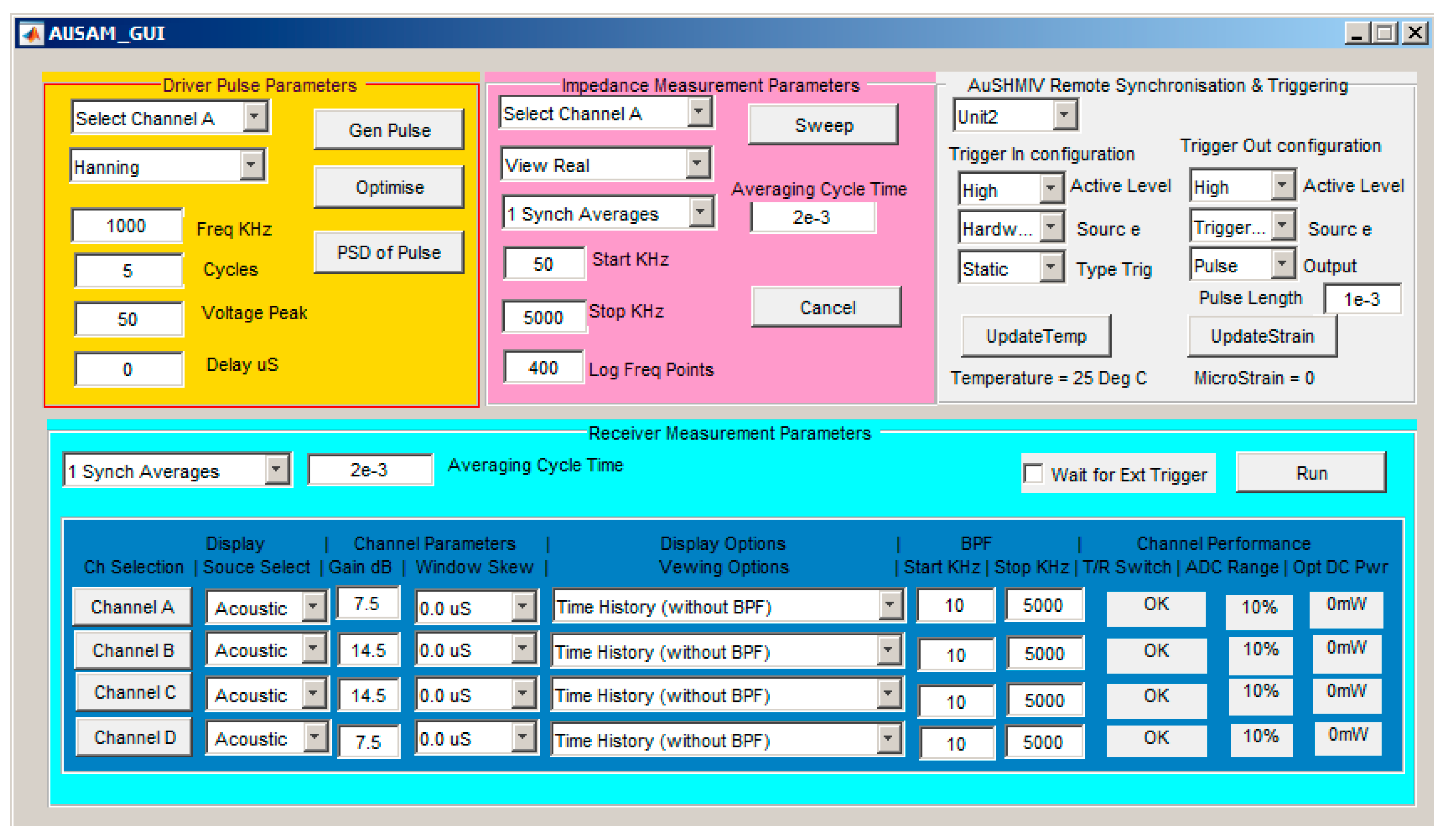
Figure 10.
Example Graphical User Interface (GUI) created to explore the AUSAM+ capability.
Figure 10.
Example Graphical User Interface (GUI) created to explore the AUSAM+ capability.
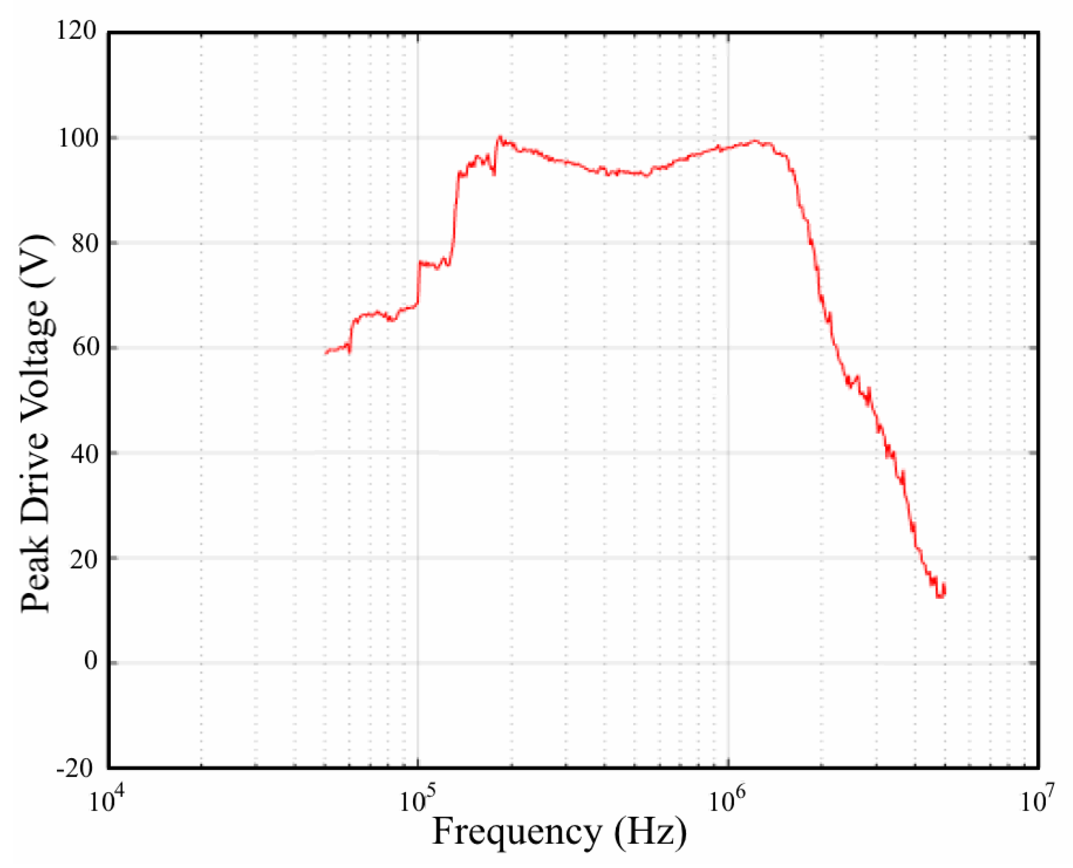
Figure 11.
Typical variation in maximum excitation peak voltage with various excitation frequencies applied over a precision 1 nF capacitor.
Figure 11.
Typical variation in maximum excitation peak voltage with various excitation frequencies applied over a precision 1 nF capacitor.
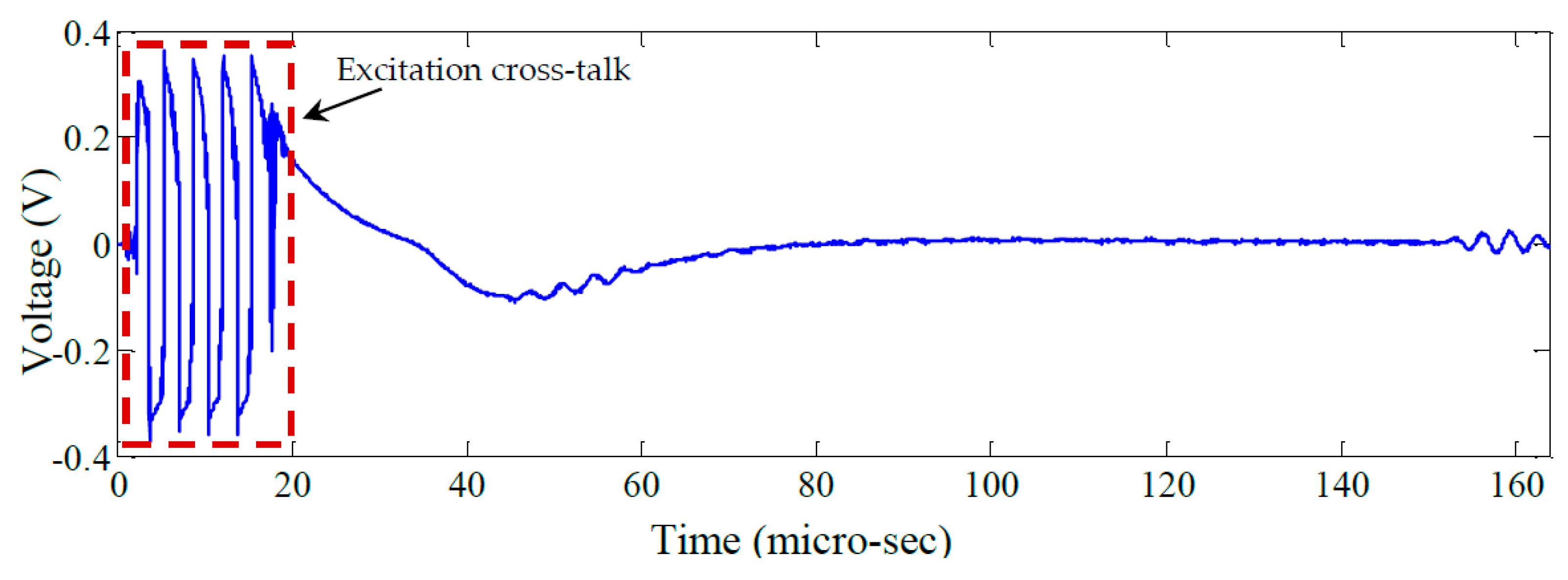
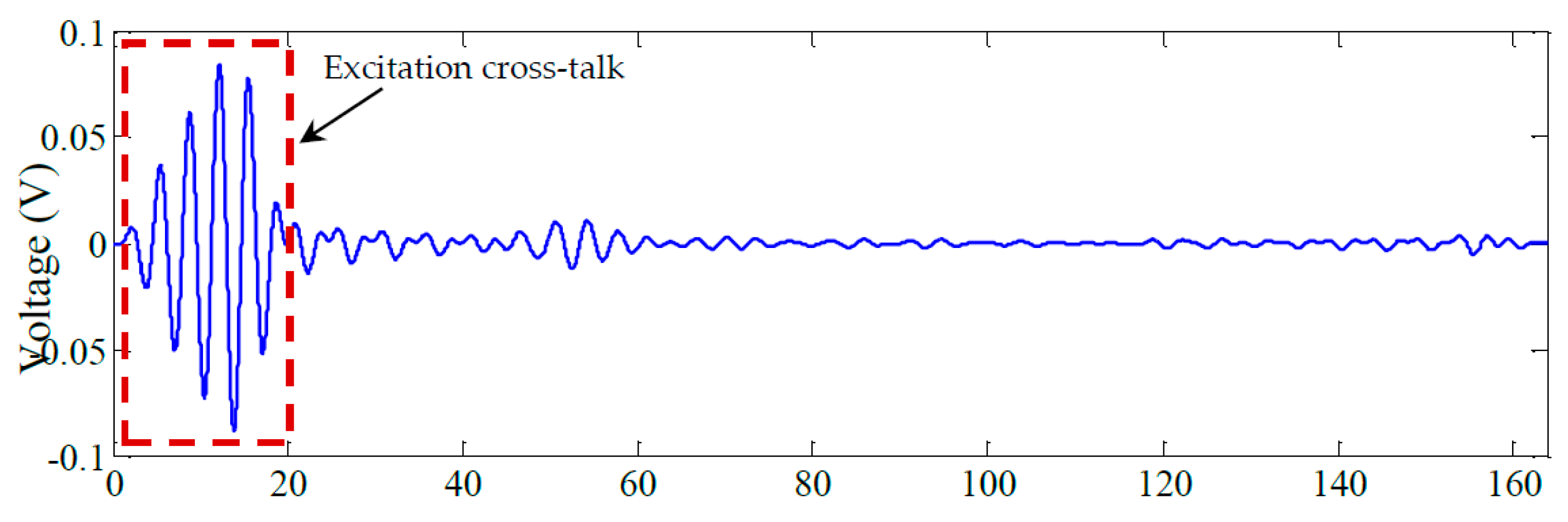
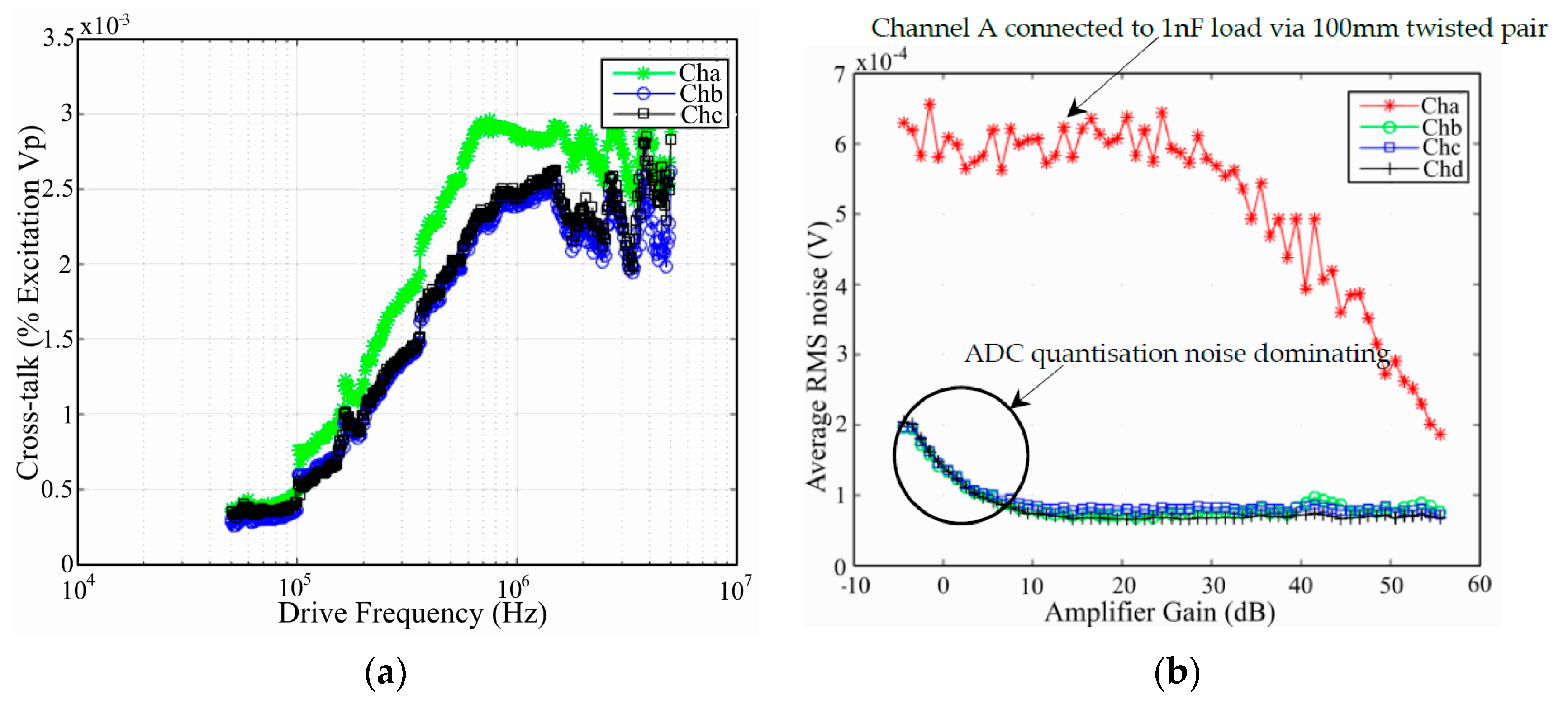
Figure 12.
(a) Percentage of channel D excitation cross-talk on other channels; (b) Typical single-shot (no synchronous averaging) Root Mean Square (RMS) noise floor performance.
Figure 12.
(a) Percentage of channel D excitation cross-talk on other channels; (b) Typical single-shot (no synchronous averaging) Root Mean Square (RMS) noise floor performance.
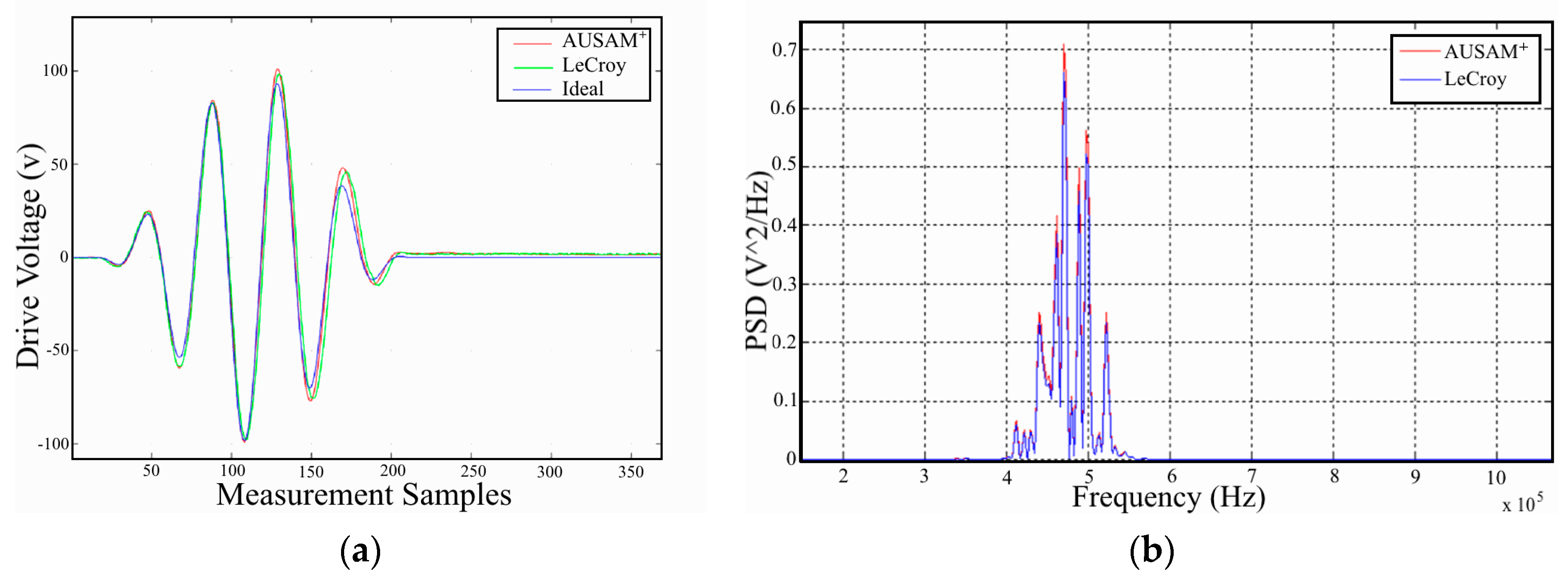
Figure 13.
Acquisition system comparison to a LeCroy oscilloscope in both Drive Monitor mode and pitch-catch regime; (a) 1.2 MHz 100 Vpeak excitation signal applied to a 1 nF capacitor; (b) The PSD of the AU response of a PWAS on an aluminum panel, in a pitch-catch regime, when excited at 500 kHz.
Figure 13.
Acquisition system comparison to a LeCroy oscilloscope in both Drive Monitor mode and pitch-catch regime; (a) 1.2 MHz 100 Vpeak excitation signal applied to a 1 nF capacitor; (b) The PSD of the AU response of a PWAS on an aluminum panel, in a pitch-catch regime, when excited at 500 kHz.
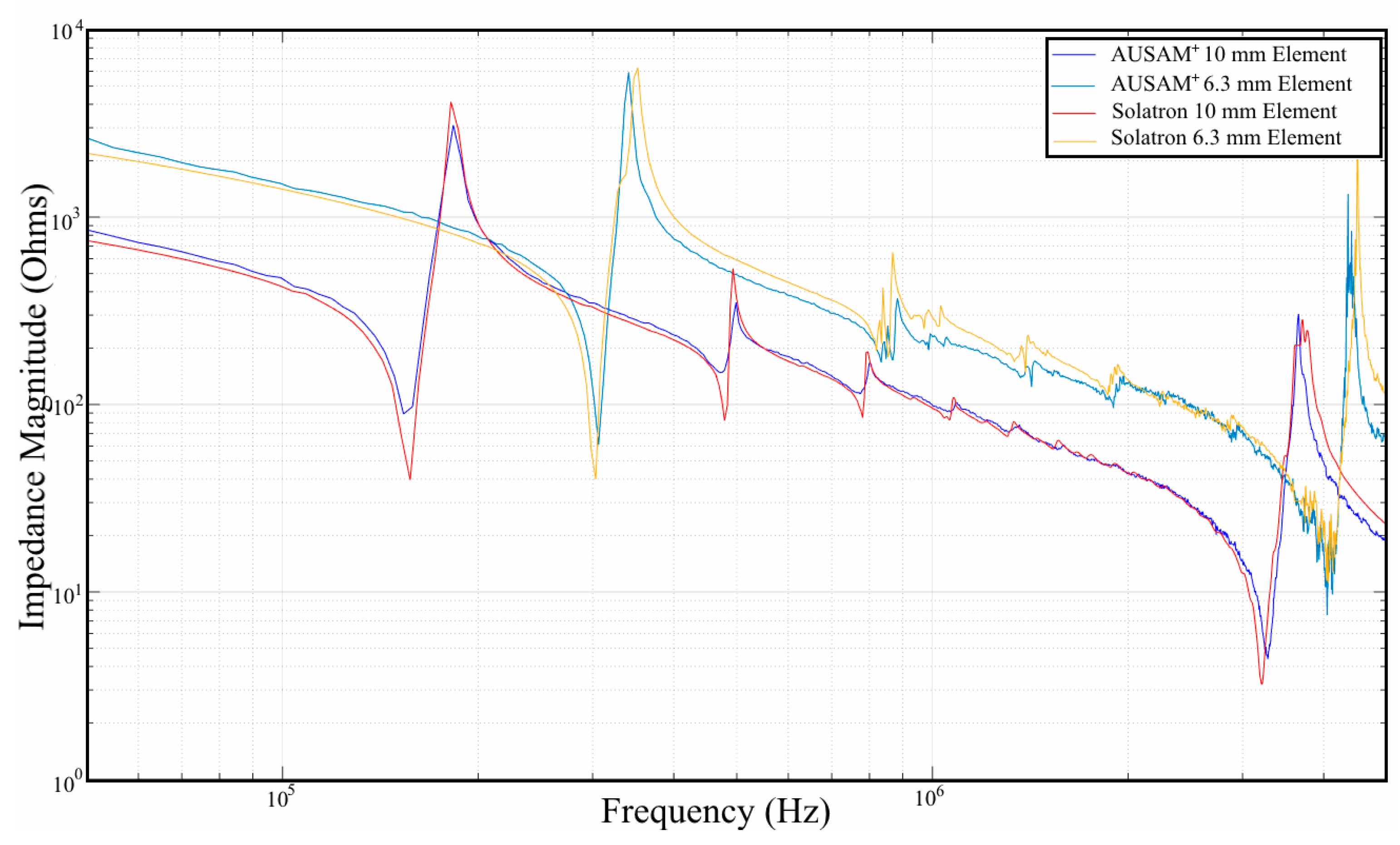
Figure 14.
Comparison of the EM impedance magnitude sweep over the AUSAM+ bandwidth for un-bonded 6.3 mm and 10 mm diameter PWAS elements.
Figure 14.
Comparison of the EM impedance magnitude sweep over the AUSAM+ bandwidth for un-bonded 6.3 mm and 10 mm diameter PWAS elements.
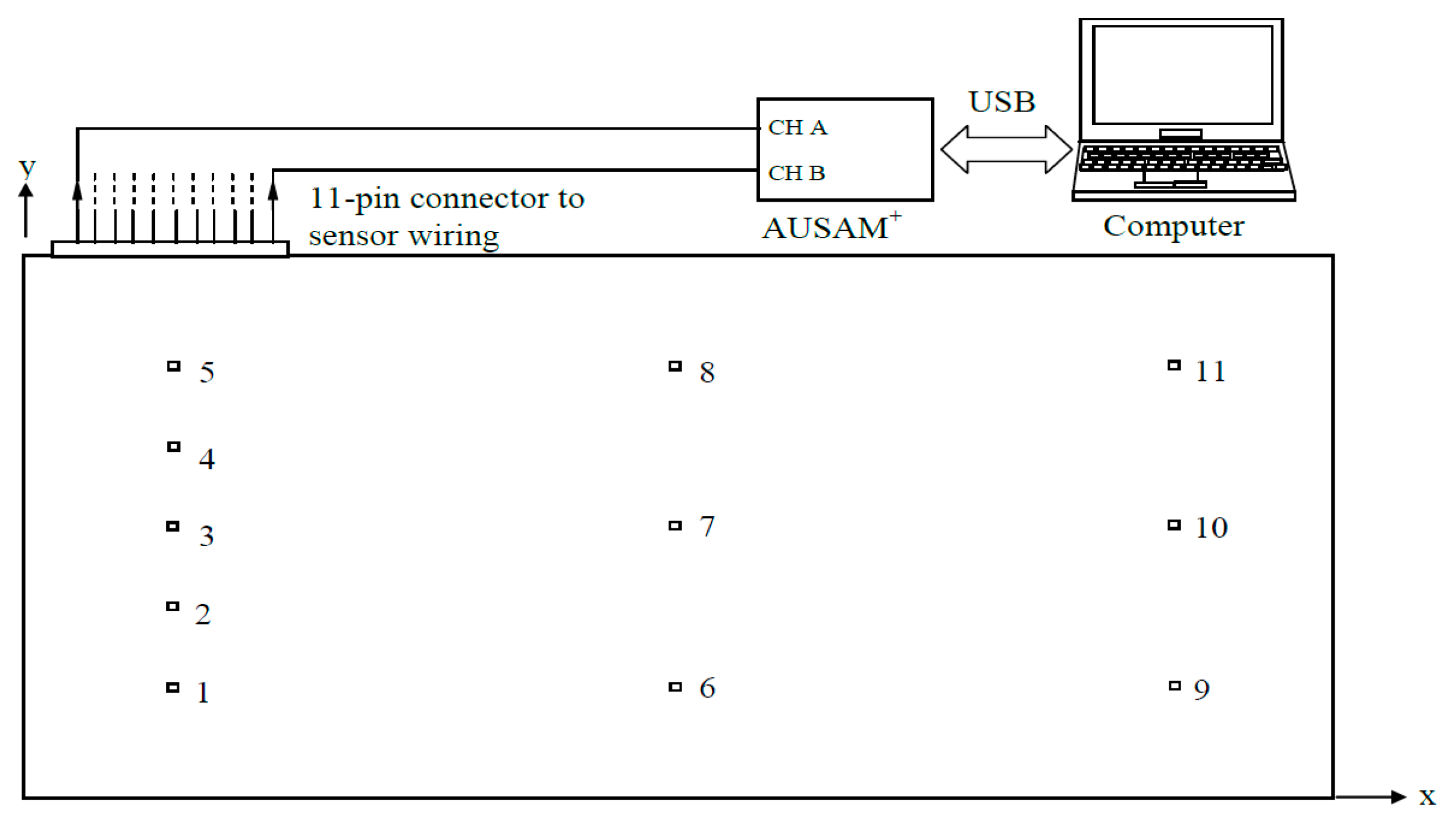
Figure 15.
Schematic of experimental setup showing rectangular PWAS grid arrangement.
Figure 15.
Schematic of experimental setup showing rectangular PWAS grid arrangement.
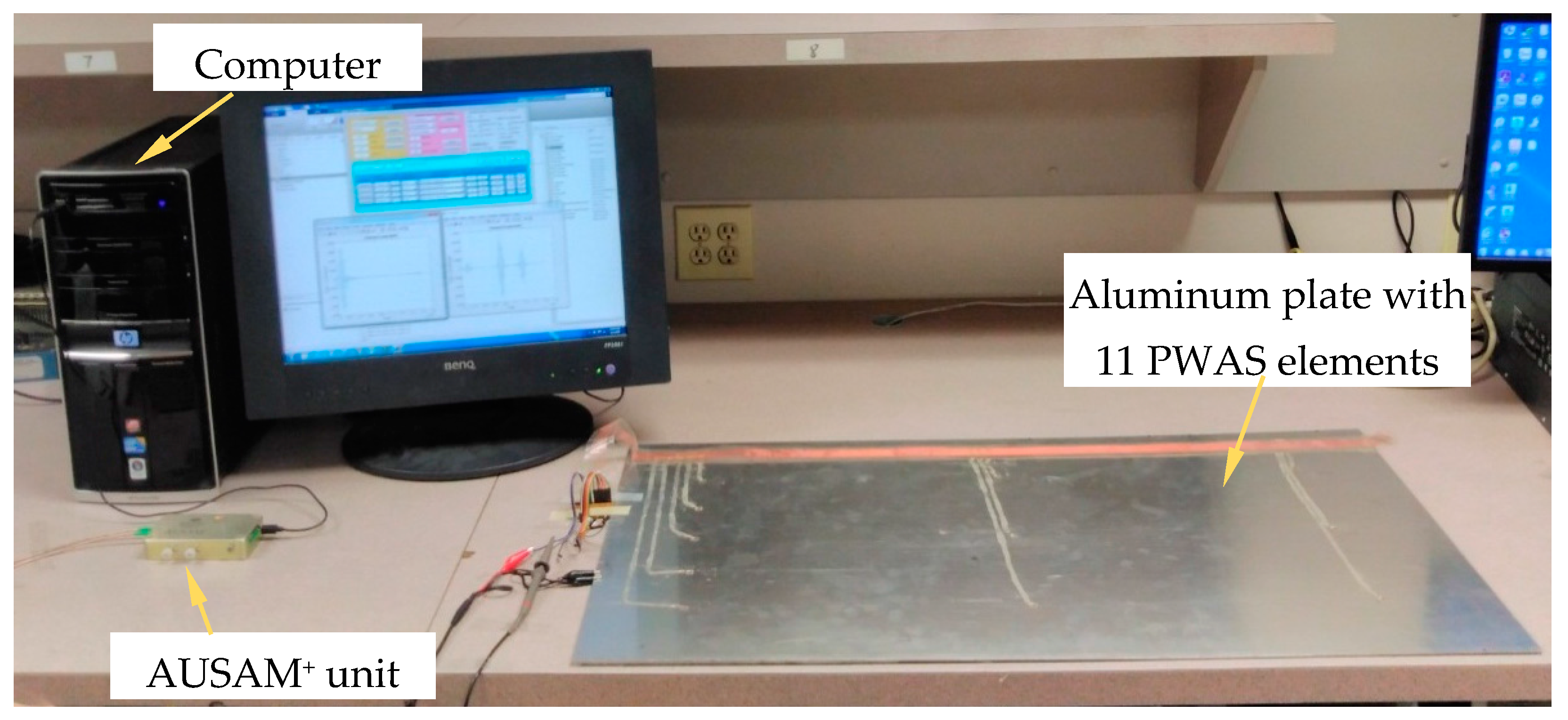
Figure 16.
Image of the experimental setup.
Figure 16.
Image of the experimental setup.
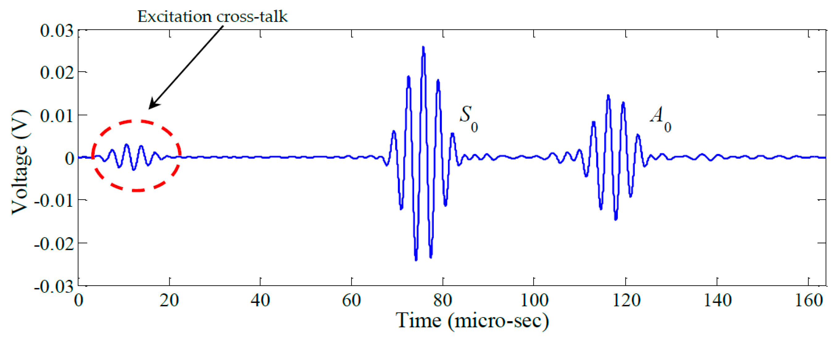
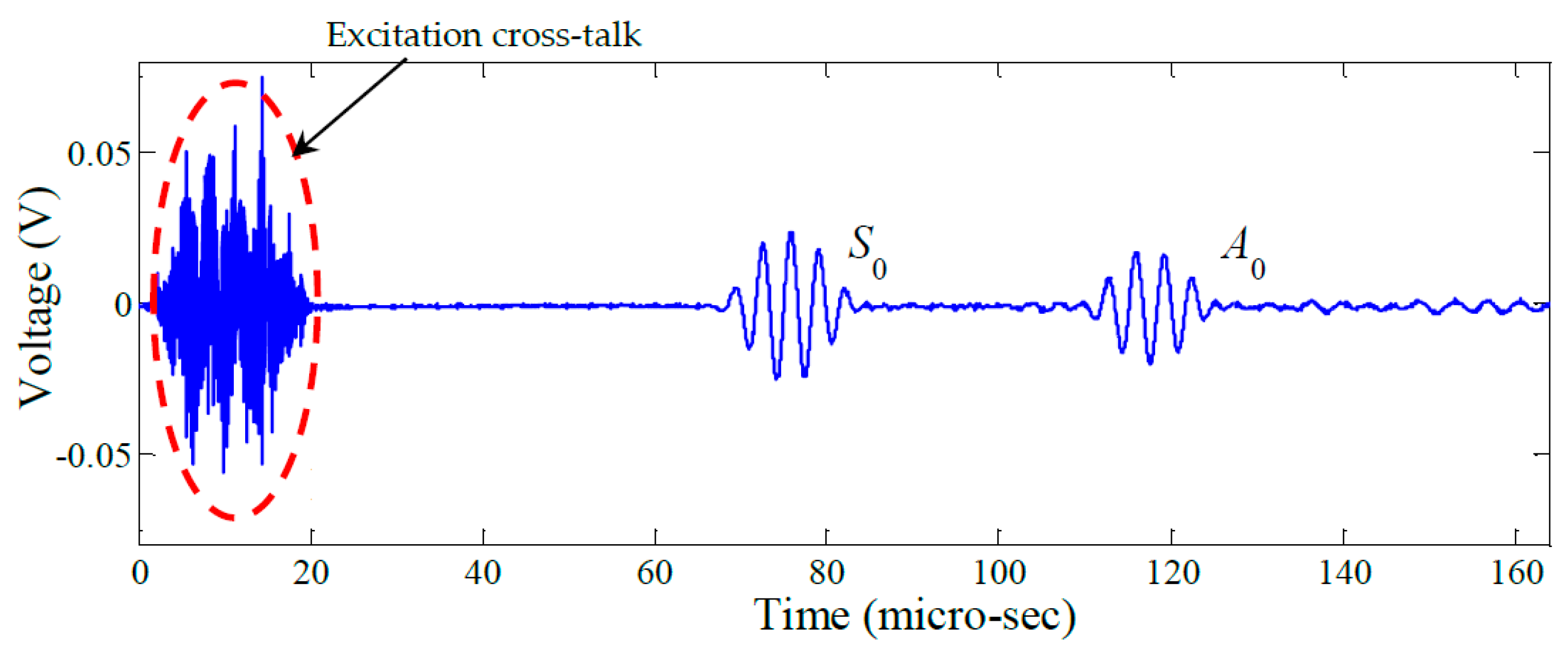
Figure 17.
Typical signal acquired using the AUSAM+ (PWAS 8).
Figure 17.
Typical signal acquired using the AUSAM+ (PWAS 8).
Figure 18.
Signal band-pass filtered between 200 kHz and 400 kHz.
Figure 18.
Signal band-pass filtered between 200 kHz and 400 kHz.
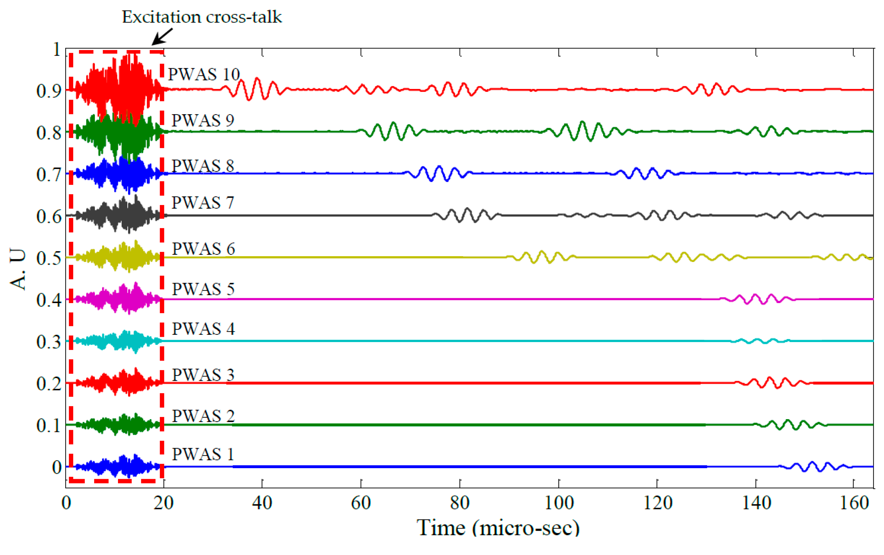
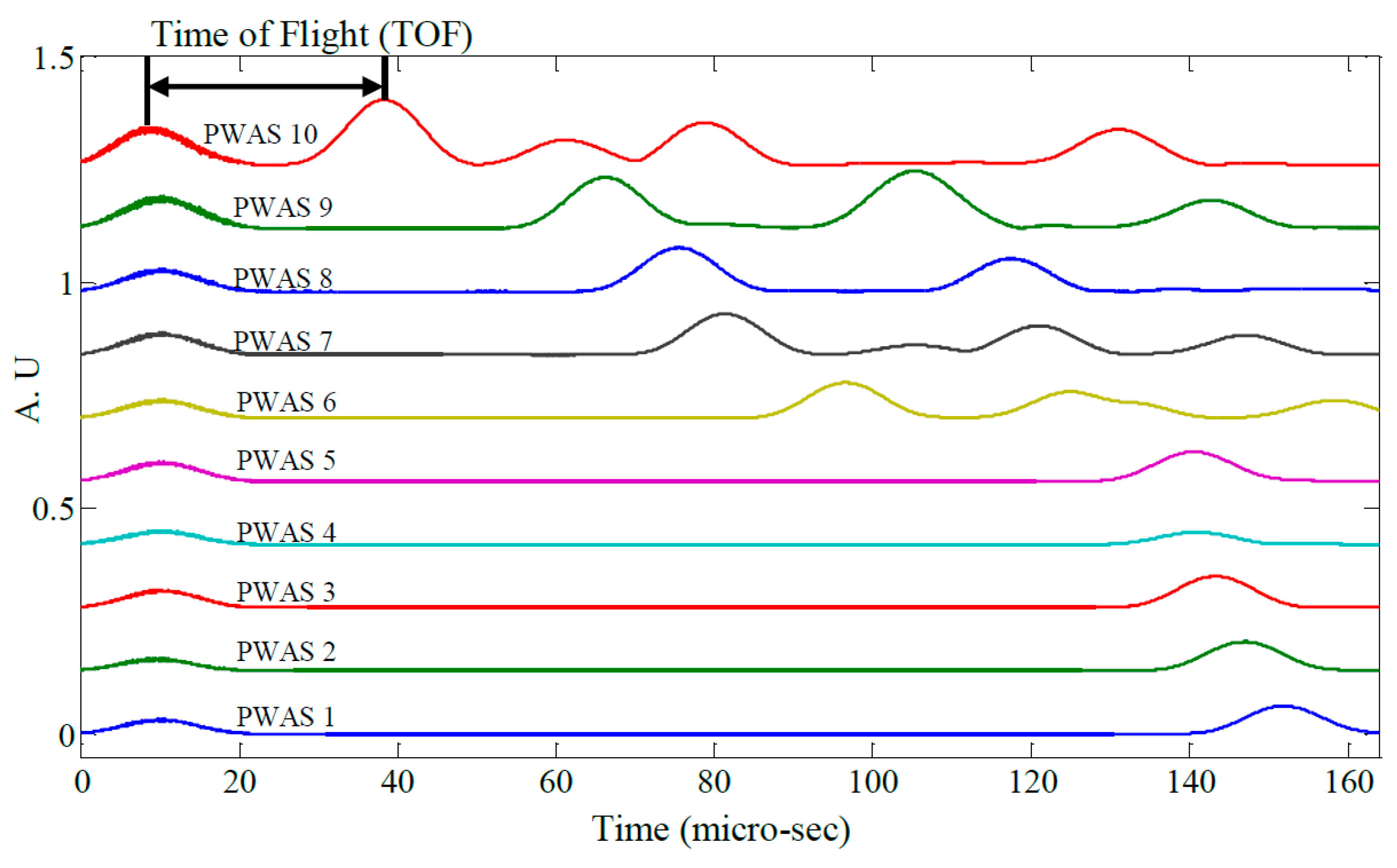
Figure 19.
Raw signals from PWAS 1–10.
Figure 19.
Raw signals from PWAS 1–10.
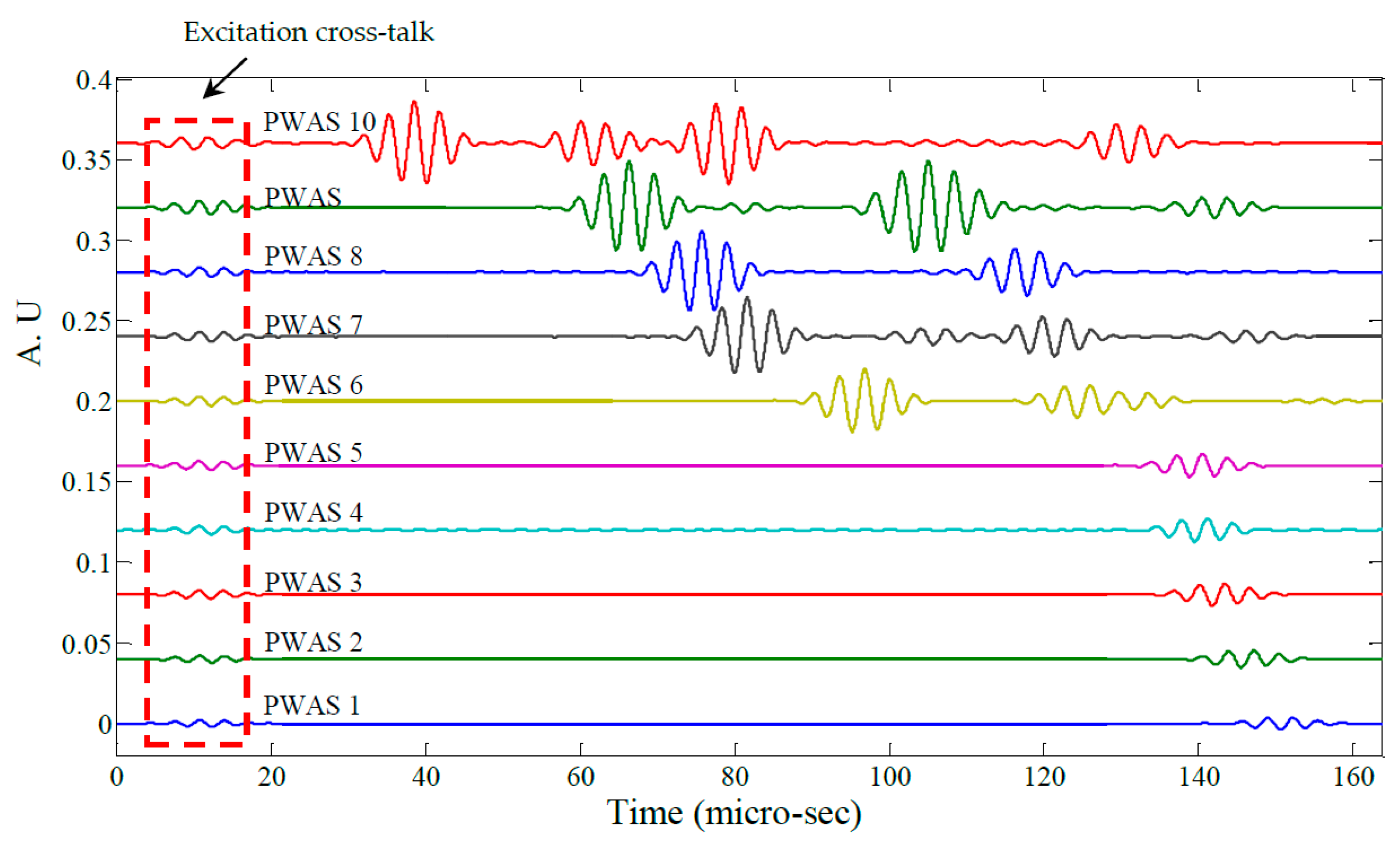
Figure 20.
Filtered signals from PWAS 1–10.
Figure 20.
Filtered signals from PWAS 1–10.
Figure 21.
Signal envelopes of PWAS 1–10.
Figure 21.
Signal envelopes of PWAS 1–10.
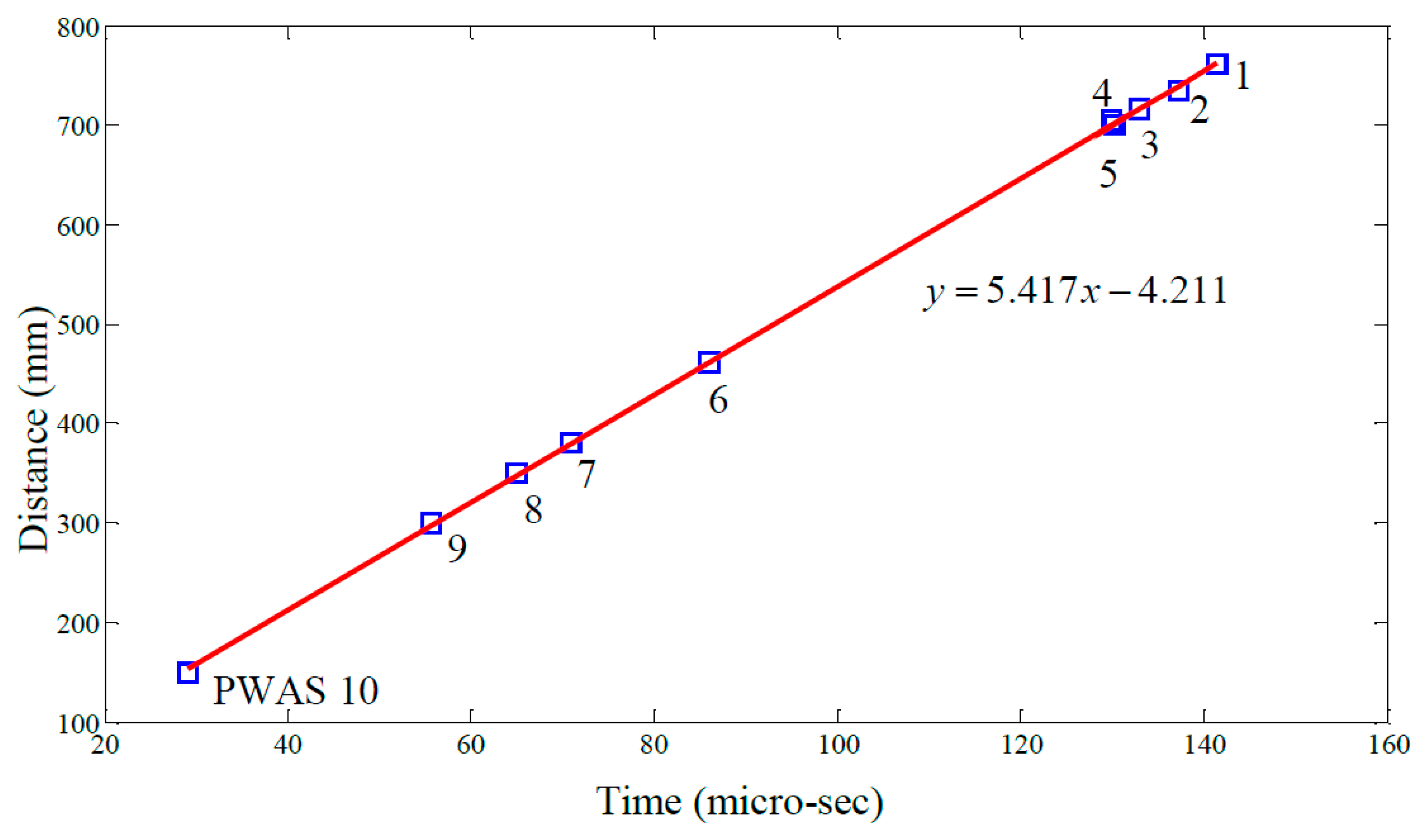
Figure 22.
Correlation between radial distance and time of flight.
Figure 22.
Correlation between radial distance and time of flight.
Figure 23.
The unfiltered pulse-echo signal on PWAS 11.
Figure 23.
The unfiltered pulse-echo signal on PWAS 11.
Figure 24.
The filtered signal on PWAS 11.
Figure 24.
The filtered signal on PWAS 11.
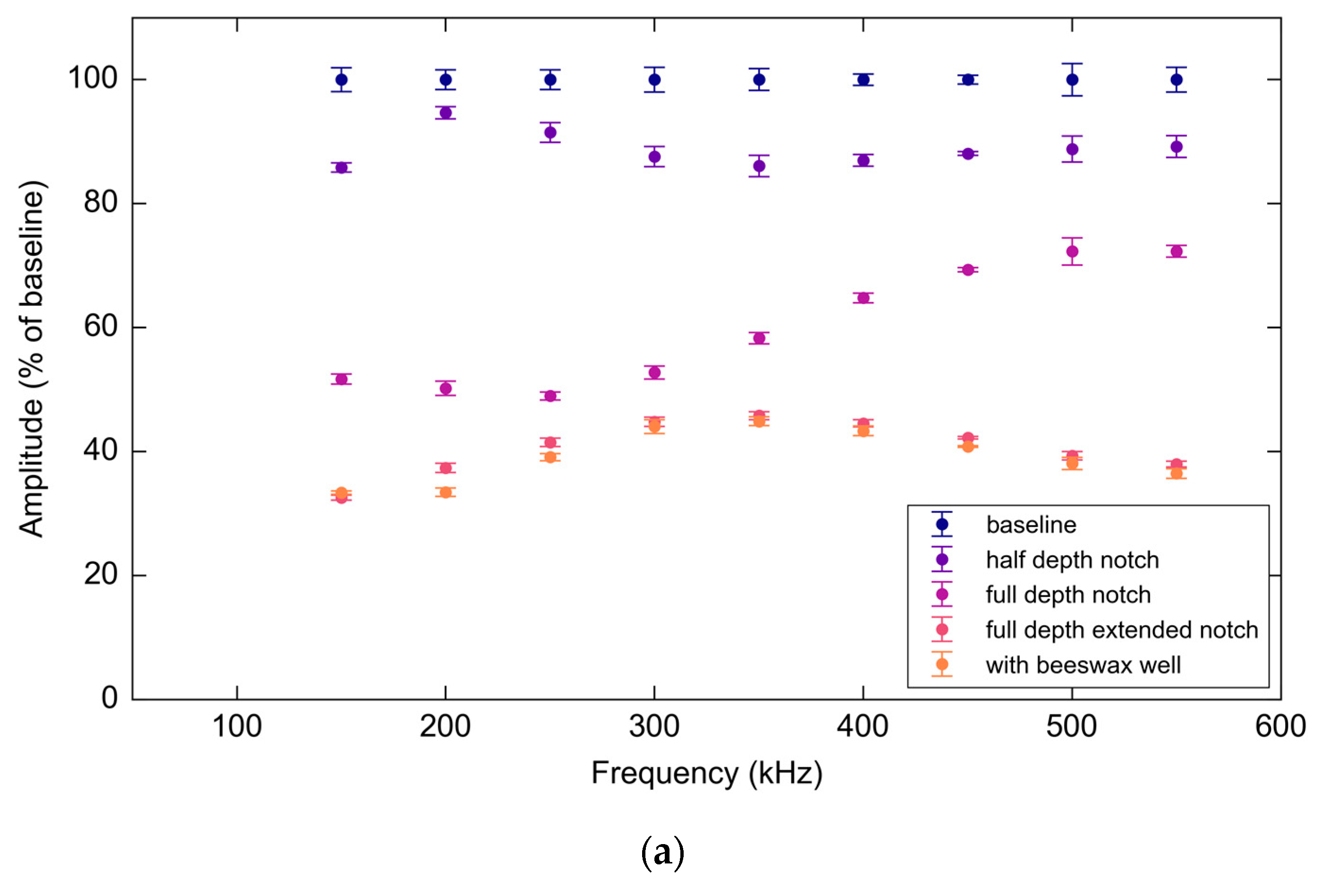
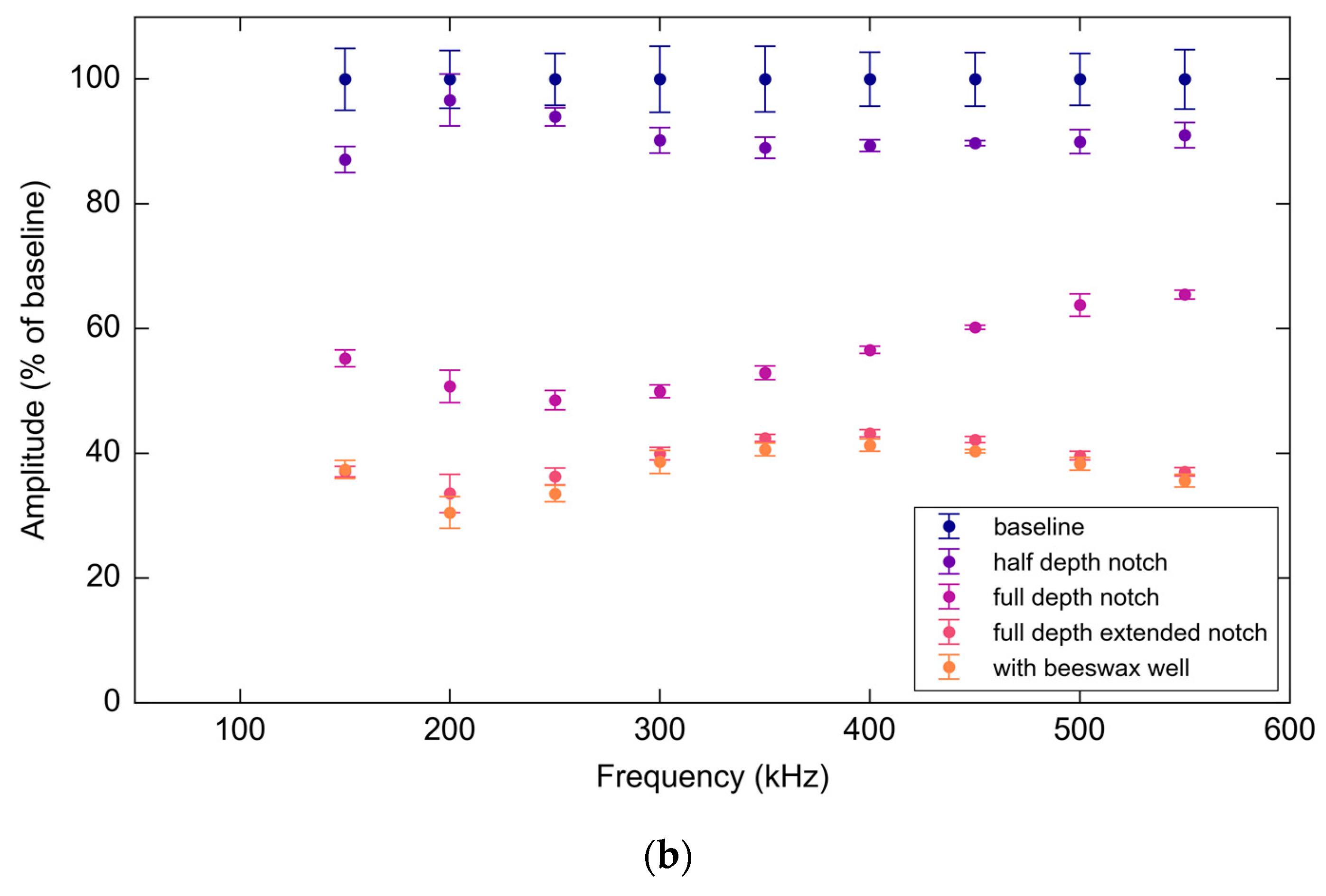
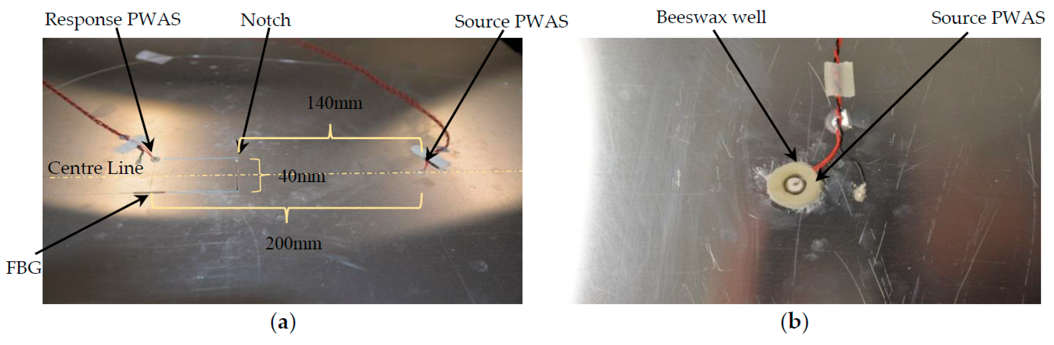
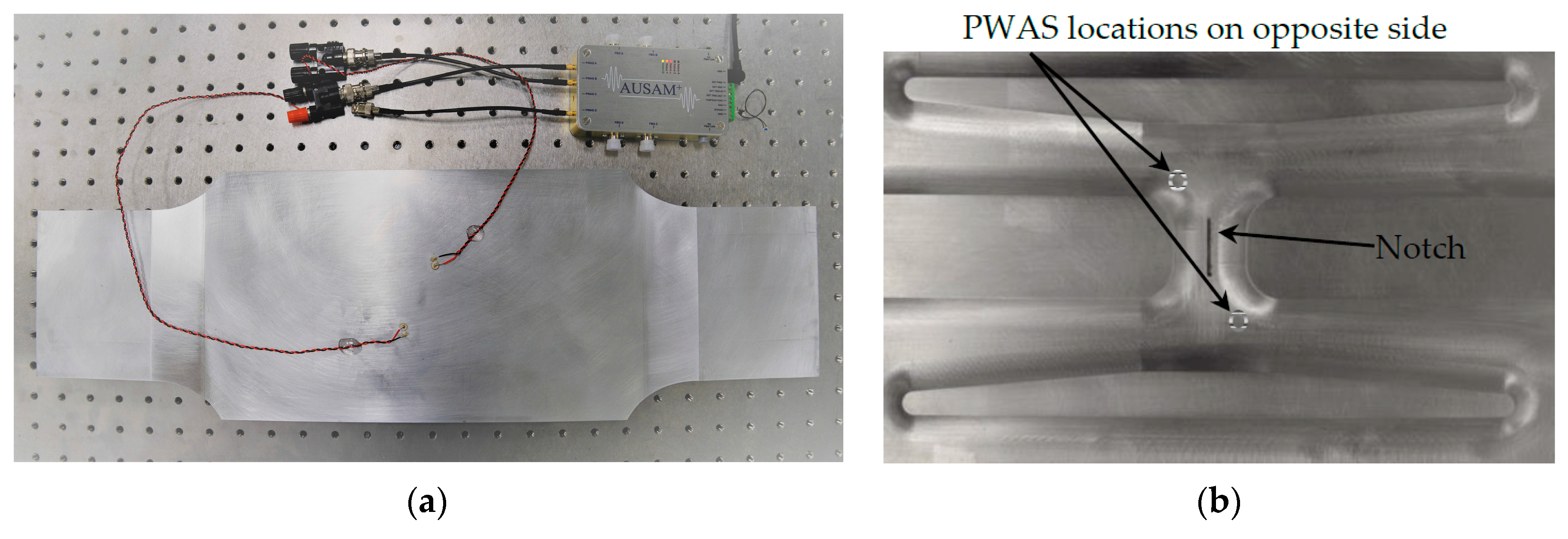
Figure 25.
(a) An aluminum panel with 40 mm long full-depth extended notch located 140 mm from the source PWAS and perpendicular to the center line; (b) Photograph of the Beeswax well around the source PWAS to contain acetone solution used to induce damage of the bond layer.
Figure 25.
(a) An aluminum panel with 40 mm long full-depth extended notch located 140 mm from the source PWAS and perpendicular to the center line; (b) Photograph of the Beeswax well around the source PWAS to contain acetone solution used to induce damage of the bond layer.
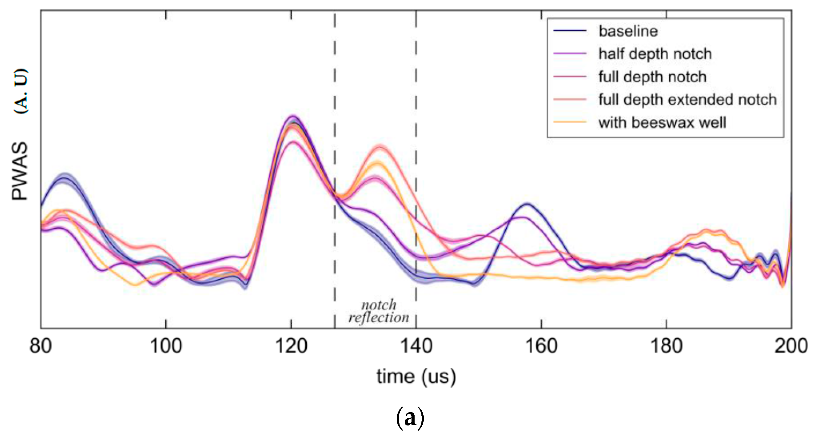
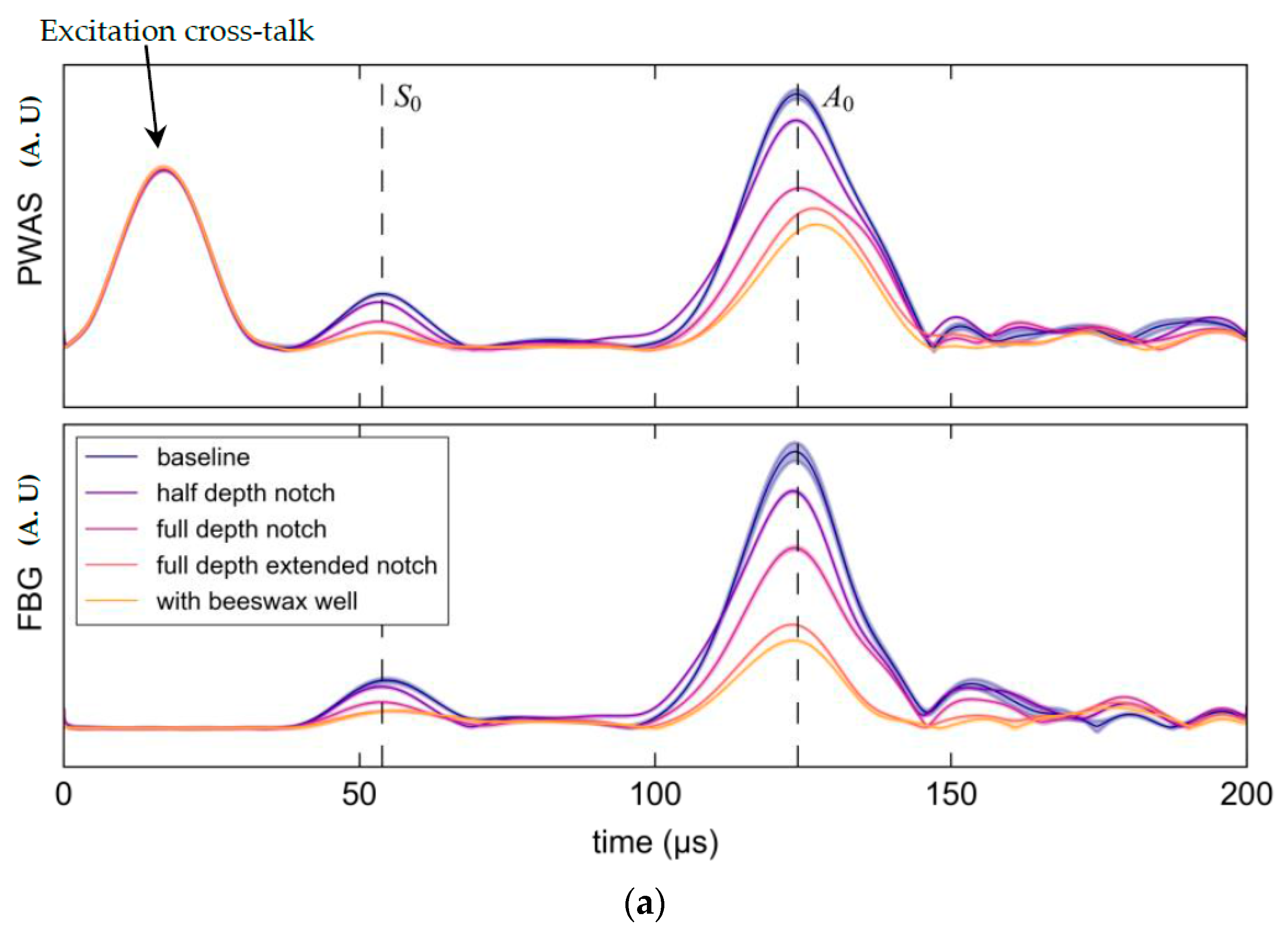
Figure 26.
Hilbert transform envelops of the response PWAS and Fiber Bragg Gratings (FBG) showing the average and two standard deviations (shaded) for each stage in the experiment. (a) 150 kHz excitation; (b) 550 kHz excitation.
Figure 26.
Hilbert transform envelops of the response PWAS and Fiber Bragg Gratings (FBG) showing the average and two standard deviations (shaded) for each stage in the experiment. (a) 150 kHz excitation; (b) 550 kHz excitation.
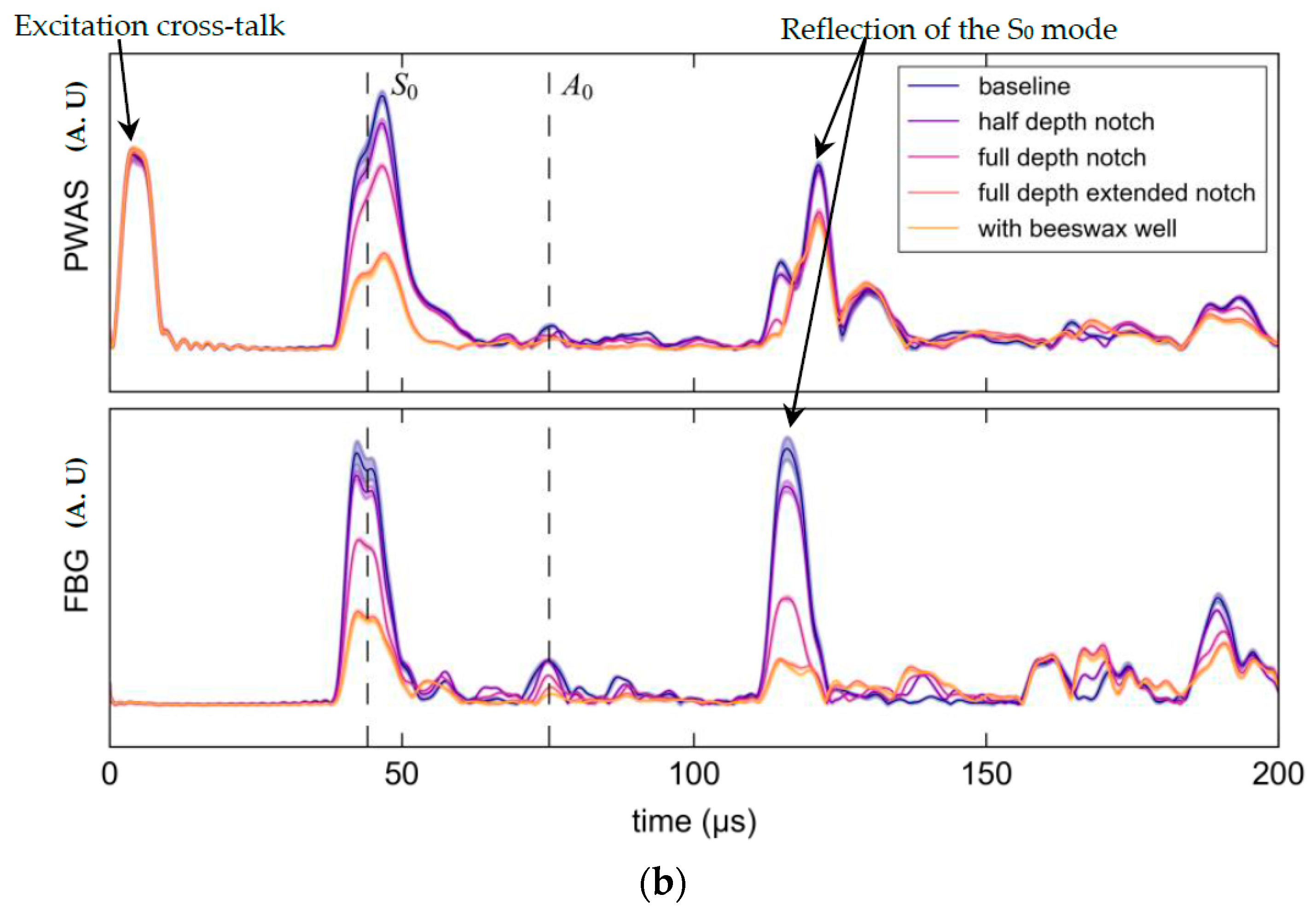
Figure 27.
(a) PWAS S0 mode amplitudes normalized as a percentage of the baseline average peak over frequencies and experimental stages; (b) FBG S0 mode amplitudes normalized as a percentage of the baseline average peak over frequencies and experimental stages.
Figure 27.
(a) PWAS S0 mode amplitudes normalized as a percentage of the baseline average peak over frequencies and experimental stages; (b) FBG S0 mode amplitudes normalized as a percentage of the baseline average peak over frequencies and experimental stages.
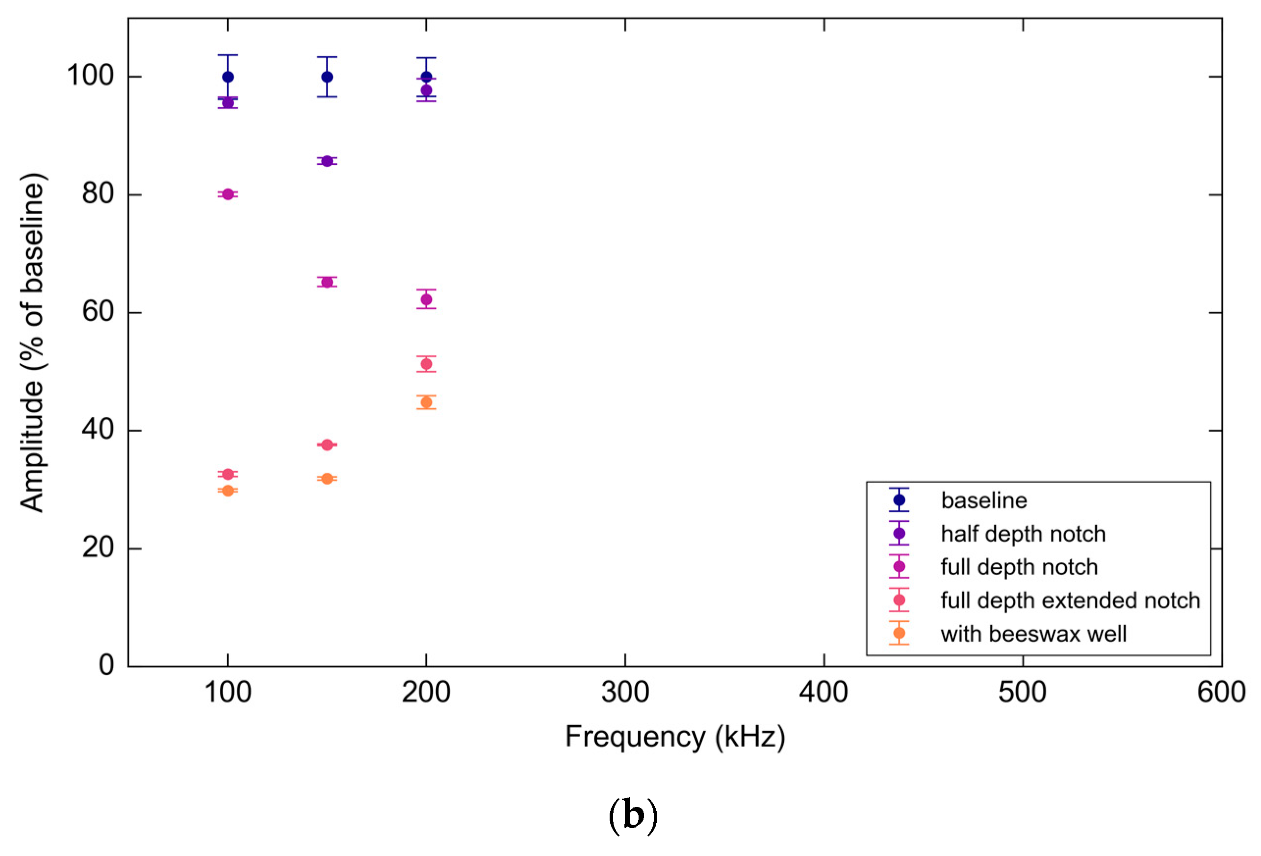
Figure 28.
(a) PWAS A0 mode amplitudes normalized as a percentage of the baseline average peak over frequencies and experimental stages; (b) FBG A0 mode amplitudes normalized as a percentage of the baseline average peak over frequencies and experimental stages.
Figure 28.
(a) PWAS A0 mode amplitudes normalized as a percentage of the baseline average peak over frequencies and experimental stages; (b) FBG A0 mode amplitudes normalized as a percentage of the baseline average peak over frequencies and experimental stages.
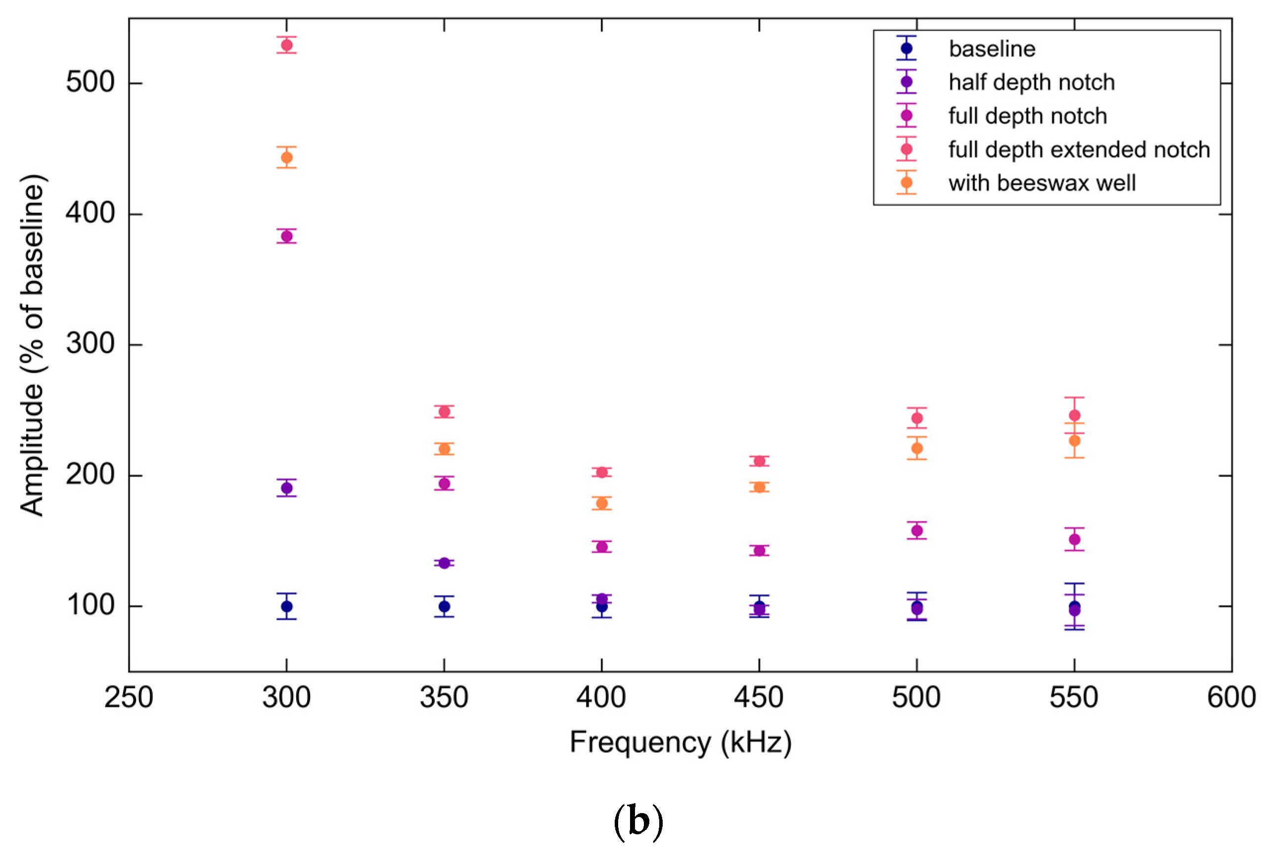
Figure 29.
(a) Pulse-echo signal peak bordered by dashed lines corresponds to a reflection from the notch for each stage in the experiment with two standard deviations (shaded); (b) The same reflection Pulse-echo signal peak amplitudes normalized as a percentage of the baseline average peak over frequencies and experimental stages.
Figure 30.
(a) Successive pitch-catch responses from dark (purple) to light (orange) at 150 kHz showing a gradual attenuation as the source element bond-line was damaged by acetone; (b) Successive impedance magnitude plots from dark (purple) to light (orange) showing an increase in capacitance at the lateral resonance peak indicating de-bonding of the source element.
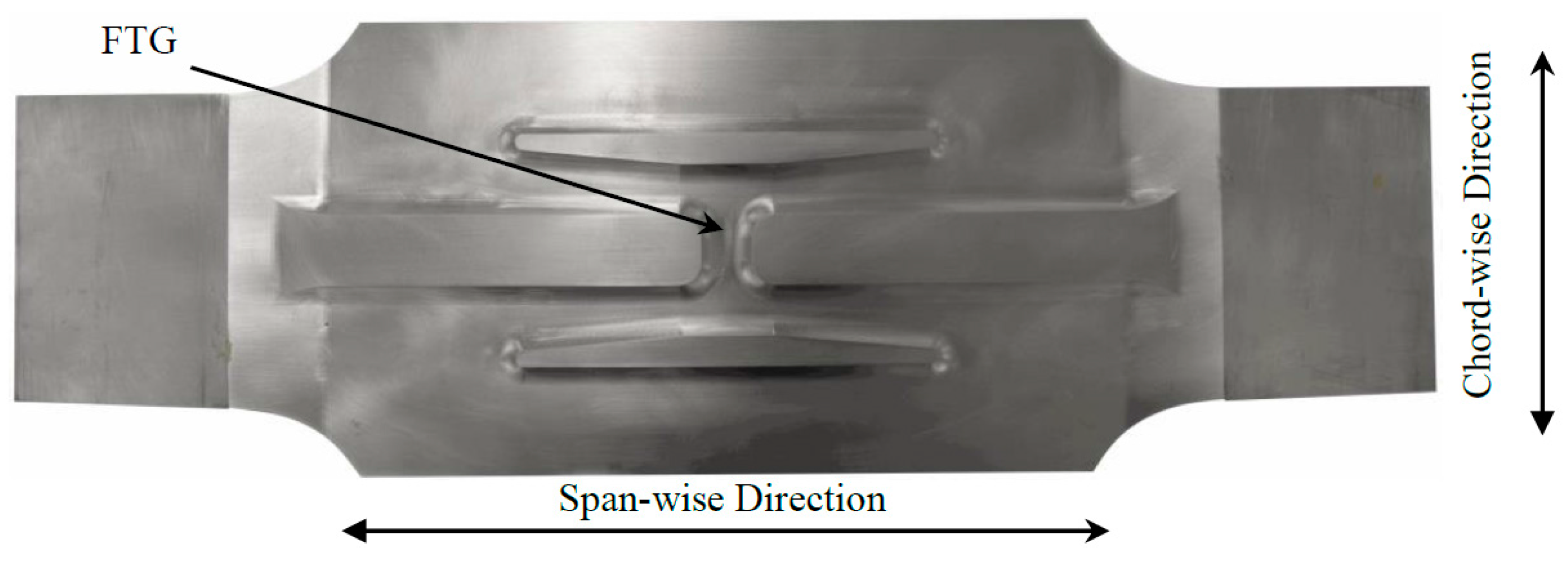
Figure 31.
Test coupon representing key structural elements of F-111C lower wing skin at Forward Auxiliary Spar Station (FASS) 281.28. Marked is the location of the Fuel Transfer Groove (FTG).
Figure 31.
Test coupon representing key structural elements of F-111C lower wing skin at Forward Auxiliary Spar Station (FASS) 281.28. Marked is the location of the Fuel Transfer Groove (FTG).
Figure 32.
(a) The FASS coupon test set up showing two PWAS elements installed on the outside of the wing skin; (b) The notch milled into the FTG location after establishing a baseline to simulate where a crack typically forms under operational loading. Shaded marks show the location of PWAS elements bonded on the opposite side.
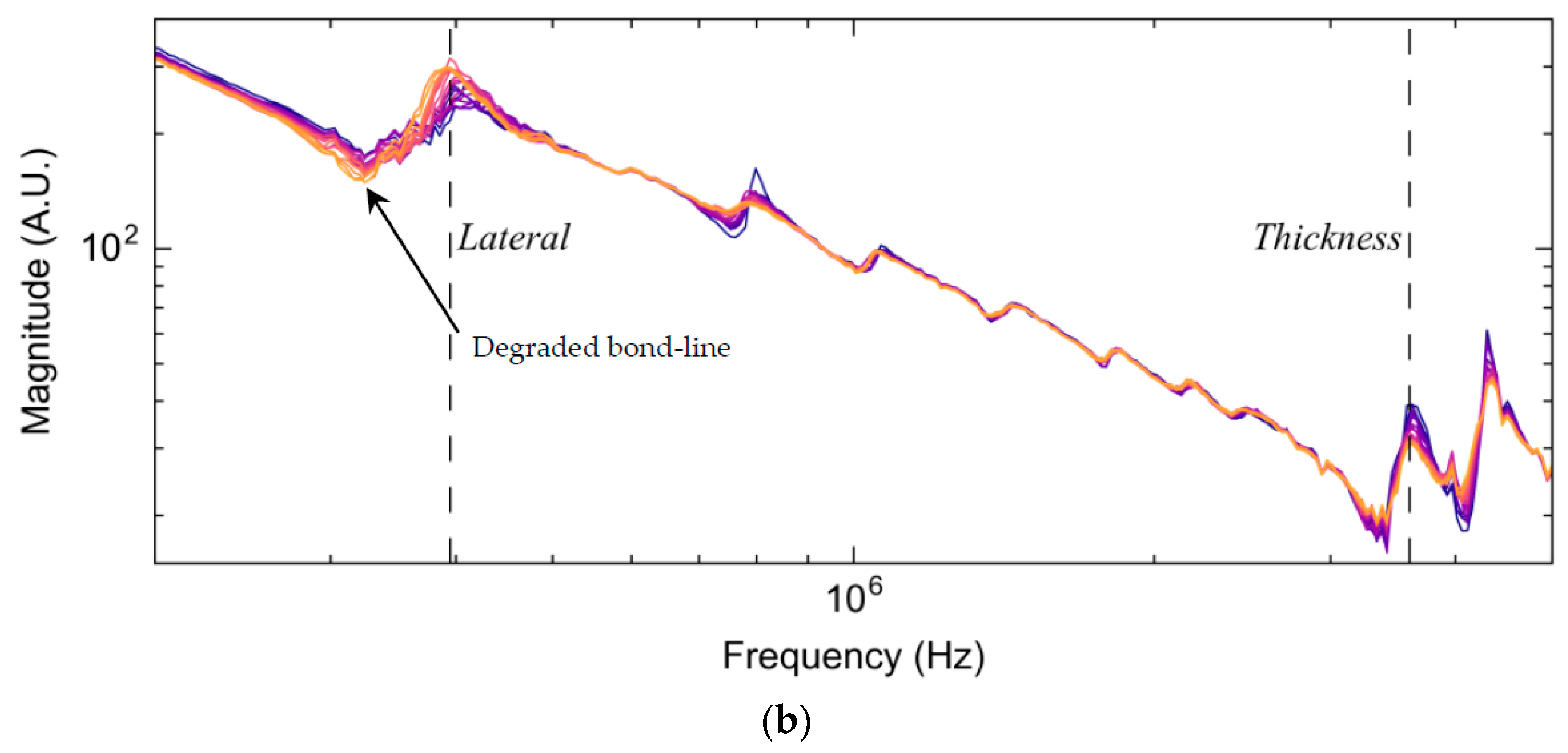
Figure 33.
Effect of the notch on the pitch-catch response at 1.25 MHz with the first incident wave-packet bordered by dashed lines. The barely perceptible shading confirms very good repeatability.
Figure 33.
Effect of the notch on the pitch-catch response at 1.25 MHz with the first incident wave-packet bordered by dashed lines. The barely perceptible shading confirms very good repeatability.
Figure 34.
Variation in attenuation expressed as a percentage of the baseline calculated using a Riemann sum of the signal envelope for the first wave-packet over the experimental frequency range. Error bars represent two standard deviations over ten consecutive sweeps.
Figure 34.
Variation in attenuation expressed as a percentage of the baseline calculated using a Riemann sum of the signal envelope for the first wave-packet over the experimental frequency range. Error bars represent two standard deviations over ten consecutive sweeps.
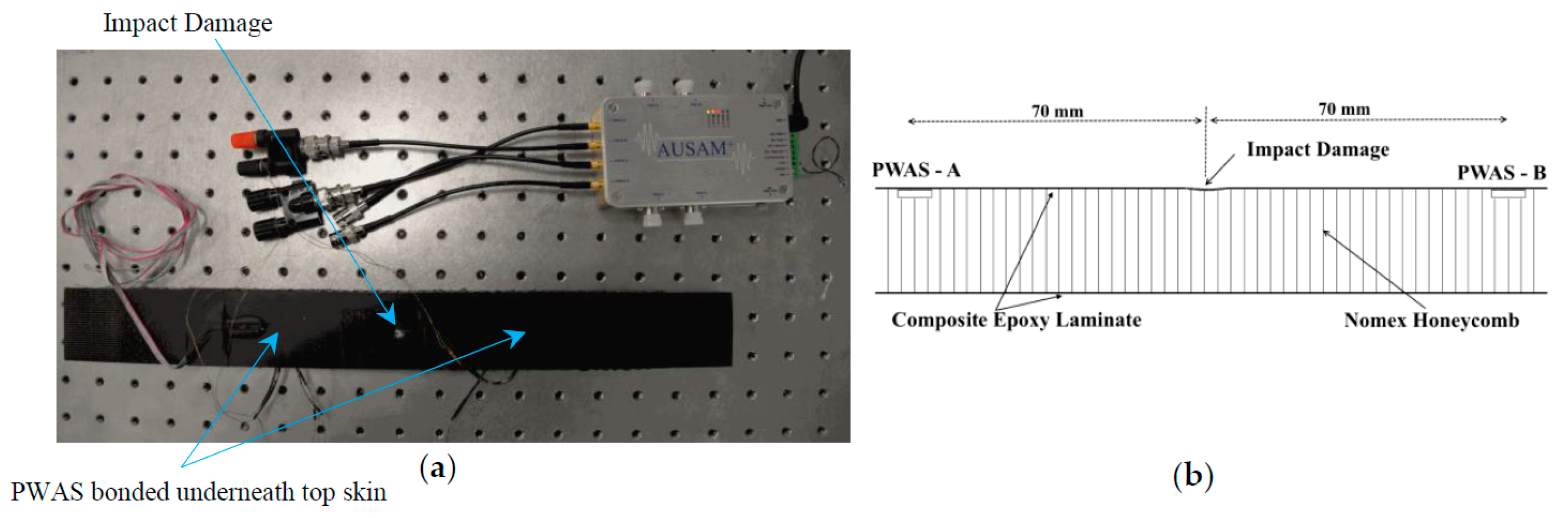
Figure 35.
Composite test set-up. (a) Interrogating the impacted coupon; (b) coupon cross-sectional view showing the location of two embedded PWAS elements in relation to the impact site.
Figure 35.
Composite test set-up. (a) Interrogating the impacted coupon; (b) coupon cross-sectional view showing the location of two embedded PWAS elements in relation to the impact site.
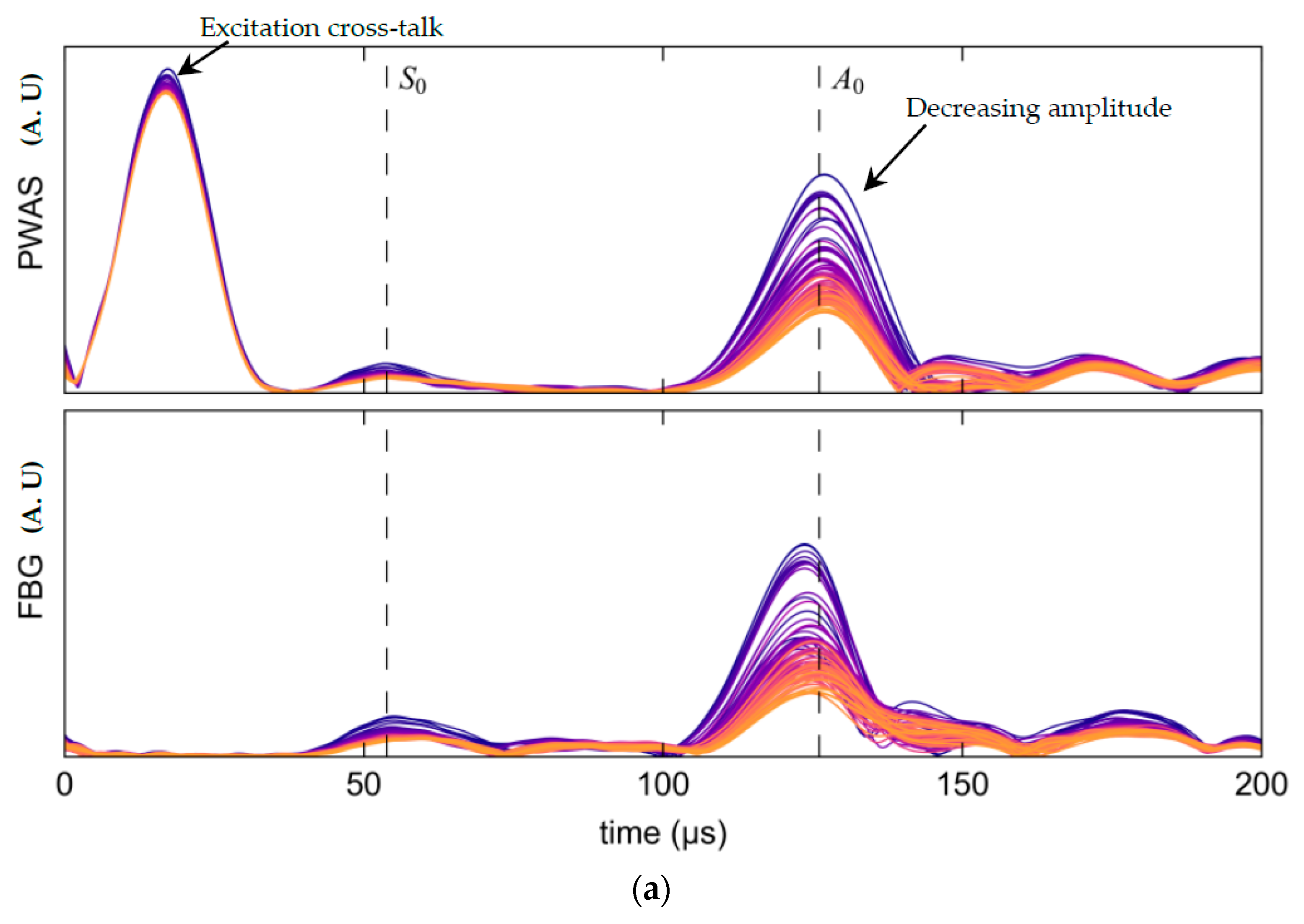
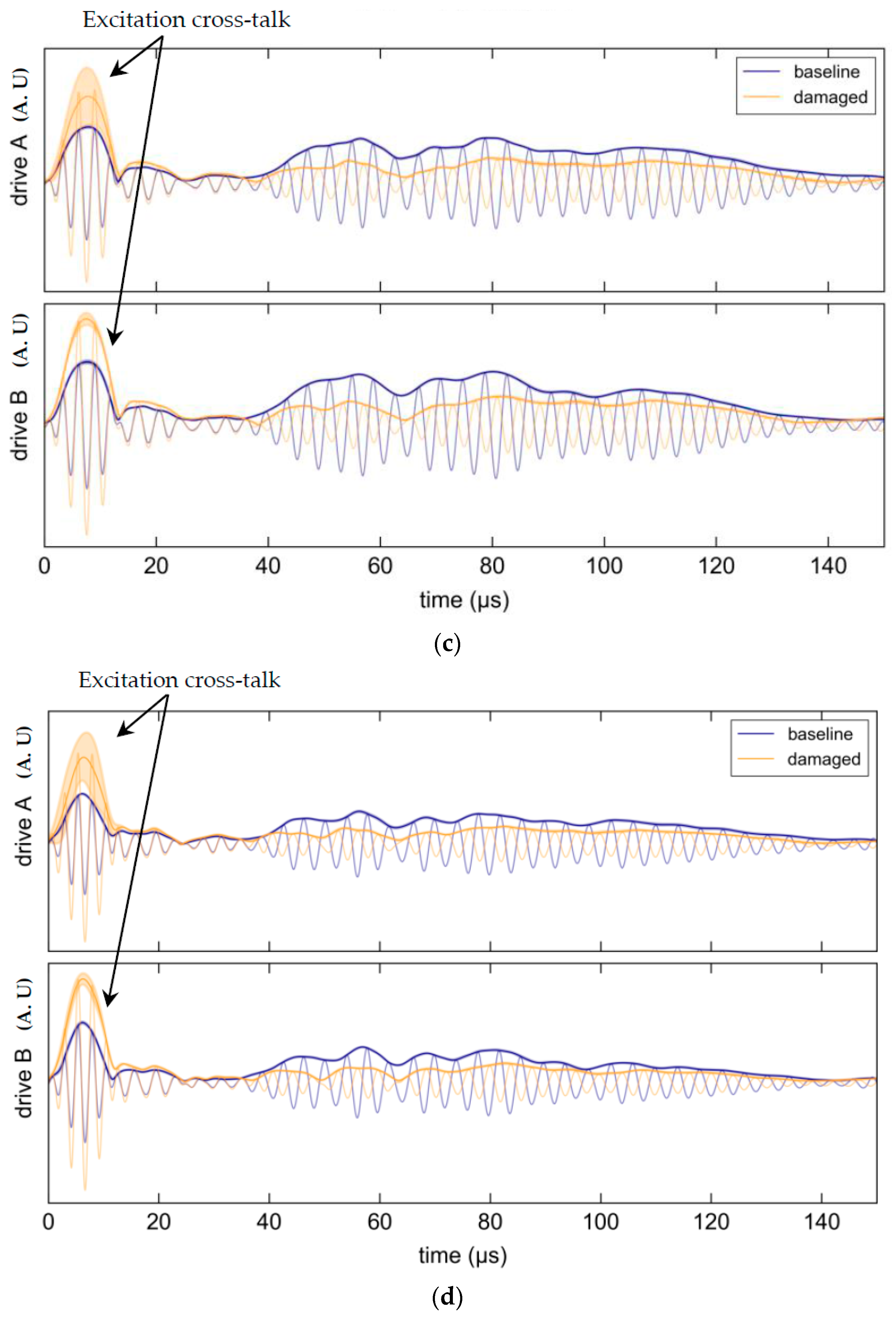
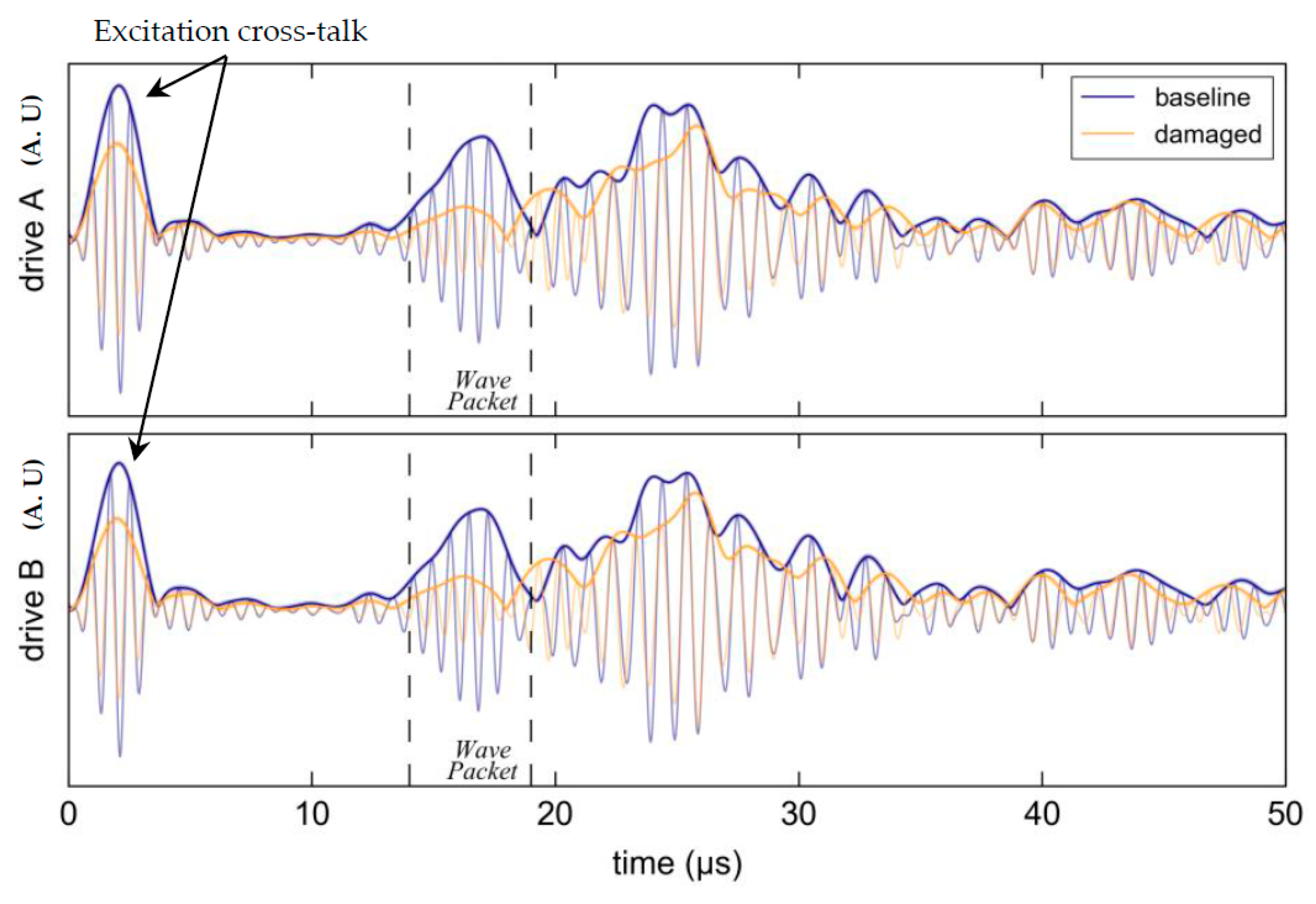
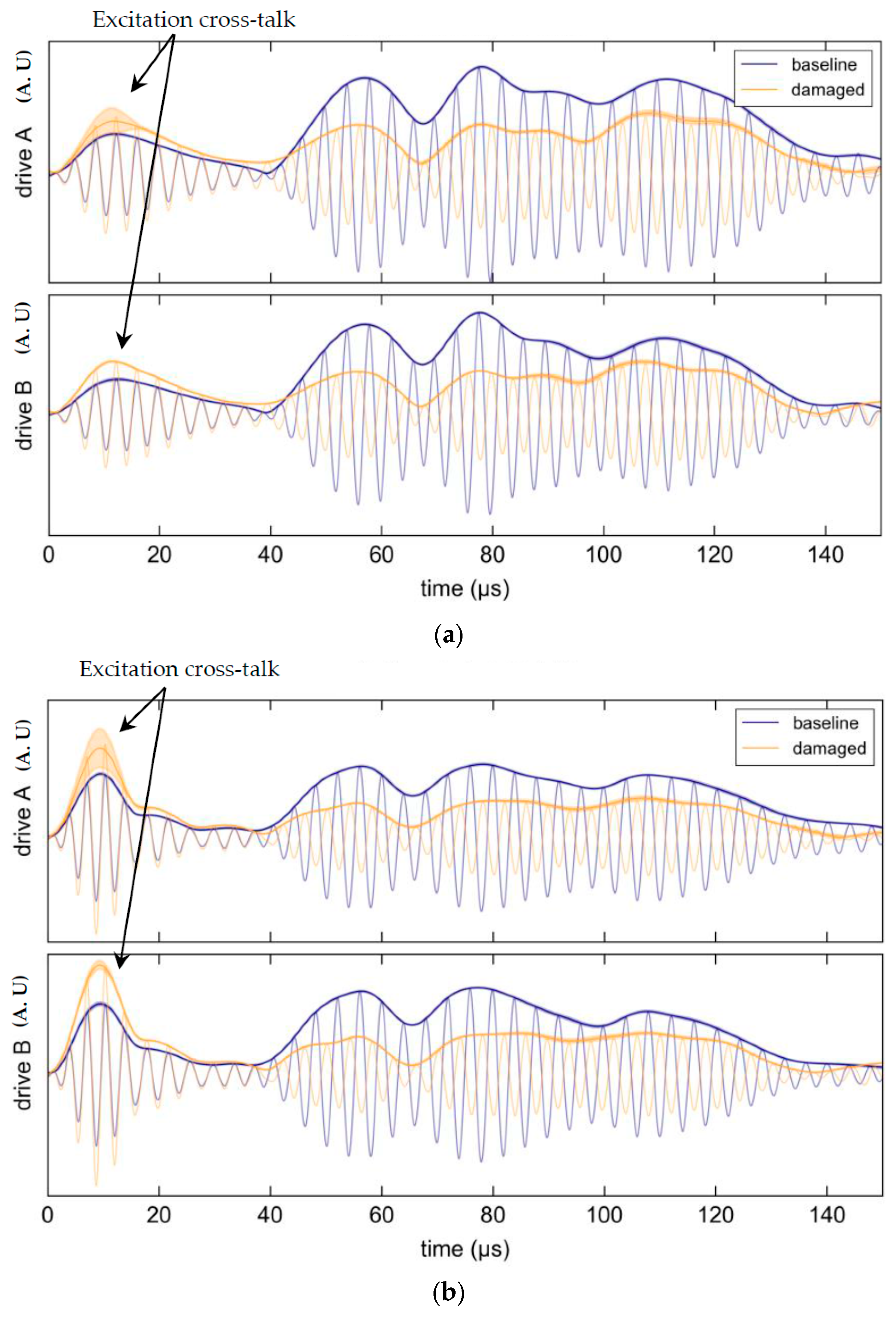
Figure 36.
Waveforms for pitch-catch interrogation in both directions; top plots show excitation on PWAS channel A and bottom plot shows excitation on PWAS channel B. The Hilbert transform envelopes are displayed and any shading represents two standard deviations in variability over 10 consecutive sweeps: (a) 250 KHz; (b) 300 KHz; (c) 350 KHz; (d) 400 KHz.
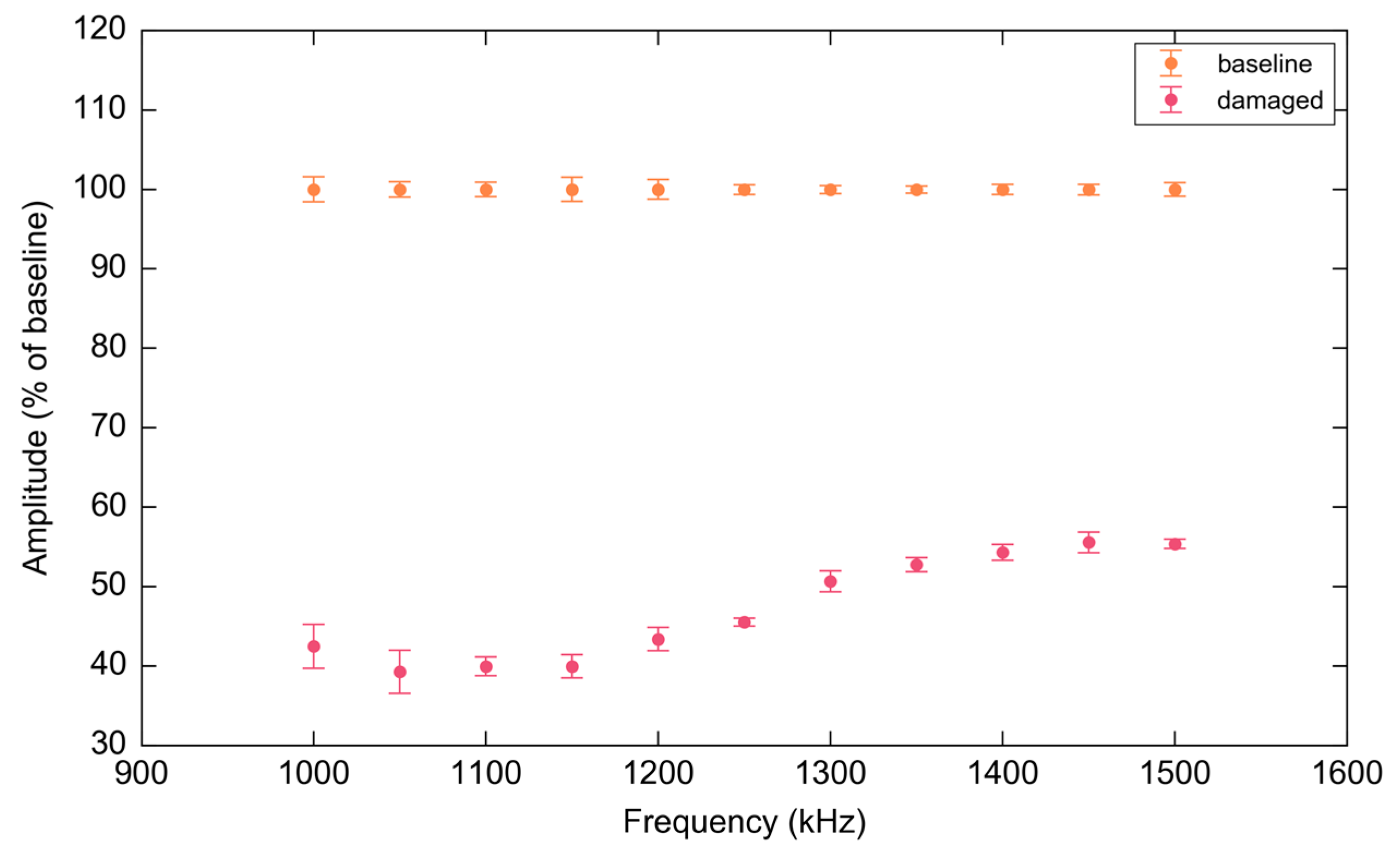
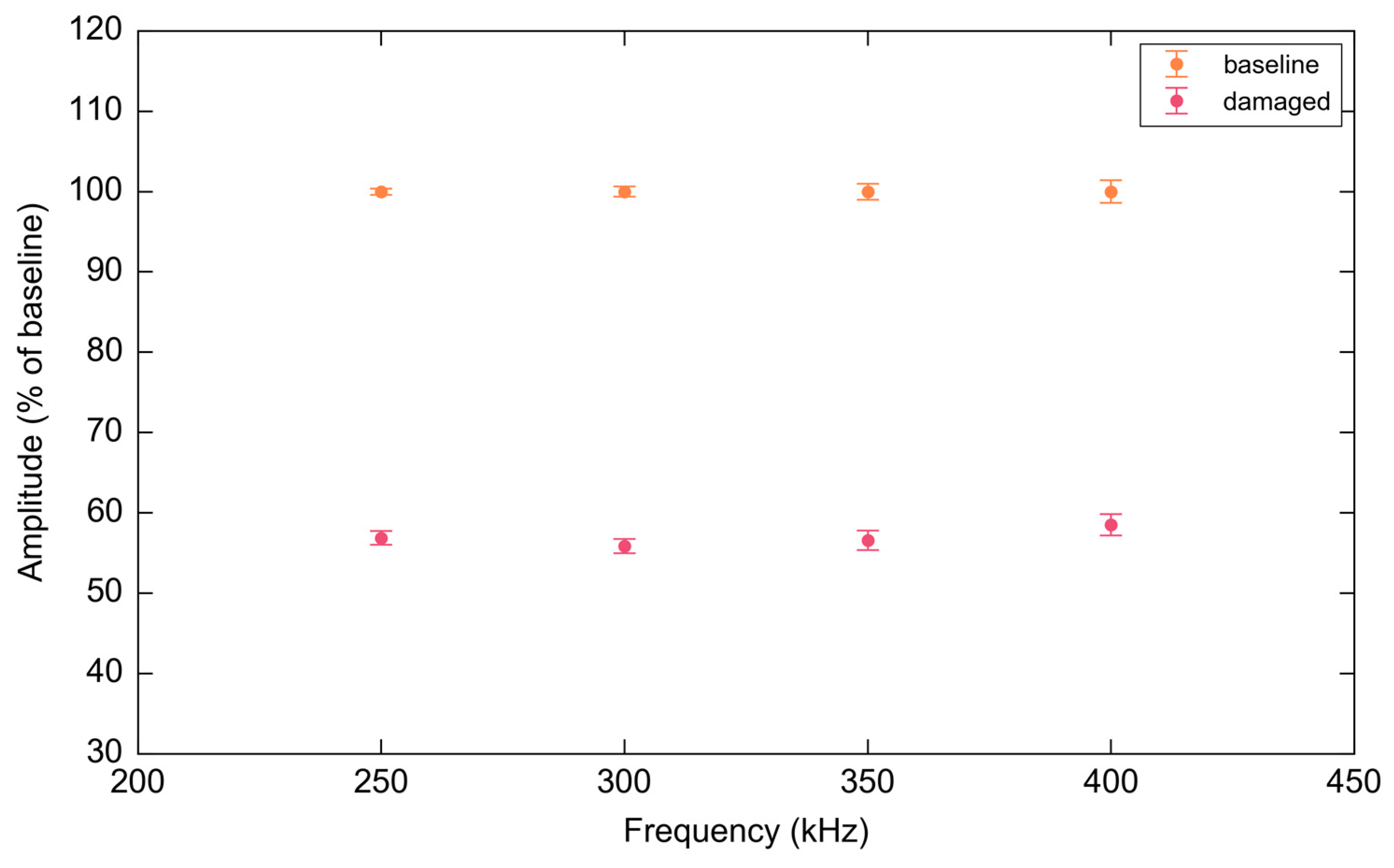
Figure 37.
Attenuation due to coupon damage as a normalized percentage of the baseline calculated using a Riemann sum of the signal envelope in the time window 40–150 μs. Error bars represent two standard deviations showing the variability over ten consecutive sweeps.
Figure 37.
Attenuation due to coupon damage as a normalized percentage of the baseline calculated using a Riemann sum of the signal envelope in the time window 40–150 μs. Error bars represent two standard deviations showing the variability over ten consecutive sweeps.
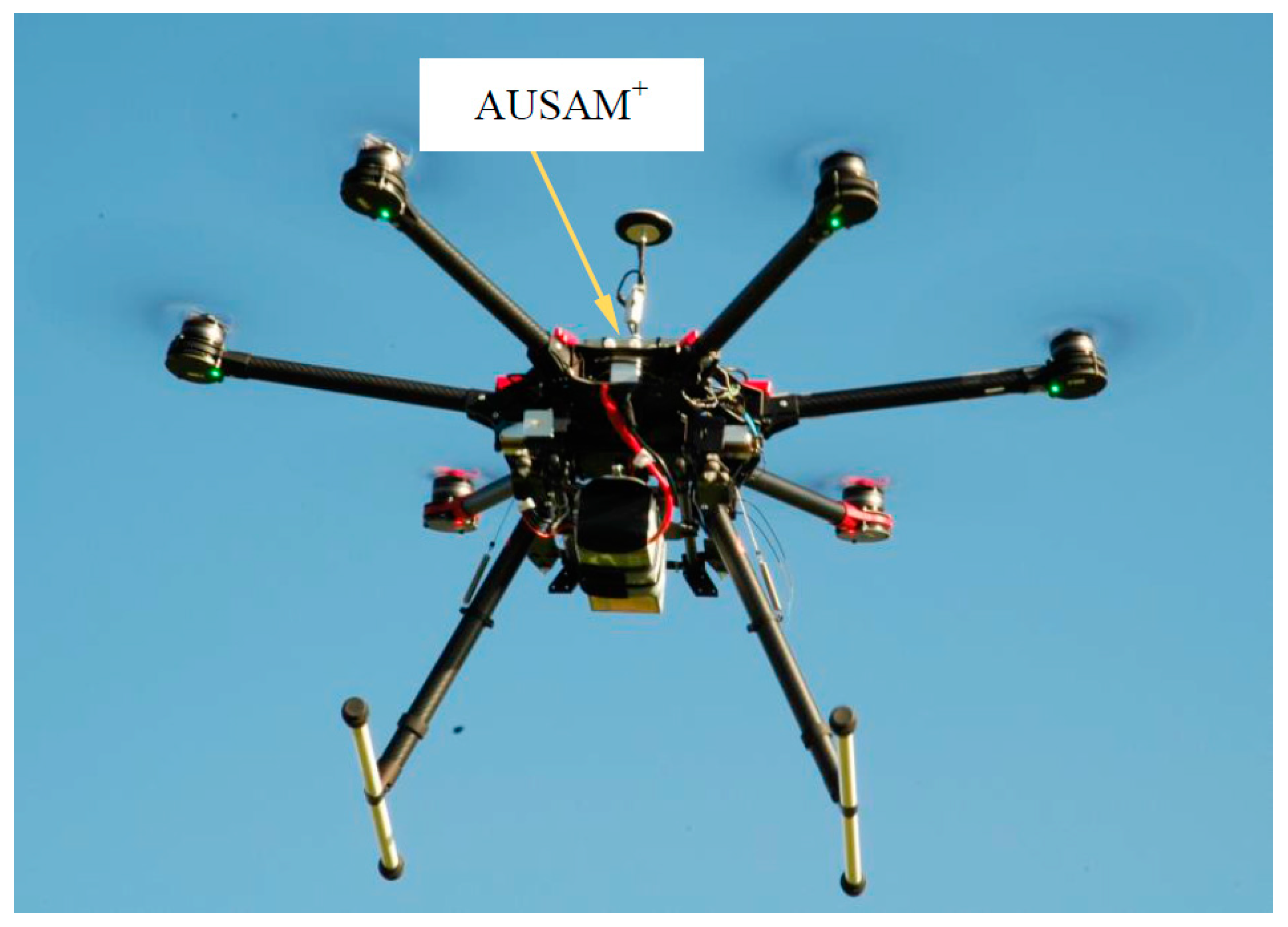
Figure 38.
AUSAM+ strapped on-board a SJ900 Hexacopter during flight testing.
Figure 38.
AUSAM+ strapped on-board a SJ900 Hexacopter during flight testing.
Table 1.
AUSAM+ acquisition system AFE channel configurations when Drive Monitoring is selected.
Table 1.
AUSAM+ acquisition system AFE channel configurations when Drive Monitoring is selected.
| HVDA Excitation Channel | Voltage Measurement Channel | Current Measurement Channel | Configuration State (All PIN Photodiode Opt Buffer Amplifiers = Disabled) |
|---|
| Channel A or Channel B | Channel D | Channel C | Channel D Voltage Monitor switch = ON
Channel D TRS = OFF
Channel C TRS = OFF
Channel C Current Amplifier = Enabled
Channel B Current Amplifier = Disabled |
| Channel C or Channel D | Channel A | Channel B | Channel A Voltage Monitor switch = ON
Channel A TRS = OFF
Channel B TRS = OFF
Channel B Current Amplifier = Enabled
Channel C Current Amplifier = Disabled |
Table 2.
Location of PWAS elements on rectangular panel.
Table 2.
Location of PWAS elements on rectangular panel.
| PWAS | 1 | 2 | 3 | 4 | 5 | 6 | 7 | 8 | 9 | 10 | 11 |
|---|
| x (mm) | 100 | 100 | 100 | 100 | 100 | 450 | 450 | 450 | 800 | 800 | 800 |
| y (mm) | 100 | 175 | 250 | 325 | 400 | 100 | 250 | 400 | 100 | 250 | 400 |

 ,
, 


