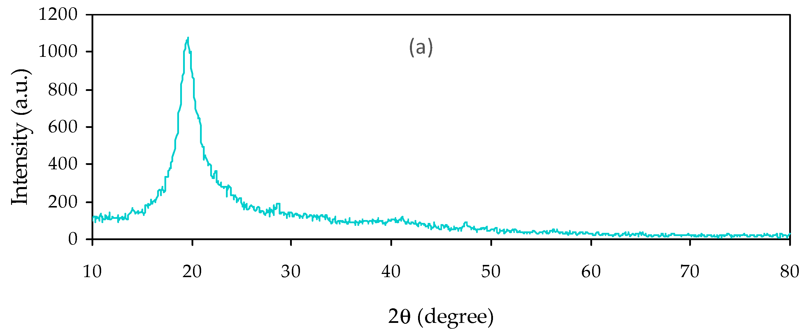
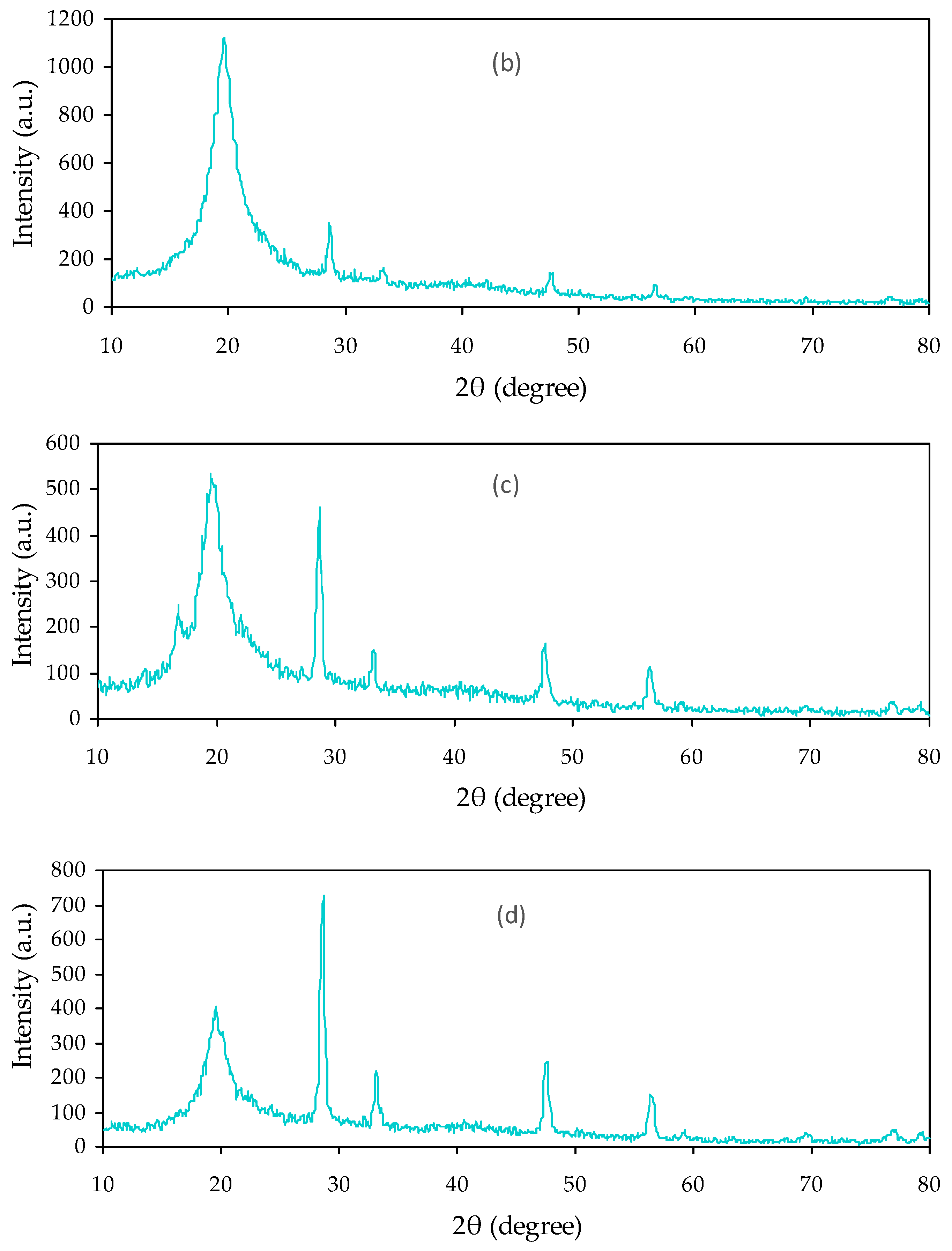
3.2.1. Absorption Study
Dealing with optical properties and recognizing electronic transitions within polymer NC films can be carried out using ultraviolet–visible (UV–Vis) spectroscopy. The optical absorption can be increased upon the addition of CeO
2 filler into PVA samples, as shown in
Figure 3. This can be interconnected to hosting new electronic levels into the prohibited gap within the PVA polymer [
8,
34,
35]; thereby, the wide BG of PVA can be narrowed. The influence of CeO
2 filler on the pure PVA can be confirmed from the shifting of the peak in the UV–Vis Spectra short toward longer wavelengths for all polymer samples encompassing CeO
2 filler. A considerable absorption occurs at high wavelengths, as exhibited in
Figure 3. It was also noticed that the absorption occupied a wide range of the spectra, suggesting the eligibility of these samples as raw materials for utilization in optoelectronic devices. The stronger exponential performance of the absorption vs. wavelength is evidenced for the NCPs films, compared to pure PVA.
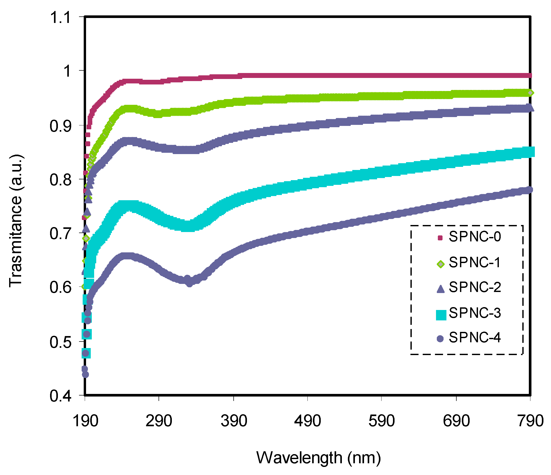
Figure 4 displays the transmittance of pure and doped PVA samples with varying amounts of CeO
2. The pure PVA had a relatively high degree of transparency beyond the visible region, over 97%, although the transparency decreased below the visible region due to the high absorption of the films. The transparency lowered and reached almost 74% for the doped PVA with CeO
2 at 7%. This transparency drop aroused from relatively high refractive index and significant scattering of films at high CeO
2 content. In the doped films, the spectrum possesses a shoulder, while in the pure PVA, a weak intensity shoulder can be seen. This suggests that the functional groups inside the polymer chains interact strongly with the added CeO
2 fillers, causing the doped films’ transparency to decrease.
Identifying the type of electron transitions in materials can be determined from the alterations in absorption spectra. Band-to-band transitions are associated with fundamental absorption, taking the form of a fast rise in absorption called the absorption edge. This edge is a measure of the optical BG energy [
36,
37]. The extent of absorption is based on an absorption coefficient
α (
υ), indicating the relative rate at which the incident light intensity attenuates in a unit length of the medium [
11,
38,
39]. Determination of the (
υ) at the equivalent frequency (υ) from the absorbance spectra
A(
υ) can be performed using Beer–Lambert law [
6,
36,
37]:
where the incident light and transmitted light intensities are denoted by
Io and
I, respectively, and the sample thickness is represented by
d. Figure 5 shows
α(
υ) against photon energy (
hυ) for pure PVA and PVA films doped with CeO
2 samples. The absorption edge values can be calculated by extrapolating the linear part to zero of the ordinate. Upon the addition of CeO
2 NPs, the absorption edge was found to shift to the direction of low photon energy, from 6.38 eV to 6 eV for pure PVA and PVA NC samples. Alteration in the sample band structure points out from the drop in the absorption edge value as CeO
2 added, resulting from the establishment of fresh localized states in the mobility gap [
40]. The absorption edge values of the pure and CeO
2 nanofiller-doped samples are tabulated in
Table 3.
3.2.2. Complex Optical Dielectric Constant ( and ) and Refractive Index (n) Study
Figure 6 indicates the
n of PVA with varying concentrations of CeO
2 fillers. From the absorbance (A) and reflectance (R) spectra, several optical parameters of the samples can be derived. The optical
n, which measures the light speed’s reduction rate through a medium, is essential among these parameters [
41]. For the calculation of the sample refractive index value, the reflectance (
R) and extinction coefficient (
K) are taken into account; the following equation is applied [
42]:
The increment in CeO
2 NPs is contributing to an increase in the refractive index. It is shown that a broad dispersion region and a high refractive index over a wide spectrum of wavelengths characterize the samples. The high
n polymers have recently been used for several applications, such as display devices, advanced organic light-emitting diodes (OLEDs), anti-refractive coatings, and various semiconductors [
43,
44]. Based on this impressive property, numerous researchers have focused on increasing the
n of polymers. Numerous methodologies have been implemented, for instance, incorporation of perfluorocyclobutane group, adamantane group, and sulfur atom into polymers and organic/inorganic DPs [
45,
46]. The refractive index is the essential property of those materials utilized in optoelectronic and photonic devices.
One such in particular are organic solar cells (OSCs). Thus, a deep understanding of this property is of great importance to evaluate efficient solar cells [
47]. It is well-known that a high refractive index is requested for organic solar cells at a large scale [
48,
49,
50,
51]. In the present work, the obtained refractive index for PVA by ion incorporation is relatively higher than reported throughout the literature [
49]. The broad dispersion of
n for PVA by ion incorporation is more significant than that reported by Shi et al. for nonlinear optical (NLO) polymers, polyetherketone (PEK-c) [
50]. This is a vital material for the large-scale applications of integrated-optic devices, such as electro-optic modulators and switches. The refractive index for a variety of polymer composites is presented in
Table 4.
The complex optical dielectric constant consisting of real (
) and imaginary (
) parts has also been acquired. Several parameters can be derived from this spectrum, closely associated with the energy state density within the samples’ optical BG [
55,
56]. It should be noted that the dielectric function cannot be measured from optical spectroscopy, directly. However, direct functions, such as the R, A,
n, and extinction coefficient (
K), can be accessed.
Figure 7 shows the
εr of the PVA-based NCPs samples. The dielectric function (DF) largely relies on the materials’ band structure. The analysis of DF using optical spectroscopy has been established to be informative in imagining the materials’ overall band structure [
57,
58]. It is shown from
Figure 7 that the
εr increases with the quantity of CeO
2 NPs are increasing. This rise in dielectric constant suggests that the energy density of states is comparatively high. This also results in a polarization boost, which gives a relatively high dielectric constant value. The optical
εr is seen as a dispersion region at low wavelengths, while the values are almost constant at high wavelengths.
Due to exposure to an incident electromagnetic light, materials’ internal charge structure undergoes a time-varying force. This is owing to the influence of the electric field component of the incident wave. The broad dispersion region is correlated with the polar nature of the samples. It is worth noting that, due to its inertia at high wavelengths, polar molecules cannot obey the field alternation [
59]. The dispersion in dielectric constant shows that these materials can be qualified for industrial use, particularly in designing optical devices and the optical communication field [
60,
61,
62].
3.2.3. Bandgap Study
It is well-known that optical properties and the electronic band structure are closely correlated [
13,
63,
64]. One of the characteristics of absorbing isotropic materials is the complex optical DF dependence on the wavelength (
λ) [
65]. The decisive optical functions can be determined from both the real and imaginary parts of the DF [
66]. More precisely, the electronic polarizability and the electronic absorption can be determined from the
εr(ω) and the
εi(ω), correspondingly [
67].
The direct and indirect BG transitions are both related to the ε
(ω), while direct transitions are more involved in the
ε(ω), in comparison to the indirect transitions, as a consequence of mediation by phonons in the latter one [
64]. It was previously verified that it is difficult to accurately determine the optical BG from the KT and Taucs equations from certain disposable constants in formulas [
68,
69,
70,
71]. However, a simple and effective technique has been established with sufficient accuracy to analyze the optical BG [
6,
13,
70]. The desired technique to determine the optical BG precisely is data analysis of optical dielectric loss. Such a technique is established on the modern improvements in quantum mechanics and numerous models. Based on quantum mechanics, the time-dependent perturbations of ground electronic state are the foundation in the photon–electron interaction characterization inside a system. The photon absorption and emission are causes of the alteration from full to vacant states. The dielectric function’s imaginary part ε
i(ω) has the following form [
6]:
where
u and
k are the vectors that characterize the incident electric field polarization and the reciprocal lattice, respectively. The superscripts
C and
V signify the conduction and the valence bands, respectively, and
ω symbolizes the incident photon frequency [
72].
Figure 8 displays the imaginary part of the dielectric constant
εi(ω) spectra. From the joint of linear parts on the
x-axis, one can determine the optical BG. It is important to note that the optical spectra result from the top of full bands to the lowest of conduction bands. The fundamental absorption edge, also referred to as the basic absorption edge, is the most distinctive optical BG feature [
73]. It is noted that the significant points are closely correlated with the values of the BG [
74].
Table 5 shows the BG values obtained from dielectric loss spectra. Both the energy BG and the refractive index of CeO
2 NPs do not reflect the same effect. The optical properties, i.e., refractive index and energy gap, have been reported to be closely interrelated to the variation in material compositions and atomic configurations [
75]. Within the pure PVA BG, the formation of localized states, i.e., rising density state, effectively decreases the BG energy. The high refractive index of the samples, in other words, means the high density of state. From the renowned Clausius–Mossotti relation, the refractive index’s reliance on film density can be rationalized [
57].
The type of electronic transition inside the material BG can be recognized using the interband absorption model. A photon can excite an electron from a top, occupied valence band to a bottom, unoccupied conduction band. There is a mathematical relationship based on this model, from which the material’s optical BG can be determined [
76,
77]:
where
B and
Eg, respectively, signify the energy-independent constant and optical energy BG. The constant
p specifies the nature of the optical transition from the valence- to conduction-band, i.e., fundamental absorption.
According to the selection rule, when
p = 1/2, it indicates the allowance of direct transition. The electron vertically transfers from the top valence band to the bottom conduction band during the direct allowance transition. On the other hand, the nonvertical transitions are usually known as indirect allowed transitions, and
p takes a value of 2 in this case [
76]. It should also be noted that
p takes 3 and 3/2 values for indirect and direct forbidden transitions, respectively. Based on the Taucs model, the different kinds of electronic transitions between the valence band (VB) and conduction band (CB) can be shown in
Figure 9 [
59].
The dependence of
versus
of pure PVA and PVA-doped samples are exhibited in
Figure 10. The direct energy gaps of all the samples are presented in
Table 5. The optical energy gap values can be obtained from extrapolation of the linear part of the plot to zero absorption. From
Table 5, one can note that the values of the optical bandgaps calculated from dielectric study are close to those obtained from Tauc’s relation, where (
p = 1/2). This outcome reveals that the prepared samples exhibi the direct allowed transition, which means that the samples are having direct optical BG.
It should be noticed that the energy BG of pure PVA, in comparison with other samples, is relatively large (5.38 eV). In the present work, the pure PVA’s obtained direct optical BG is well-matched by the literature [
78]. Based on solid-state physics principles, the energy BG in a solid is a range of energy where no electron states exist. The energy required to free a bound electron from the outermost shell to become a conductive electron within the materials is the energy BG. Furthermore, in terms of electrical conductivity, the BG energy is considered the main barrier in solid materials. Materials with small and large BG are known as insulator and semiconductor materials, respectively. In this regard, the pure PVA is a pure insulator, since its BG is 5.36 eV large, suggesting the lack of free carrier absorption. In PVA, the only existing band is the interband transitions that becoming interesting material with relatively high photon energy, as shown in
Figure 8a.
In the present work, the BG of PVA can be changed to be eligible for a specific application via the addition of an optimum portion of the tea solution. It has been emphasized that the narrow BG materials are considered as the desired candidate materials to compensate for the low energy photon harvest [
79]. Thus, the process of lowering the BG energy of PVA polymer via the incorporation of environmentally friendly tea materials can be regarded as a breakthrough in optical materials. It also makes a new revolution in organic solar cells and optoelectronic devices.
Close the ultimate band edge, the direct and indirect transitions will occur and can be shown by plotting (
αhυ)
1/2 and (
αhυ)
2, dependent on photon energy (
hυ) [
80,
81].
Figure 10,
Figure 11 and
Figure 12 demonstrate the plot of (
αhυ) versus photon energy (
hυ) for each exponent (
n) value in the Tauc’s equation. In these plots, linear parts can be seen, and the BG energies can be determined from the intersections of the
x-axis. Amorphous materials’ absorption edge can be evaluated from the indirectly allowed transitions, depending on their electronic configuration [
82]. Thus, in the case of amorphous materials, indirect transitions should be taken into account.
On the other hand, in the indirect BG materials, the electron transition from the valence to conduction bands correlates with a phonon of right crystal momentum magnitude [
80]. Since the acquired optical BG values differ according to the exponent (
n), choosing (
n) value can be principally impossible. Therefore, based on Equation (4), the type of conduction mechanism can be rationalized. In the meanwhile, an additional parameter, namely the dielectric constant from the imaginary part (
ε2), is used to calculate the actual
Eopt; thereby, the exact exponent value can be chosen [
82].
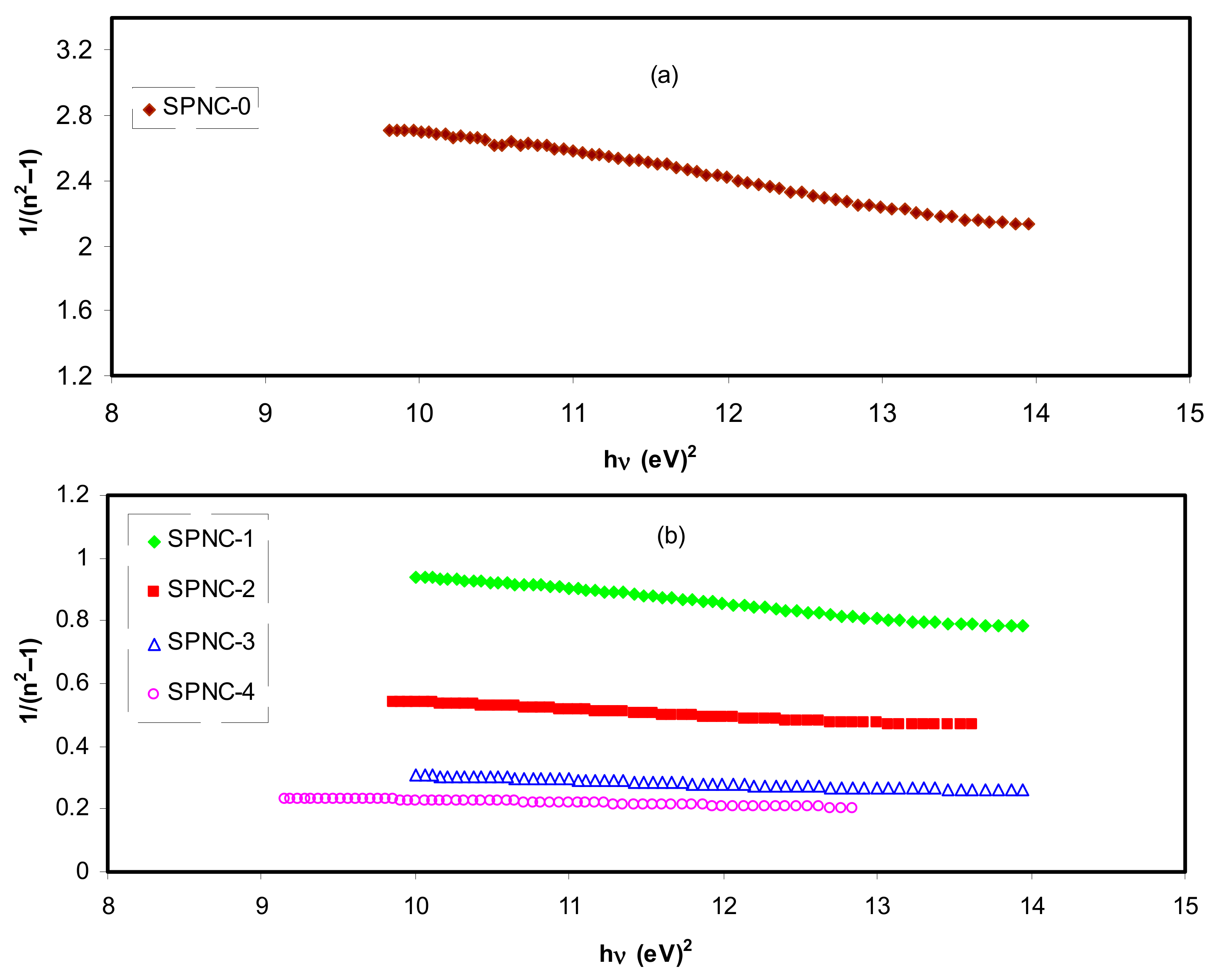
3.2.4. Wemple–DiDomenico (W–D) Model
Refractive index and its dispersion manners are among the decisive properties of the optical materials. Particularly, the refractive index dispersion is found to be very significant for optical communication and in designing devices for spectral dispersion [
83]. The refractive index dispersion in the normal region can be explored using the well-known single oscillator model presented by W–D [
84,
85]. The investigation is usually done by introducing a dispersion energy parameter (
Ed) as a gauge of the force of interband optical transition. Both the coordination number with the charge allocation in each unit cell are combined through the
Ed parameter, which is strongly interrelated to the chemical bonding [
86,
87]. Nevertheless, a single oscillator parameter (
Eo) is proportional to the energy of oscillator (average energy bandgap). Using a semiempirical equation (Equation (6)), both photon energy and refractive index under the interband absorption edge can be correlated as follows:
As portrayed in
Figure 13, the data on the plots of
against
(hυ)2 were fitted with linear regression lines to acquire the values of
Ed and
Eo from the intercept and slope, correspondingly. The calculated values of the
Eo and
Ed are presented in
Table 6. A raise in
Ed (see
Table 5) is observed, which characterizes the increase of average strength of interband optical transitions. The
no value achieved from the W–D model is sufficiently close to
n values shown in
Figure 6 at high wavelengths. For the present films, empirically the
Eo values are near to the
Eg values presented in
Table 5. Hence, the from W–D model, it is achievable to get the
Eg and (
values for the films; however, it is still hard to identify the type of transition from VB to CB.


 ,
, 


