
Grain Size Effects on Mechanical Properties of Nanocrystalline Cu6Sn5 Investigated Using Molecular Dynamics Simulation

Abstract
:1. Introduction
2. Methodology
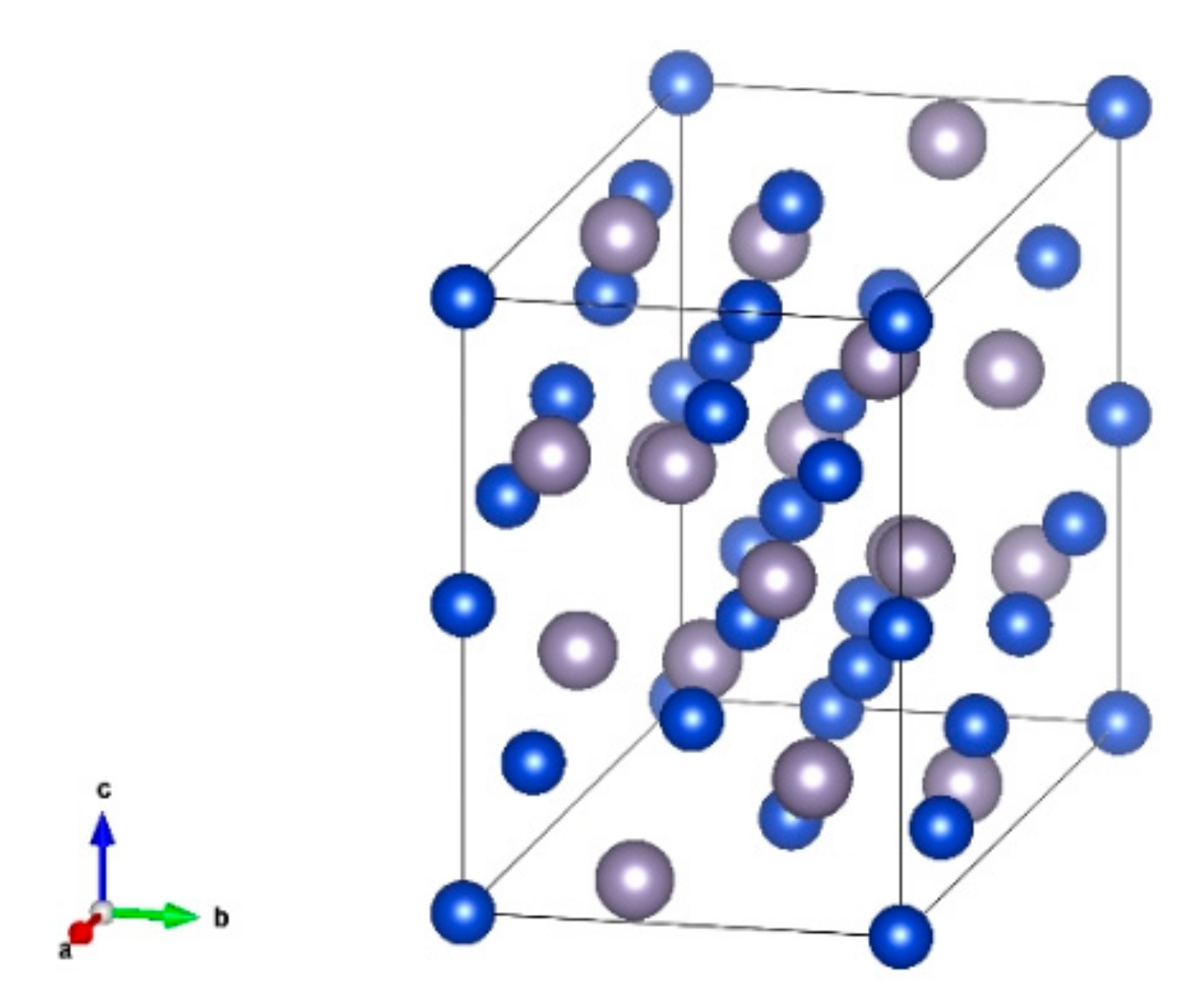
2.1. MEAM Potential
2.2. Establishment of Polycrystals
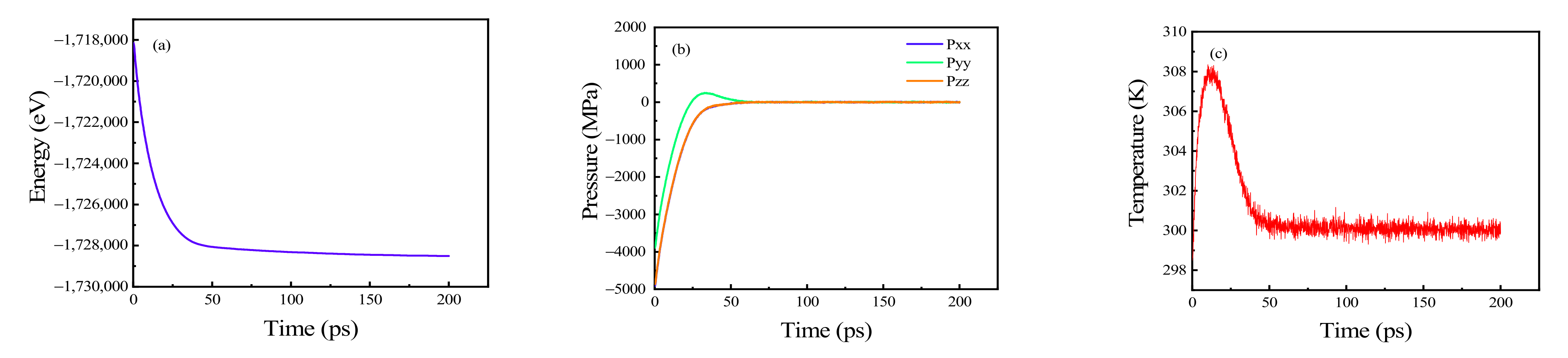
2.3. Simulation Settings
3. Results and Discussion
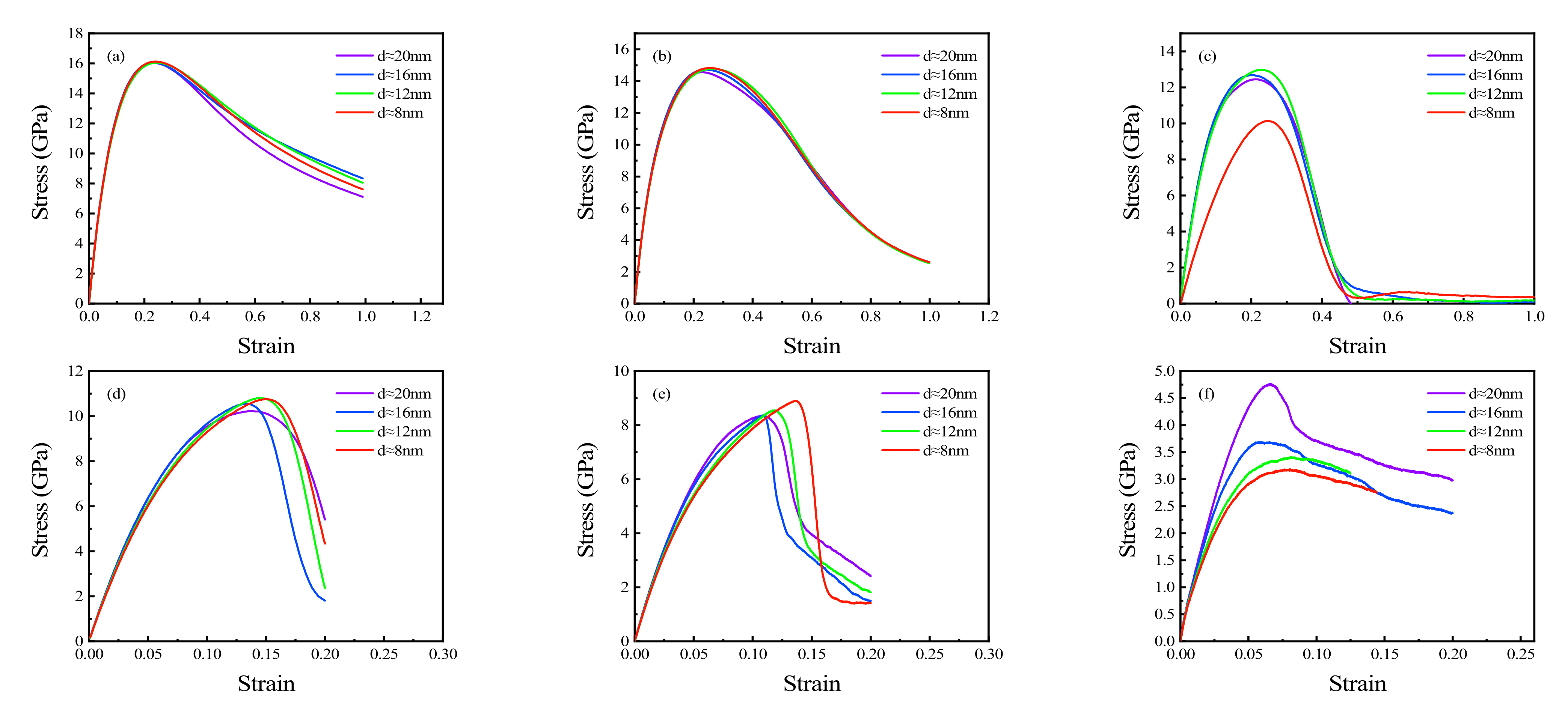
3.1. Stress-Strain Responses at Different Strain Rates
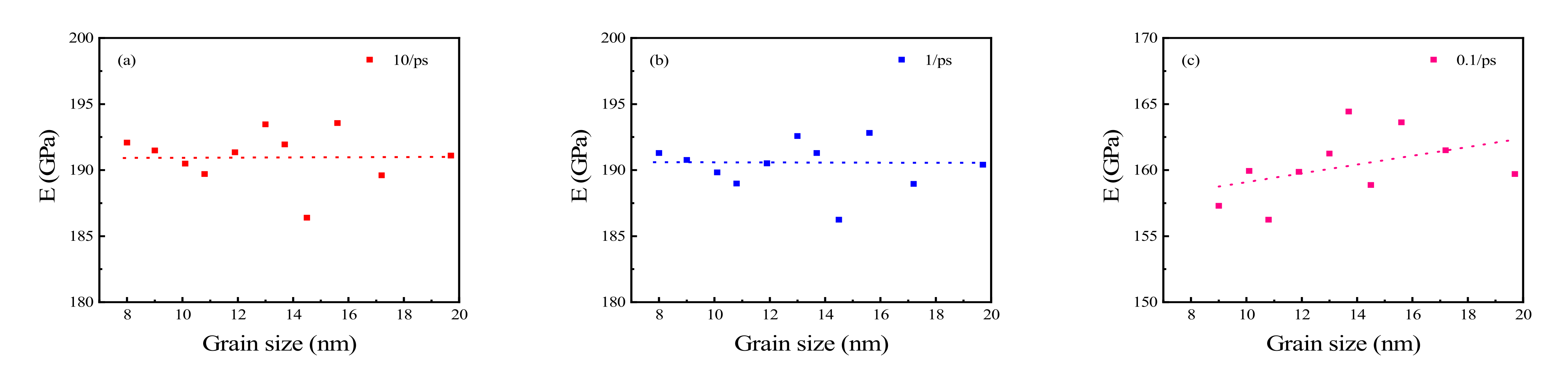
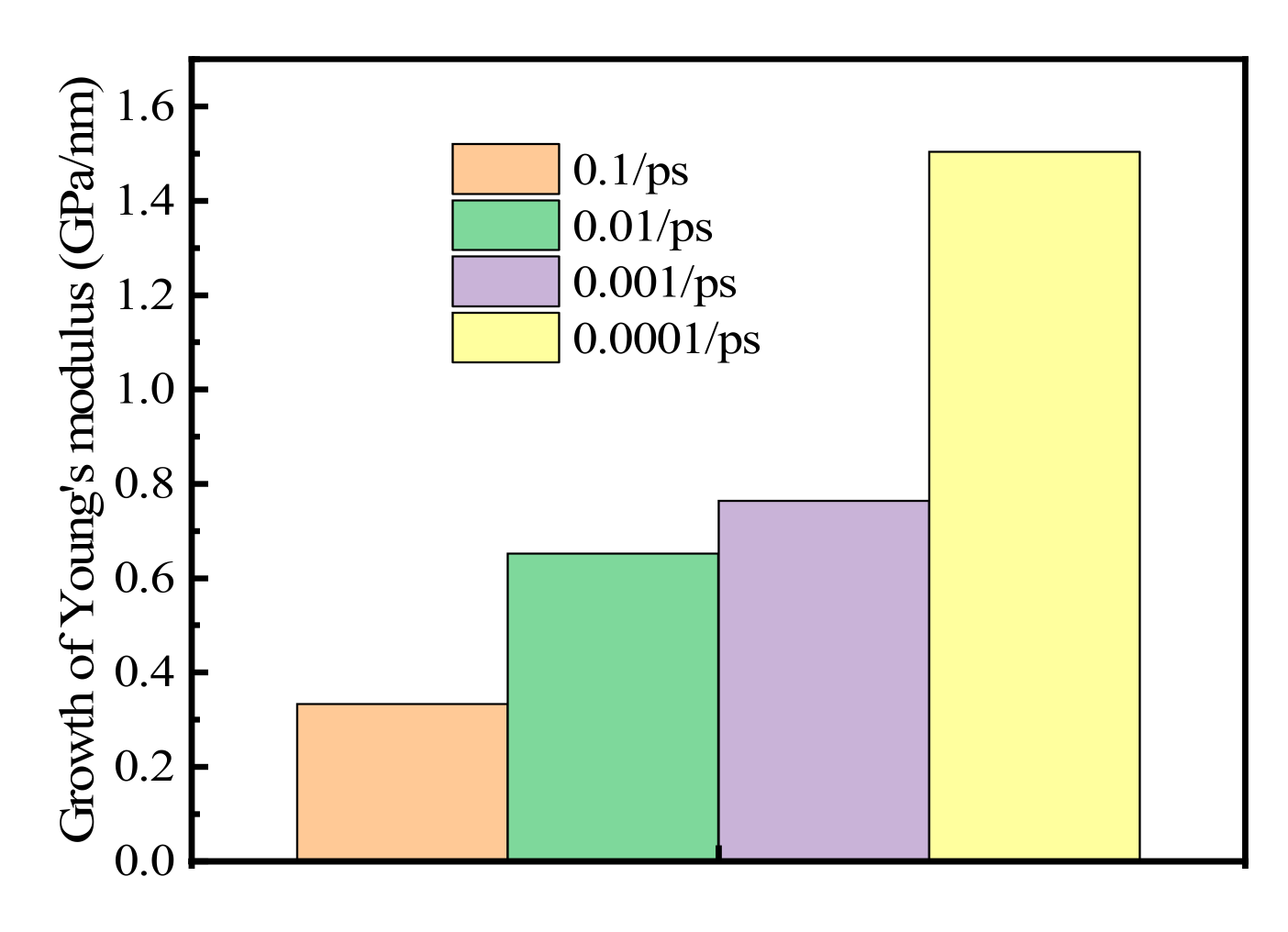
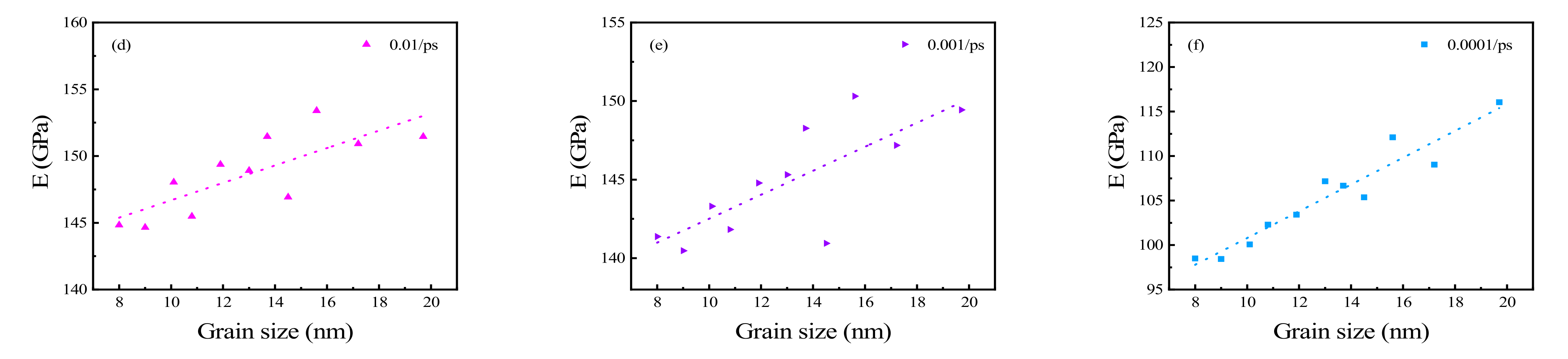
3.2. Elastic Properties of Polycrystalline Cu6Sn5
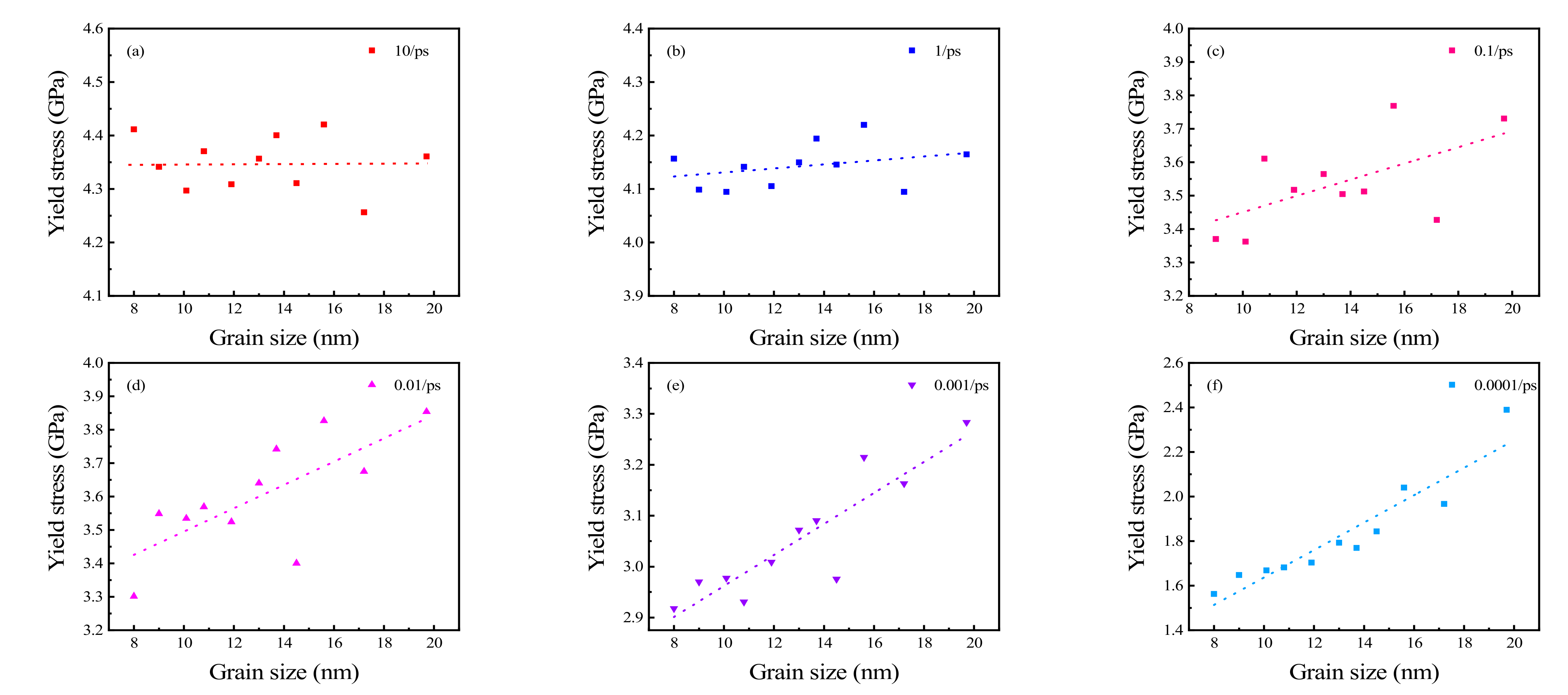
3.3. Yield Stress of Polycrystalline Cu6Sn5 with Different Grain Sizes
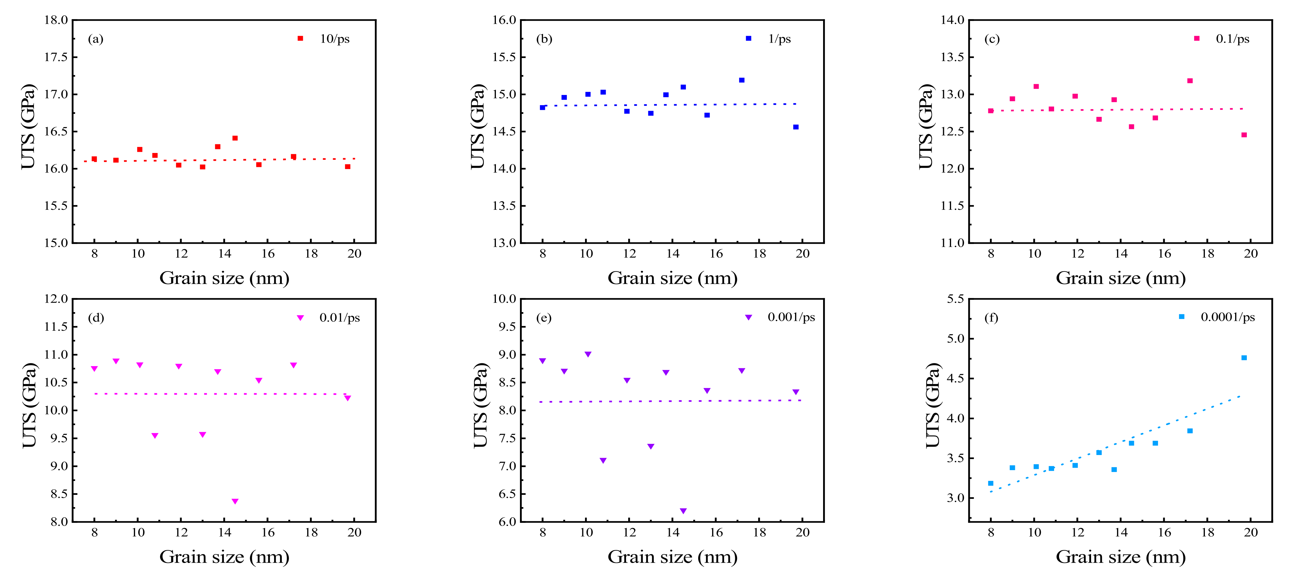
3.4. Grain Size Effects on UTS of Polycrystalline Cu6Sn5
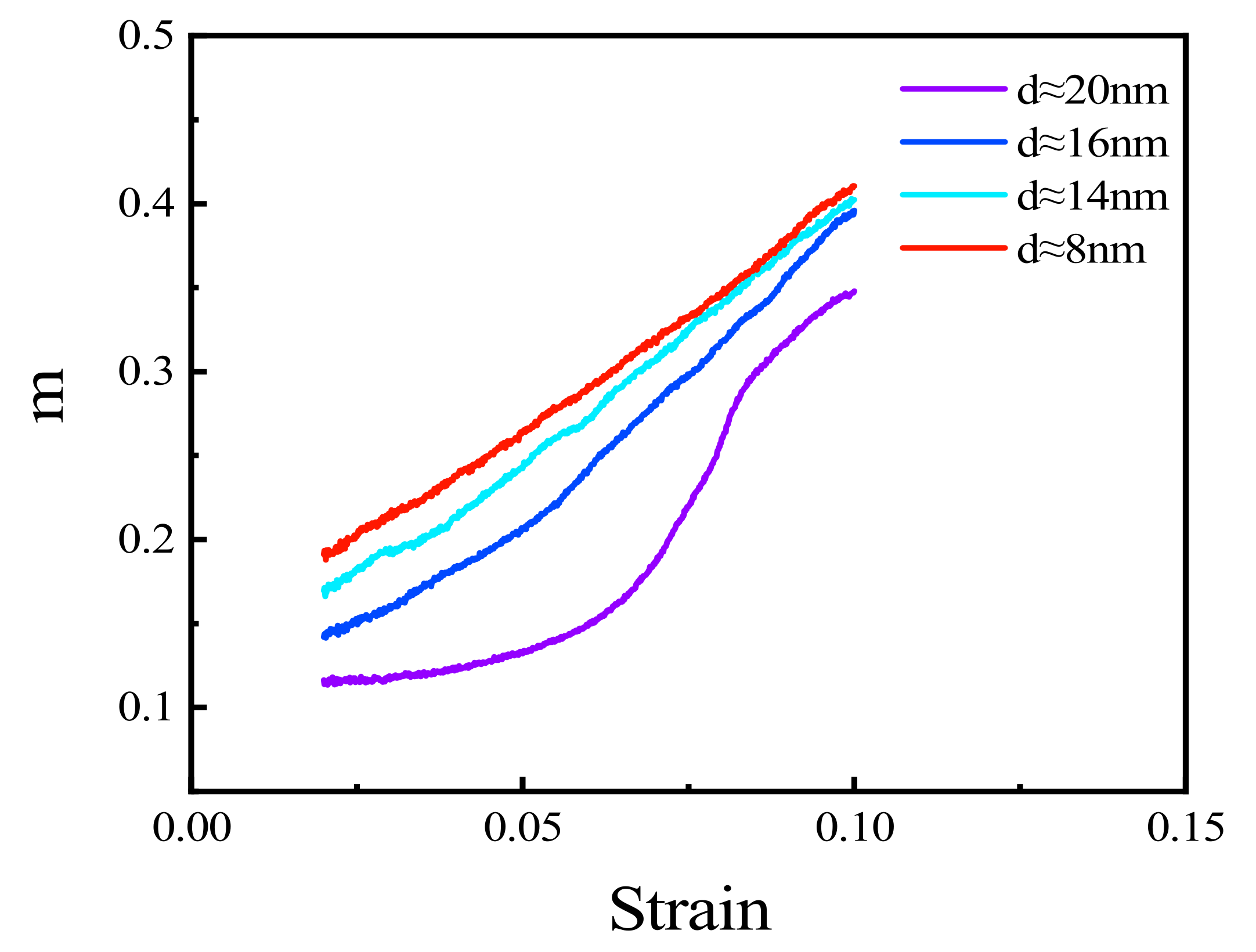
3.5. Strain Rate Sensitivity of Polycrystalline Cu6Sn5
4. Conclusions
- The effect of grain size on the stress-strain curve increases with decreasing strain rate and is practically invisible at high strain. This conclusion can be particularised for Young modulus, yield stress, and UTS.
- Young’s modulus, yield stress, and UTS increase with the increasing grain size at a lower strain rate. Moreover, the growth rate of the Young’s modulus increases with a decrease in strain rate.
- Polycrystals with a small grain size are more sensitive to strain rate than those with a large grain size. The strain rate sensitivity of polycrystalline Cu6Sn5 increases with increasing strain rate.
Author Contributions
Funding
Institutional Review Board Statement
Informed Consent Statement
Data Availability Statement
Conflicts of Interest
References
- Xiong, M.-y.; Zhang, L. Interface reaction and intermetallic compound growth behavior of Sn-Ag-Cu lead-free solder joints on different substrates in electronic packaging. J. Mater. Sci. 2018, 54, 1741–1768. [Google Scholar] [CrossRef]
- Qiu, H.; Hu, X.; Li, S.; Wan, Y.; Li, Q. Shear strength and fracture surface analysis of lead-free solder joints with high fraction of IMCs. Vacuum 2020, 180, 109611. [Google Scholar] [CrossRef]
- Zhao, M.; Zhang, L.; Liu, Z.Q.; Xiong, M.Y.; Sun, L. Structure and properties of Sn-Cu lead-free solders in electronics packaging. Sci. Technol. Adv. Mater. 2019, 20, 421–444. [Google Scholar] [CrossRef] [Green Version]
- Marques, V.M.F.; Johnston, C.; Grant, P.S. Nanomechanical characterization of Sn–Ag–Cu/Cu joints—Part 1: Young’s modulus, hardness and deformation mechanisms as a function of temperature. Acta Mater. 2013, 61, 2460–2470. [Google Scholar] [CrossRef]
- Chen, Z.; Liu, C.; An, B.; Wu, Y.; Liu, L. Evolution of the hardness and Young’s moduli of interlayers in Sn99Cu1/Cu solder joints subjected to isothermal ageing. J. Mater. Sci. Mater. Electron. 2017, 28, 17461–17467. [Google Scholar] [CrossRef]
- Yin, Z.; Sun, F.; Guo, M. Investigation of elevated temperature mechanical properties of intermetallic compounds in the Cu-Sn system using nanoindentation. J. Electron. Packaging 2020, 142, 021004. [Google Scholar] [CrossRef]
- Zhang, A.Q.; Peng, P.; Zheng, W.C.; Yang, J.R.; Zhang, X.D.; Xu, Y.L. Phase selection and nano-mechanical properties of intermetallic compounds in directionally solidified Cu-68at.%Sn peritectic alloy. J. Alloys Compds. 2021, 859, 157866. [Google Scholar] [CrossRef]
- Haseeb, A.S.M.A.; Rahman, A.Z.M.S.; Chia, P.Y. Nanoindentation creep on Cu3Sn, Cu6Sn5 and (Cu, Ni)(6)Sn-5 intermetallic compounds grown in electrodeposited multilayered thin film. J. Mater. Sci. Mater. Electron. 2018, 29, 1258–1263. [Google Scholar] [CrossRef]
- Feng, J.; Hang, C.; Tian, Y.; Wang, C.; Liu, B. Effect of electric current on grain orientation and mechanical properties of Cu-Sn intermetallic compounds joints. J. Alloys Compds. 2018, 753, 203–211. [Google Scholar] [CrossRef]
- Rahman, A.Z.M.S.; Chia, P.Y.; Haseeb, A.S.M.A. Mechanical properties of intermetallic compounds in electrodeposited multilayered thin film at small scale by nanoindentation. Mater. Lett. 2015, 147, 50–53. [Google Scholar] [CrossRef]
- Mo, L.; Chen, Z.; Wu, F.; Liu, C. Microstructural and mechanical analysis on cu-sn intermetallic micro-joints under isothermal condition. Intermetallics 2015, 66, 13–21. [Google Scholar] [CrossRef] [Green Version]
- Zhang, W.W.; Ma, Y.; Zhou, W.; Wu, P. The structural, elastic and electronic properties of ni3−xcuxsn4 (x = 0, 0.5, 1 and 1.5) intermetallic compounds via ab initio calculations. J. Electron. Mater. 2019, 48, 4533–4543. [Google Scholar] [CrossRef]
- Bi, X.; Hu, X.; Jiang, X.; Li, Q. Effect of Cu additions on mechanical properties of ni3sn4-based intermetallic compounds: First-principles calculations and nano-indentation measurements. Vacuum 2019, 164, 7–14. [Google Scholar] [CrossRef]
- Lee, N.T.S.; Tan, V.B.C.; Lim, K.M. First-principles calculations of structural and mechanical properties of Cu6Sn5. Appl. Phys. Lett. 2006, 88, 031913. [Google Scholar] [CrossRef]
- Ghosh, G.; Asta, M. Phase stability, phase transformations, and elastic properties of cu6sn5: Ab initio calculations and experimental results. J. Mater. Res. 2005, 20, 3102–3117. [Google Scholar] [CrossRef]
- Huang, W.; Pan, K.; Zhang, J.; Gong, Y. Effect of in-doping on mechanical properties of Cu6Sn5-based intermetallic compounds: A first-principles study. J. Electron. Mater. 2021, 50, 4164–4171. [Google Scholar] [CrossRef]
- Liang, L.; Zhang, J.; Xu, Y.; Zhang, Y.; Wang, W.; Yang, J. The effect of pressure and orientation on Cu-Cu3Sn Interface reliability under isothermal ageing and monotonic traction via molecular dynamics investigation. Mater. Des. 2018, 149, 194–204. [Google Scholar] [CrossRef]
- Cheng, H.-C.; Yu, C.-F.; Chen, W.-H. Size, temperature, and strain-rate dependence on tensile mechanical behaviors of ni3sn4 intermetallic compound using molecular dynamics simulation. J. Nanomater. 2014, 2014, 1–17. [Google Scholar] [CrossRef] [Green Version]
- Gao, F.; Qu, J. Calculating the diffusivity of Cu and Sn in Cu3Sn intermetallic by molecular dynamics simulations. Mater. Lett. 2012, 73, 92–94. [Google Scholar] [CrossRef]
- Huang, W.; Pan, K.; Zhang, J.; Gong, Y. Strain rate and temperature effects on tensile properties of polycrystalline Cu6Sn5 by molecular dynamic simulation. Crystals 2021, 11, 1415. [Google Scholar] [CrossRef]
- Motalab, M.; Paul, R.; Saha, S.; Mojumder, S.; Ahmed, T.; Suhling, J.C. Atomistic analysis of the thermomechanical properties of Sn-Ag-Cu solder materials at the nanoscale with the MEAM potential. J. Mol. Model. 2019, 25, 59. [Google Scholar] [CrossRef]
- Etesami, S.A.; Baskes, M.I.; Laradji, M.; Asadi, E. Thermodynamics of solid Sn and Pb Sn liquid mixtures using molecular dynamics simulations. Acta Mater. 2018, 161, 320–330. [Google Scholar] [CrossRef]
- Liu, B.-H.; Chen, Y.-L.; Hsu, Q.-C. Study on bonding and shear flow phenomena of shear probe test for BGA solder joint in nano-scale analysis. ASME 2016. [Google Scholar] [CrossRef]
- Hu, X.; Xu, T.; Keer, L.M.; Li, Y.; Jiang, X. Shear strength and fracture behavior of reflowed Sn3.0Ag0.5Cu/Cu solder joints under various strain rates. J. Alloys Compd. 2017, 690, 720–729. [Google Scholar] [CrossRef]
- Cheng, H.C.; Yu, C.F.; Chen, W.H. Strain- and strain-rate-dependent mechanical properties and behaviors of Cu3Sn compound using molecular dynamics simulation. J. Mater. Sci. 2012, 47, 3103–3114. [Google Scholar] [CrossRef]
- Yu, C.F.; Cheng, H.C.; Chen, W.H. Molecular Dynamics Calculations and Nanoindentation Testing of the Strain-Rate and Size Dependent Material Properties of Cu3Sn IMC. In Proceedings of the 2010 5th International Microsystems Packaging Assembly and Circuits Technology Conference, Taipei, Taiwan, 20–22 October 2010. [Google Scholar]
- Qin, F.; An, T.; Chen, N. Strain rate effects and rate-dependent constitutive models of lead-based and lead-free solders. J. Appl. Mech. 2010, 77, 011008. [Google Scholar] [CrossRef]
- Naik, S.N.; Walley, S.M. The Hall-Petch and inverse Hall-Petch relations and the hardness of nanocrystalline metals. J. Mater. Sci. 2020, 55, 2661–2681. [Google Scholar] [CrossRef] [Green Version]
- Zhou, X.-Y.; Zhu, J.-H.; Wu, H.-H. Molecular dynamics studies of the grain-size dependent hydrogen diffusion coefficient of nanograined Fe. Int. J. Hydr. Energy 2021, 46, 5842–5851. [Google Scholar] [CrossRef]
- Ma, Z.; Pathegama Gamage, R.; Zhang, C. Effects of temperature and grain size on the mechanical properties of polycrystalline quartz. Comput. Mater. Sci. 2021, 188, 110138. [Google Scholar] [CrossRef]
- Zhou, K.; Liu, B.; Yao, Y.; Zhong, K. Effects of grain size and shape on mechanical properties of nanocrystalline copper investigated by molecular dynamics. Mater. Sci. Eng. A 2014, 615, 92–97. [Google Scholar] [CrossRef]
- Alizadeh, J.; Salati, A.; Ebrahimi Fordoei, M.R.; Panjepour, M. Investigation of grain boundary influence on the thermodynamic phase stability of nanocrystalline iron by using the molecular dynamics simulation method. J. Mater. Eng. Perform. 2021, 30, 4681–4690. [Google Scholar] [CrossRef]
- Armstrong, R.W. Size effects on material yield strength/deformation/fracturing properties. J. Mater. Res. 2019, 34, 2161–2176. [Google Scholar] [CrossRef]
- Naughton-Duszova, A.; Csanadi, T.; Sedlak, R.; Hvizdos, P.; Dusza, J. Small-Scale Mechanical Testing of Cemented Carbides from the Micro- to the Nano-Level: A Review. Metals 2019, 9, 502. [Google Scholar] [CrossRef] [Green Version]
- Chen, W.-H.; Yu, C.-F.; Cheng, H.-C.; Lu, S.-T. Crystal size and direction dependence of the elastic properties of Cu3Sn through molecular dynamics simulation and nanoindentation testing. Microelectron. Reliab. 2012, 52, 1699–1710. [Google Scholar] [CrossRef]
- Plimpton, S. Fast parallel algorithms for short-range molecular-dynamics. J. Comp. Phys. 1995, 117, 1–19. [Google Scholar] [CrossRef] [Green Version]
- Baskes, M.I. Modified embedded-atom potentials for cubic materials and impurities. Phys. Rev. B Condens. Matter 1992, 46, 2727–2742. [Google Scholar] [CrossRef]
- Larsson, A.K. The superstructure of domain-twinned η’-Cu6Sn5. Acta Crystallogr. B 1994, 50, 636–643. [Google Scholar] [CrossRef]
- Aguilar, J.F.; Ravelo, R.; Baskes, M.I. Morphology and dynamics of 2D Sn-Cu alloys on (100) and (111) Cu surfaces. Model. Simul. Mater. Sci. Eng. 2000, 8, 335. [Google Scholar] [CrossRef]
- Hirel, P. Atomsk: A tool for manipulating and converting atomic data files. Comput. Phys. Commun. 2015, 197, 212–219. [Google Scholar] [CrossRef]
- Stukowski, A. Visualization and analysis of atomistic simulation data with OVITO–the open visualization tool. Model. Simul. Mater. Sci. Eng. 2010, 18, 2154–2162. [Google Scholar] [CrossRef]
- Hill, R. The elastic behaviour of a crystalline aggregate. Proc. Phys. Soc. A 1952, 65, 349–354. [Google Scholar] [CrossRef]
- Chokshi, A.H. Grain boundary processes in strengthening, weakening, and superplasticity. Adv. Eng. Mater. 2020, 22, 1900748. [Google Scholar] [CrossRef]
- Pan, H.J.; He, Y.; Zhang, X.D. Interactions between dislocations and boundaries during deformation. Materials 2021, 47, 14–1012. [Google Scholar] [CrossRef] [PubMed]
- Meyers, M.A.; Mishra, A.; Benson, D.J. Mechanical properties of nanocrystalline materials. Prog. Mater. Sci. 2006, 51, 427–556. [Google Scholar] [CrossRef]


Publisher’s Note: MDPI stays neutral with regard to jurisdictional claims in published maps and institutional affiliations. |
© 2022 by the authors. Licensee MDPI, Basel, Switzerland. This article is an open access article distributed under the terms and conditions of the Creative Commons Attribution (CC BY) license (https://creativecommons.org/licenses/by/4.0/).
Share and Cite
Huang, W.; Pan, K.; Wang, B.; Gong, Y. Grain Size Effects on Mechanical Properties of Nanocrystalline Cu6Sn5 Investigated Using Molecular Dynamics Simulation. Materials 2022, 15, 3889. https://doi.org/10.3390/ma15113889
Huang W, Pan K, Wang B, Gong Y. Grain Size Effects on Mechanical Properties of Nanocrystalline Cu6Sn5 Investigated Using Molecular Dynamics Simulation. Materials. 2022; 15(11):3889. https://doi.org/10.3390/ma15113889
Chicago/Turabian StyleHuang, Wei, Kailin Pan, Bo Wang, and Yubing Gong. 2022. "Grain Size Effects on Mechanical Properties of Nanocrystalline Cu6Sn5 Investigated Using Molecular Dynamics Simulation" Materials 15, no. 11: 3889. https://doi.org/10.3390/ma15113889