3.1. As-Grown Dislocations
The fact that single crystals of sapphire can be grown in the shape of basal-faceted ribbons raises questions as to the configuration of dislocations in such crystals. The study of this problem is a continuation of extensive experiments carried out by chemical etching, X-ray topography, and transmission electron microscopy methods. Initially, from a theoretical study of the crystal structure, possible slip systems in sapphire were proposed such as basal, prismatic, and pyramidal. For over 70 years of research, the existence of these slip systems has been clearly confirmed. From a topographic study, basal dislocations with 〈
〉 Burgers vectors were revealed [
18,
19,
20]. The existence of the prismatic slip system 〈
〉, {
} was well evidenced [
21,
22]. The reactions of dislocations were studied in detail (see, e.g., [
20,
22]).
Dislocation density in sapphire for application as a substrate does not exceed 10
3 cm
−2, which makes it possible to directly observe dislocations in single crystals grown by the heat exchange method [
23] and the Czochralski [
24], Verneuil [
25], and Kyropoulos [
26] processes. At the same time, relatively little is known about defects in profiled articles, especially ribbons. The problem of growing basal-faceted ribbons with low dislocation density has not been solved so far.
Thin ribbons with a wide basal face are characterized by high dislocation density and block structure [
17]. Dislocations formed by thermal stresses set up in the solidified material during the cooling. Using a thermal field model, the authors of [
16] calculated thermoelastic stresses arising in basal and prismatic slip planes. The authors arrived at the conclusion that in a thin basal-faceted ribbon, the stress acting in the basal slip system was very low (~0.1 MPa). A further conclusion was that blocks were formed from dislocations belonging to the prismatic slip system. This result has not yet been confirmed by experimental evidence. Since the yield stress
τ decreases with increasing temperature and eventually becomes
by a factor of 3–4 at
T = 1000 °C [
27], it is likely that basal slip is involved in stress reduction.
Here we present our results on XRT experiments with a basal-faceted ribbon of 31 × 1 × 265 (
W ×
H ×
L) mm
3 in size. The optimum thickness for a projection topograph depends upon the absorption of the material for the radiation used, namely,
μ t = 1, where
μ is the absorption coefficient and
t is the specimen thickness. In our case,
λ = 0.827 Å so that for sapphire,
μ = 18.15 cm
−1; therefore, the optimum thickness is 0.5 mm. The sample thickness was two times larger than the optimal value. However,
μ t = 1.8 does not yet fall within the interval
μ t = 2–5, where the dislocations can reveal both normal and reversed contrast [
28].
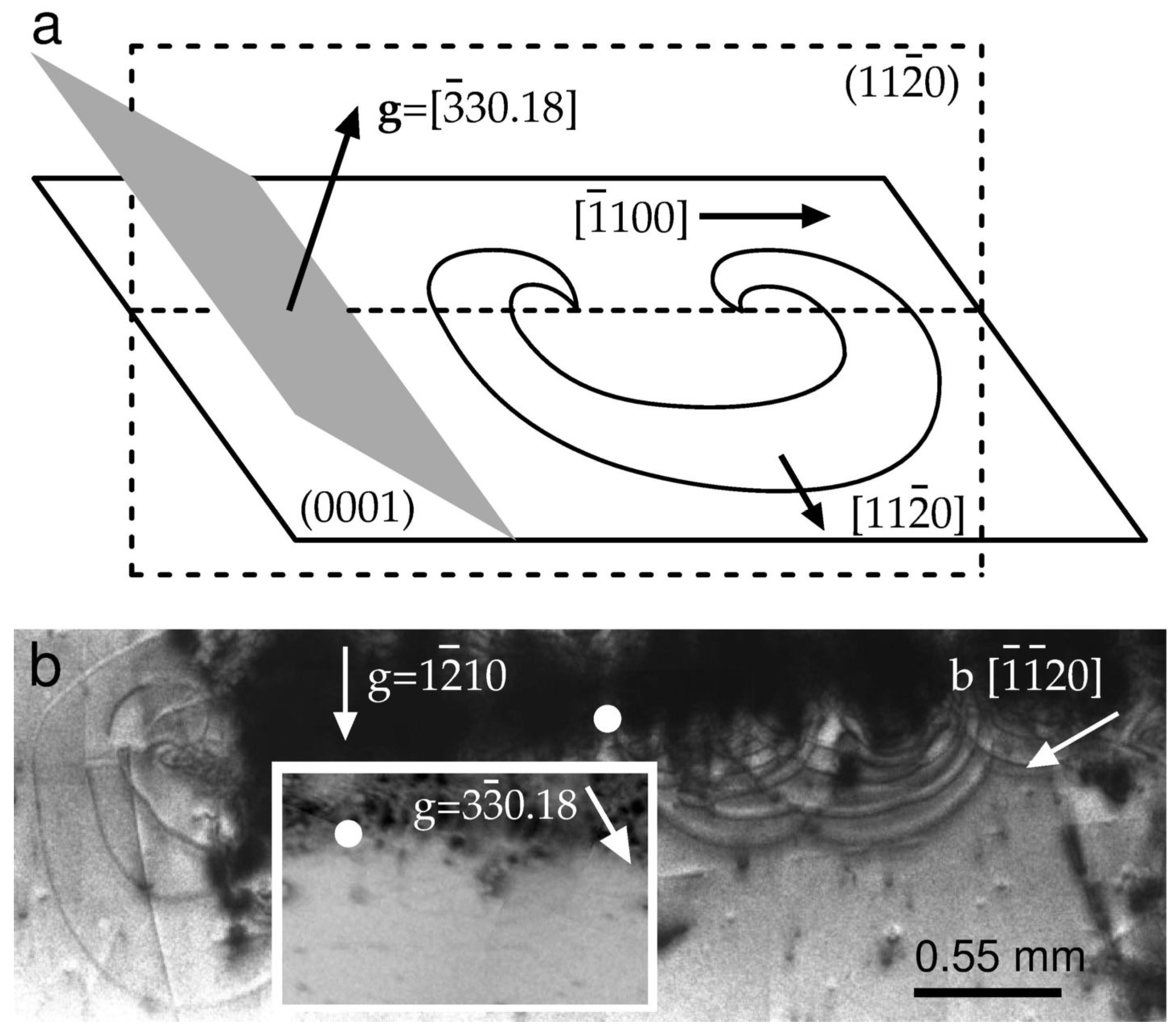
The front view of the sample is schematically represented in
Figure 1a. The arrow located in the neck portion is parallel to the direction of growth [
]. In the sketch, the circle and box refer to the places imaged by SR XRT and PCI, respectively.
Figure 1b shows a high-speed image taken on a VHR CCD detector. Features of the defect density and distribution were quickly visualized within ~2 × 10
−3 s. The following characteristics were visible. First, the rows of dislocation pileups were parallel and perpendicular to the growth direction of the ribbon. Second, the pileups consisted of tangles associated with some dislocation sources. The number of the sources eventually increased with increasing distance from the seed.
Figure 1c,d show topographs taken with Kodak M100 fine-grain film. In high-resolution images, dense tangles were formed by curved lines that were reminiscent of dislocation semiloops. To find basal dislocations in the ribbon, a representative configuration should be revealed by a topograph taken in any {
} diffraction plane. Such a topograph of a (
) reflection is shown in
Figure 1c. The contrast arising from pileups labeled A, B, and C stood out strongly. The rows with high dislocation density were surrounded by a relatively low dislocation density, which made it difficult to assess an average defect density.
To determine whether a particular slip pattern dominated, the contrasts in the g = and g = 00018 reflections were compared. We noticed that some contrasts visible in (c) were absent in the 00018 reflection (data not shown). To understand the variations in dislocation visibility, recall the visibility rules. Purely screw dislocations were invisible when the condition g·b = 0 was satisfied, where b is the Burgers vector. For the case of purely edge dislocations, the visibility was least when the conditions g·b = 0 and g·n = 0 were satisfied simultaneously, where n is a normal to the slip plane.
First, consider in detail those semiloops that expand away from the big pile labeled B in
Figure 1c. The images of semiloops are shown enlarged in
Figure 2b. The inset shows another reflection of the same area. The white circles indicate the same location on both of the topographs. The semiloops are visible in the
g1 =
reflection but invisible in the
g2 =
reflection; therefore,
g2·
b = 0, and the Burgers vector
b of the semiloops is in the [
] direction. In addition,
g·
n = 0 because
b lies on both the (0001) and (
) planes.
A schematic representation of the semiloops along with the (
) reflecting plane is shown in
Figure 2a. The projection of
g =
on the [
] direction shortens the length of
g by a factor of cos 62° (i.e., by 0.5):
gproject = 0.74 Å. A scalar product
g·
b equals 0,
3, and
3 for the
b vectors
1/3 [
],
1/3 [
], and
1/3 [
], respectively. Since
g·
b = 0 and
g·
n = 0 are simultaneously satisfied in the
reflection, the dislocation semiloops in
Figure 2a lie on the basal plane and belong to the (0001), [
] slip system.
Second, we notice an imposing group of semiloops on the left of
Figure 2b. The array contains segments of different visibility. However, when the
,
, or
topographs are examined, the semiloops are contrasted for all three reflections. It is reasonable to assume that the array lies on the prism plane (
) perpendicular to the growth direction.
To get an idea of dislocation sources, let us recall that gas voids are nearly always present in sapphire ribbons. Voids are usually observed in thin surface layers located at a depth of about 100 μm [
29]. In the present study, the back reflection geometry was employed to reveal dislocations in a thin slice of the ribbon close to the surface. In order to evaluate the observable depth
tobs. of dislocations, we used the relationship between
tobs. and the absorption depth
tμ [
30,
31]. For low-absorbing crystals, the dislocation visibility in the back reflection was mainly determined by
tμ with the assumption that the reflected intensity of the X-rays fell down to 10% of the incident power. Considering both paths of the incident and diffracted X-rays,
tμ is calculated as follows [
30]:
where
μ = 18.147 cm
−1,
ω = 68° is the incident angle, and
θ = 40.3° is the Bragg angle. The observable depth
tobs. = 0.23 mm is about 1/5 of the ribbon thickness.
In the back reflection geometry, the strain fields of dislocations lying deeper in the crystal did not contribute significantly to the image. However, when the upper limit of the dislocation density of about 106 cm−2 was reached, the overlap of the dislocation strain fields resulted in a darkening of the region near the dislocation sources. The intensity increase was due to the strong reflectivity of a defective crystal. Interestingly, as images of basal dislocations faded in the reflection, some features became noticeable. Only features with a characteristic size of tens of microns were detected. We can suggest that when a void is large enough, it creates diffraction contrast caused by a change in thickness. As we will see later, oversized voids can merge into cavities.
Note that sources emitting dislocations on the basal plane of the sapphire were proved to operate as Frank–Read sources to emit basal dislocations [
32]. Our topographic analyses revealed basal dislocations with the [
] Burgers vector direction. Dislocations with the (
) prismatic slip plane were also observed. Those dislocations, which gave rise to pileups labeled A, B, and C, stood out strongly in all the obtained topographs. They might have had Burgers vector directions in the basal and prism planes. No experimental evidence of a predominant slip system in the specimens under consideration was found. Finally, in
Figure 1 the [
]—line-direction rows marked with arrows in (c) disappear in (d). These tangled dislocations, which are rendered invisible by the use of the back reflection, might lie deeper than the penetration depth of the X-rays.
3.2. Inhomogeneities
In the present work, micro-inhomogeneities in sapphire ribbons were revealed by the PCI method. Compared with optical microscopy, which is limited to thin slices due to the reduced focus length, the PCI technique provided high-quality images in thin and thick specimens. In the lensless scheme, a nearly parallel SR beam was used together with a pixelated detector. The spatial resolution of the image was related to the pixel size. When an optical lens magnified the image contrasts onto the CCD, the pixel-to-object size ratio was reduced. As a consequence, the FOV became smaller. An experimenter registered only a small fragment of the specimen shown by the detector. Eventually, the fragments could be assembled into a map up to several centimeters in size.
A topograph was recorded at a magnification of unity. The FOV size was shaped up due to slits, beam conditioners, and natural angular collimation of SR. The topographs were subsequently enlarged optically. In order to compare the topographs and the phase contrast images to find common features, a correct scaling needed to be determined. The scale showed a correlation between the topographic distances and the number of pixels in a digital phase contrast image. We emphasize that in the far-field conditions, the phase contrast image had a larger size compared with a small object. We further emphasize that far-field patterns were formed at rather small distances from a micro-object to the detector. Therefore, an inverse problem solution was necessary. Yet, it was always possible to measure large lengths and neglect the relative error.
Figure 3 contains the same region of the ribbon imaged by XRT (a) and PCI (b) methods. The small spots that look darker than the background in (b) can be inclusions, generally formed during the growth process. Impurities in the melt, e.g., molybdenum (Mo) from the Mo shaper, are captured by the crystallization front [
33]. We observed inclusions mainly in the neck portion. To our knowledge, the impurity effects on the generation of dislocations in the sapphire ribbons were not observed, and inclusions of foreign phases were not considered here. The gas void images in
Figure 3b have a simple structure consisting of a black ring around the edge and a light color in the middle. Despite the fact that the distribution of large voids can be controlled by a number of growth parameters (see, e.g., [
13,
14,
16]), a microvoid is still an extremely interesting object of research. There are very few works on the quantitative characterization of microvoids in sapphire crystals using X-ray imaging techniques. The present article fills this gap.
Several features are apparent in
Figure 3: the tangles of dislocation semiloops labeled D, E, and F (a); the small voids of circular shape; and the groups of voids (b). In addition, a sparse distribution of inclusions between the voids and the as-grown surface relief is shown in (b). The dashed lines are located at the same distance from the seed. A direct comparison of the voids (b) and dislocations (a) shows that the voids were very much like the dislocations in their distribution and location. One can conclude that the voids were the cause of the dislocations.
Previous XRT experiments on sapphire ribbons were carried out in defective regions when the lattice distortion was high [
16,
17]. The nucleation centers were not visible because of an increased background intensity occurring when a crystal was imperfect. Unfortunately, the Bragg diffraction contrast was not adequate for studying the nature of defects, when the overlap of images prevented a meaningful interpretation. On the contrary, the PCI confirmed the assignment of the nucleation centers to gas voids. The relaxation of thermal stress began with the formation of glide dislocation semiloops at the voids. The same pattern was repeated further in the direction of growth.
A small scale of the topograph in
Figure 3a allows seeing almost the entire specimen area where defects were formed at the early stage of the ribbon growth. Compared with the topograph, the scale of the phase contrast images was larger. The same observable area is shown in
Figure 3b and
Figure 4. Each image was taken while looking down the growth axis from the seed. The images were connected according to the levels marked with dashed arrows. The distribution of gas voids was noteworthy: they were grouped and distributed across the width of the ribbon.
Consider first the sequences of the voids located between the left and the right of
Figure 4. They are labeled D and E. The narrow gap between D and E is followed by a wider one. On the right, one sees some small voids (labeled F) running from the top to the bottom of the gap. A very similar motif can be found in the topograph below the dashed lines. D, E, and F denote rows of tangled dislocations (
Figure 3a). Rows D and E, which lie across the ribbon width, are followed by row F running in the direction of growth. According to their size, the tangles were presumably generated by the larger (horizontal) and smaller (vertical) groups of voids.
Farther from the seed, the sequences of voids began to form in parallel to the direction of growth. The voids became closer, so that the SR beam, passing through the specimen, intersected pairs of voids. Such closely located configurations are shown in the inset in
Figure 4. Under the action of thermal stress, voids can interact and merge. The coalescence can lead to the transformation of the shapes. Our observations indicated that the distortion of spherical shape proceeded gradually due to some changes in the growth conditions. The nature and evolution of non-spherical voids still remain unclear. In-depth understanding of this phenomenon requires the analysis of void sizes.
3.3. The Size of the Gas Voids
If an X-ray beam passed through a sample with inhomogeneous thickness and/or density, the wave field acquired an additional phase shift, variable in the direction perpendicular to the propagation direction. A void entailed a phase shift proportional to
s Δδ, where
s is the void thickness, and δ is a decrement of the refraction index
n = 1 − δ of materials. In the hard X-ray range (
E > 6 keV), the phase shift of a coherent SR beam could be detected when the sample thickness changed from at least ~0.1 μm to several microns. In the near field, i.e., at a short distance
z from the sample, the intensity oscillations were simple in shape but varied in amplitude and period. For a larger
z, the sinusoidal variation in the intensity specific to Fresnel zones was formed. The sizes of the microvoids could be determined using computer simulations. To make certain that the obtained cross section diameters are correct, one has to register and fit the images of the same void at some different distances
z (see, e.g., [
34,
35]).
As for spherical voids, their simulations were carried out in an earlier work [
36]. Unlike these, we chose an experimental picture that showed the overlay of two voids located at a certain distance from each other. To our knowledge, the fitting of such configurations has not been reported.
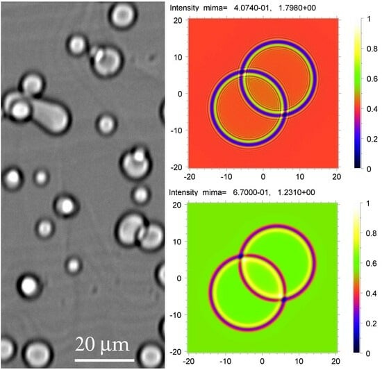
Figure 5 shows the phase contrast images recorded on the CCD at the distance
z1 = 1.5 cm (a) and
z2 = 20 cm (b). We note that the width of the void boundaries changed and became larger with the distance
z, which was a consequence of the interference nature of the images. The boundaries did not overlap, so the void diameter could be roughly estimated from the image pixels. The preliminary estimates showed that the average diameter at both distances
z1 and
z2 was approximately 60 pixels. For a given pixel size of 0.325 μm, we obtained ≈20 μm. One can see that the diameters of the voids were greater than the diameter of the first Fresnel zone 2
r = 2(
λ z)
1/2, which was equal to 2
r1 = 2.2 μm and 2
r2 = 8.1 μm at distances
z1 and
z2, respectively. The width of the edges increased with the distance
z, but the average diameter did not change.
The inline phase contrast setup did not allow an evaluation of the depth of a void in a sapphire ribbon. It was, therefore, impossible to know the distance between voids since this distance did not influence the simulated images. The sizes of voids can be different. Below we will consider a model applicable to a specific case, namely, two identical spheres with a diameter of 20 μm. Their centers were shifted diagonally by 8 × 2
1/2 = 11.3 μm. The calculation was performed by the XRWP (X-ray Wave Propagation) program [
37]. The program calculated a series of two-dimensional patterns using formulas of the phase contrast theory of three-dimensional objects. The wave propagation through a substance, in which the electron density varied, was described by the transmission function of the object. Since the object containing voids was not uniform, the thickness was a variable function of the coordinate. Propagation in a free space was calculated according to the Huygens–Fresnel principle as the convolution of the wave function with the Fresnel propagator [
1]. The convolution was computed through the Fourier transform method. The fast Fourier transformation (FFT) method was applied [
38].
Prior to describing the results of the simulation, it is necessary to emphasize that for the imaging techniques, the recorded image resulted from a convolution of the sample response and the detector characteristics. In addition, the experimental pattern depended on the size of the SR source. A good approximation of the source is the model in which every point of its transverse size radiates independently, and the radiation intensity obeys the Gaussian law, i.e., the source may be characterized by the half-width of the Gaussian function. The structure of an image also depended on statistical and instrumental noise. The signals recorded using a CCD were superimposed on a background. When the calculated pattern was compared with the experimental one, it was necessary to normalize the latter. In order to obtain a good fit between the simulation and the experiment, the constant background must be subtracted.
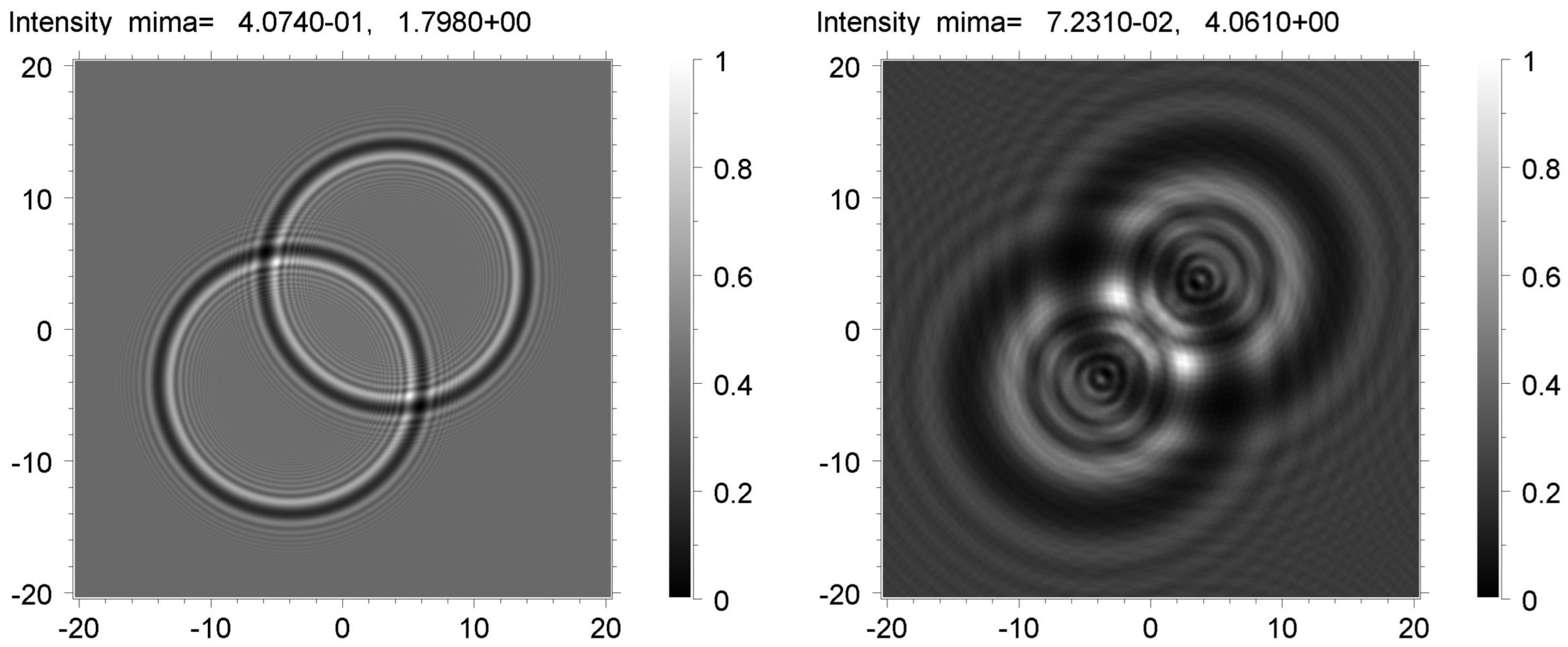
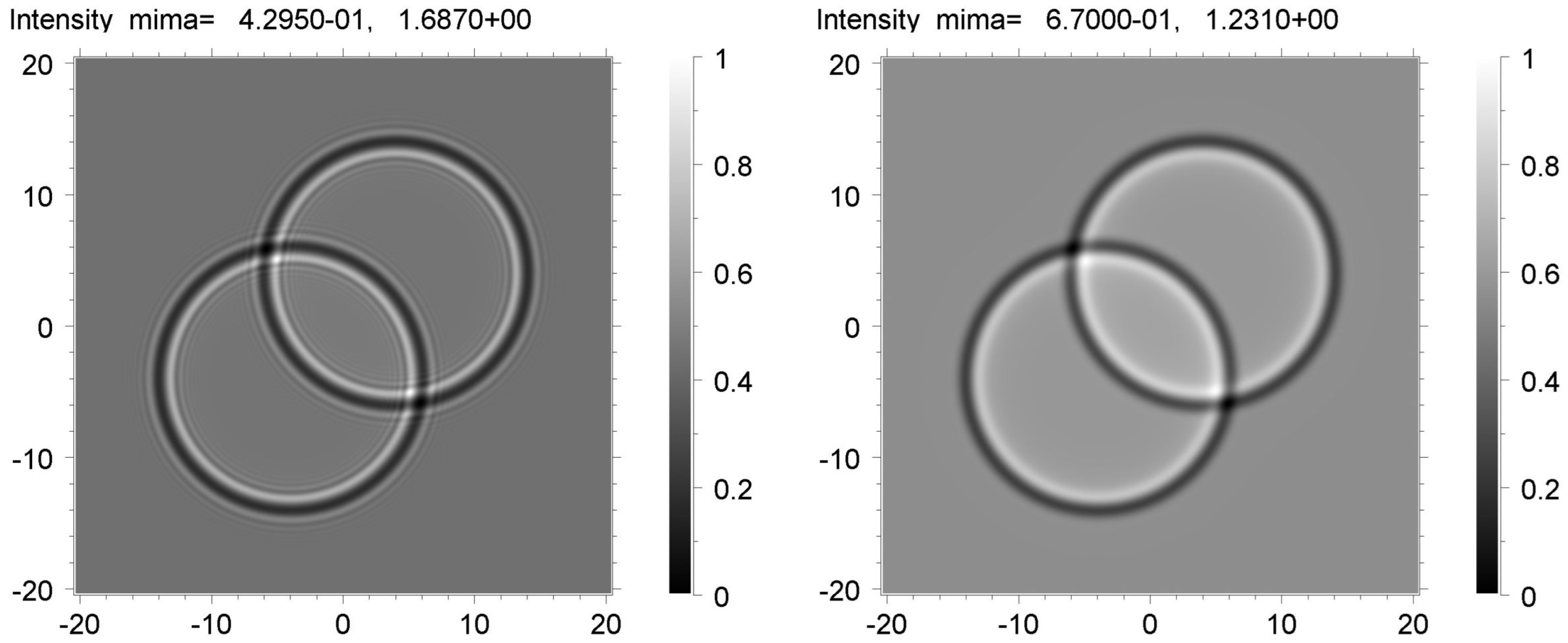
At the initial stage, the simulation was carried out for fully coherent monochromatic radiation emitted by a point SR source and recorded using an ideal detector. The program calculated theoretical images, which contained sharp peaks of high intensity. The sample area containing these peaks was very small. A comparison of the image on the left in
Figure 6 with the image on the right shows that the effect became more pronounced at the long distance
z2 = 20 cm. Prior to making comparisons with experimental images, the calculated images were averaged. We employed the convolution of the two-dimensional intensity distribution on the detector with a two-dimensional Gaussian function. Since the asymmetry of the directions along and across the SR source was not noticeable, we used the symmetric two-dimensional Gaussian. The convolution was performed for different values of the full width at half maximum (FWHM), which were the same in two directions.
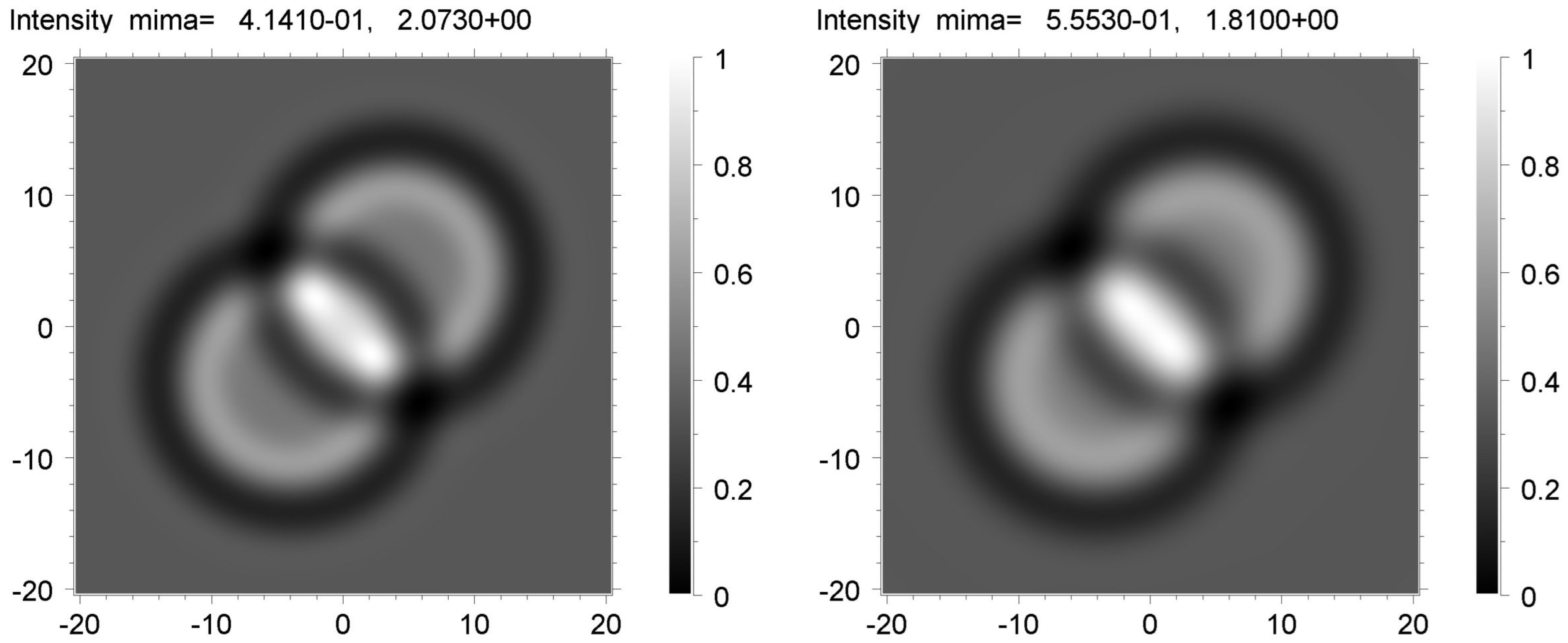
The best fits to the experimental data were selected.
Figure 7 shows the averaged theoretical images of the voids calculated for the distance
z2 = 20 cm using the convolution with the Gaussian of the FWHM = 3 μm (left) and 4 μm (right). Let an optimal Gaussian FWHM be 3.5 μm. We emphasize that the value of FWHM must depend on the distance
z. There were, therefore, good reasons for the automatic variation in two parameters during the simulation: the value of the FWHM and the sample-to-detector distance
z. If we assume that the averaging occurred due to the source size, a decrease in
z by a factor of 13.3 caused a decrease in FWHM by the same factor. Thus, we might expect that for the distance of 1.5 cm, an optimal FWHM was 0.26 μm.
However, this effect is not observed in
Figure 8, which contains the image simulations by FWHM = 0.26 μm (left) and 1 μm (right). The theoretical image on the right exhibits the distinctive effect of a large FWHM. It is more consistent with the experimental picture than the image on the left in
Figure 8. To sum up, the averaging arising from the source size was observed but only to a certain extent. The given example clearly shows that imaging detectors and other aspects of the experimental procedure (including a sample vibration) should not be neglected when extracting quantitative information from an image.


 ,
, 


