3.1. PbSn Solder Properties Experimental Analysis
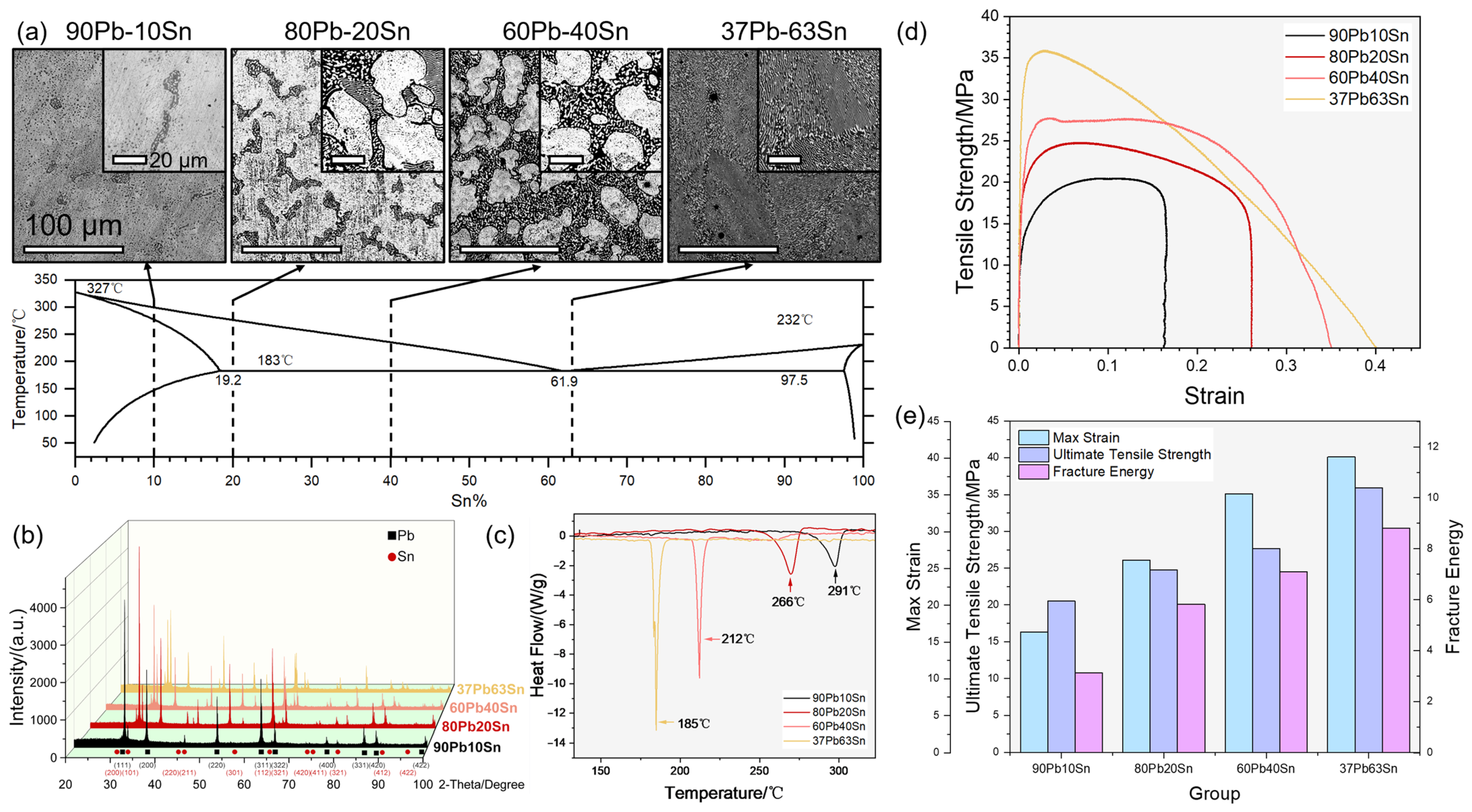
In this section, Pb-Sn solders with different chemical compositions were systematically studied. The four different solder alloys were fabricated as depicted in
Figure S1a. Protection with molten salts helps to avoid severe oxidation, maintaining the ratio of two elements in the melt. As shown in
Figure 1a, the microstructures changed with the chemical compositions of the solder alloys. According to the eutectic phase diagram of Pb and Sn, both elements exist in solid solution (α-Pb phase or β-Sn phase) or eutectic (Pb:Sn = 38.1:61.9). Larger and inset images showed millimeter- and micrometer-scale perspectives, respectively. As the Sn content rose from 10% to 63%, the dark eutectic of the white α-Pb phase gradually took place in the Pb-Sn cast condition microstructures. Due to the proximity of the Pb37Sn63 solder to the eutectic, the microstructure was completely occupied by random-oriented lamellar eutectic. Correspondingly, the XRD patterns in
Figure 1b show the decrease in α-Pb phase signals (black square) and the increase in β-Sn phase signals (red circle). In
Figure 1c, significant changes of heat flow mark the violent melting of the alloys. Due to the inclusion of various microstructures with different melting points in alloys, they have a melting range rather than a melting point, where solid and liquid coexist. The measured “melting point” of the four samples were 291 °C, 266 °C, 212 °C and 185 °C (from 90Pb10Sn to 37Pb63Sn), respectively, each corresponding to a melting range. To access their mechanical properties, the samples underwent tensile tests, depicted in
Figure 1d,e. Elastic deformation, uniform plastic deformation, local concentrated plastic deformation after necking and final fracture were observed during the tests. Among the four as-cast Pb-Sn alloys, 37Pb63Sn alloy showed the best performance in the tensile test for its maximum deformability and absorbed energy before final fracture. The excellent mechanical properties of the alloy were largely attributed to its eutectic microstructure, which showed small interlayer spacing and fine grains. Furthermore, the uniform synchronous deformation of the refined grains made the eutectic solder alloy less prone to stress concentration, delaying the initiation and propagation of cracks. Therefore, the 37Pb63Sn solder had both good plasticity and tensile strength. As the Sn content decreased, the max strain, ultimate tensile strength and fracture energy synchronously declined. Moreover, the fracture mode changed from ductile fracture for 37Pb63Sn to brittle fracture for 90Pb10Sn at the end stage of their stress–strain curves. Due to the lower melting point and obvious performance advantages under room temperature, the 37Pb63Sn was considered the mostly commonly used solder alloy containing Pb.
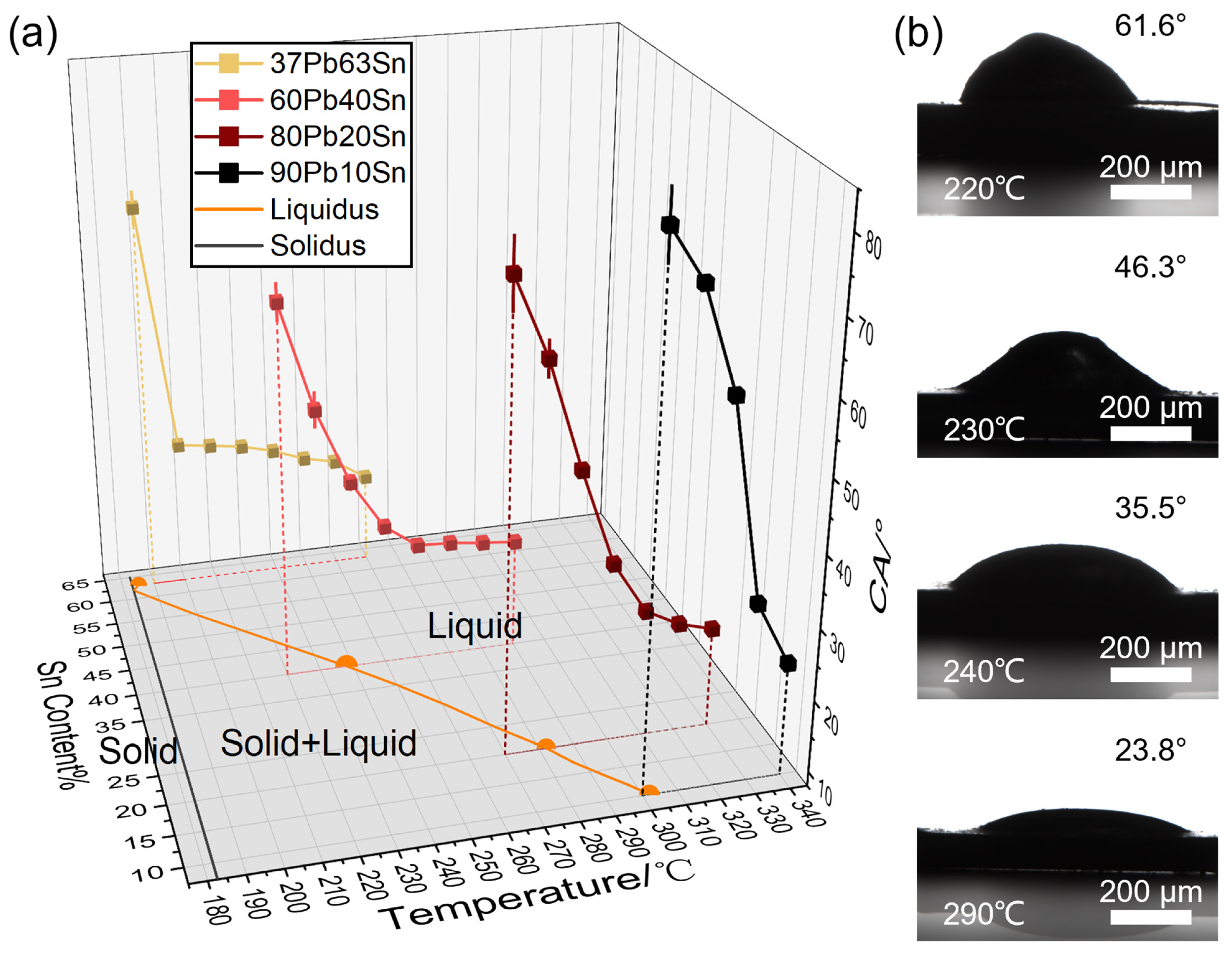
In
Figure 2, the high-temperature wettability to the Ni substrate of the four solders is systematically shown. The alloys melted in the temperature ranges between the liquidus and solidus, and their viscosity decreased as the rate of liquid phase increase during the heating process. When the alloys started to wet the substrate and showed contact angles, they were not fully melted (under the liquidus). In
Figure 2a, the contact angles decreased with increasing temperature for each alloy, but the lowest contact angle was above 20°. When the temperature was close to their melting point, the receding rate of contact angle was much higher. During synchronous heating of the four solders, 37Pb63Sn first wetted the Ni substrate and then spread, ensuring a good mechanical and electrical contact, while the solders with high-Pb content required much higher ambient temperature for good welding, which consumed more energy and triggered potential failure in applications. The solders wetted the Ni substrate well at 20–40 °C above their melting point regardless of their compositions, proving the excellent welding performance of Pb-Sn alloy. In
Figure 2b, the elevating temperature facilitated the spreading of Pb60Sn40 solder on the Ni substrate. Before the measurement, the polishing of the Ni substrate, purification of solder alloys and inert gas protection was necessary to prevent interfacial metal oxides from interrupting the wettability measurement.
In the electronics industry, high-Pb solder has shown its higher reliability over 37Pb63Sn solder, making it commonly used in products for aerospace and military purposes. In the identically applied reliability tests, the superb stability of high-Pb solder was fully revealed. The temperature circulation test examined the ability of the device to withstand extreme high and low temperatures, as well as the impact of alternating temperature changes. The high-temperature storage test verified the reliability and quality of devices that can withstand test conditions throughout their entire lifespan, highlighting defective products with initial failure. The multiple reflow test determined whether the device could withstand the thermal effects generated during the welding process and evaluated the impact of reflow effects. The cross-section SEM images of the solder bumps are shown in
Figures S3–S5 sequentially. The inset images show the full view of the solder bumps, while the large image shows the interfaces between the solder balls and the substrates. During the reliability tests, the IMC growth and development was crucial to the mechanical strength. The IMC thickness was measured from the SEM images and is organized into diagrams in
Figure 3. The high-temperature procedure in the reliability tests greatly accelerated atomic diffusion, enabling the rapid formation of IMCs. Obviously, as the experiment progressed, the IMCs gradually thickened, and the growth rate declined, showing linear positive correlation The IMC thickness was linearly correlated with the square root of temperature cycles, reflow cycles and storage time, respectively. Considering that the atomic diffusion rate was also proportional to the square root of time (t
1/2), the determining factor of IMC formation was bulk diffusion for all solders. The thickness and growth rate of IMCs was lower in solder bumps with higher Pb content, indicating that Pb effectively inhibited the growth of IMCs. Additionally, Pb also greatly affected the IMC morphology evolution. For high-Pb content solders like 90Pb10Sn, the initial planar IMCs was about only 0.5 μm in thickness and the IMCs grew slowly in the long-period reliability tests. After 1000 temperature cycles, 20 reflows or 1000 h high-temperature storage, the IMCs’ morphology slightly roughened, showing a clear trend of scalloping. Pb60Sn40 was a typical medium-temperature solder with moderate Pb content. The IMCs of the as-prepared Pb60Sn40 bumps were scallop-shaped and further developed into bamboo-shoot-shaped columns and crystals, especially in multiple reflow tests. When the Pb content was lower, such as in Pb37Sn63 solder, the bamboo-shoot-shaped IMCs grew quickly and intruded into solders with less difficulty, forming a more complex and disordered interface. The interfacial strength was low, leading to the easy dewetting and detachment of solders and final failure of the package. This phenomenon was particularly evident in reliability tests with strong convection like the multiple reflow tests. In
Figure S3, clear interfacial crack across the IMCs can be observed in 37Pb63Sn solder bumps after 1000 temperature cycles. In the high-temperature storage experiments, IMCs tended to grow in layers with a much weaker tendency to form rougher interfaces. In summary, the IMC thickness increased and the IMC morphology became uneven with increasing Sn content. Considering the thickness and morphology of the IMCs, flip chip devices with 90Pb10Sn bumps have the best reliability under the same reliability test conditions.
The mechanical properties of the solder bumps were greatly related to the interfacial microstructures. Shear force applied on the flip chip detached the mounted chip from the substrate, leaving residual solder alloys. Observation of the residues shown in
Figure 4a,b suggested that the 37Pb63Sn solder joints broke at the solder–substrate interface while the other two broke inside the solder ball, showing a crack mode transition from ductile fracture to brittle fracture with decreasing Pb content after identical reliability tests. Due to the prosperous growth of bamboo-shoot-like IMC microstructures, the solder–substrate interface bonding was severely cut and weakened by brittle IMCs.
Further observation of the solder–substrate interface revealed its microstructures and chemical compositions, as shown in
Figure 5. On the electroplated millimeter-scale Ni layer, the solders wetted well and formed IMCs composed of Sn and Ni. The atomic concentration of Ni decreased in the solder. The main component of IMCs was Ni
3Sn
4 according to the atomic ratio of Ni and Sn, while other components, including Ni
3Sn
2 and Ni
3Sn, existed close to the Ni layer, owing to the diffusion limitation. The chemical composition in the solders were not uniform due to the α-Pb phase and β-Sn phase with different element ratios.
3.2. Reliability Optimization Based on Microalloying
In the following section, starting from the first-principles calculation of the Ni3Sn4 growth process and doping effects of other elements, the long-term reliability of flip chip was evaluated with both experimental and simulation methods. All energy calculations were based on the Cambridge sequential total energy package (CASTEP, GGA-PBE functional) module and the valence band electrons of Sn (5s25p2), Ni (3d84s2) and Cu (3d104s1), Ge (4s24p2) were calculated using the Vanderbilt ultrasoft pseudopotential method.
The Ni
3Sn
4 cell is shown in
Figure 6a, in which six Ni atoms and eight Sn atoms constituted this monoclinic cell, belonging to the C2/m space group. Lattice constants included a = 11.952 Å, b = 3.991 Å, c = 5.131 Å and β = 104.84°. There were two types of Ni and two types of Sn atoms in the cell, occupying positions marked as 2a and 4i and 4i
1 and 4i
2, respectively. The atomic coordinates are organized in
Table 1.
For Ni
3Sn
4-based IMCs, the diffusion process was mainly related to bulk diffusion, as discussed above. The vacancy diffusion mechanism was considered dominant because the atomic radii of Sn, Pb, Ni and Cu in the transition element region were close (as shown in
Table S2), making interstitial diffusion difficult for them. The exchange mechanism was sparsely observed owing to its high activation energy and thus was not considered in this study.
The Ni
3Sn
4 cell with four kinds of vacancies was considered as depicted in
Figure 6b: Sn(4i
1), Sn (4i
2), Ni(2a) and Ni (4i). In this part (vacancies calculation using Geometry Optimization module), the parameters are shown in
Table S1. The difference between the complete cell with no vacancy and the cell with vacancies was the formation energy of vacancies, calculation results of which are shown in
Table 2, indicating that the formation of Ni vacancies was much easier than those of Sn. Additionally, the atomic radius of Ni (1.24 Å) was much smaller than that of Sn (1.58 Å), and the diffusion distance for Ni was also smaller than that of Sn in the cell. Therefore, Ni was considered the main diffusion element (Ni into PbSn solder but not Sn into Ni substrate).
To further determine the main diffusion channels in Ni
3Sn
4 structures, the TS Search module was applied to calculate the transition state of Ni atoms among these vacancies in the supercell constructed in
Figure 6c to facilitate the linear/quadratic synchronous transit (LST/QST) calculation. All the parameters are listed in
Table S3, and the exchange energy barriers between Ni atoms and Ni vacancies are all listed in the
Table 3.
Obviously, the 1~0 diffusion was much easier than other diffusion types. As shown in
Figure 6d, for Ni atoms in 4i positions, they diffused along a zigzag pathway along the [1 0 0] direction, while Ni atoms in 2a positions first migrated to 4i positions via other diffusion paths and then diffused like the Ni atoms in 4i positions. In summary, the main diffusion channels in Ni
3Sn
4 were along the [1 0 0] direction according to the calculations above.
The doping of other elements causes lattice deformation, which may interfere with the Ni diffusion procedure. The cell formation energy after Ge/Cu substitution at the four positions in the 1 × 2 × 2 supercell was considered in
Table 4. The lowest cell formation energy of Ge and Cu were Ge-Sn (4i
2) substitution (−0.25943 eV) and Cu-Ni (4i) substitution (−0.26015 eV), respectively, but the cells after doping were all less stable than the pristine Ni
3Sn
4 cell, indicating that the lattice deformation caused by doping elevated the lattice energy.
As the Ni atoms mainly migrate via the 1~0 diffusion along the zigzag pathway along the [1 0 0] direction in the Ni
3Sn
4 IMCs, the doping elements which inhibit 1~0 Ni diffusion will further lower the growth rate of the IMCs, preventing the solder bumps from failures caused by IMC overgrowth. The [1 0 0] diffusion channel is dependent on the 1~0 diffusion path, and the exchange energy barrier of the path is directly related to the cell structure, which underwent deformation after doping. In
Figure 6e,f, the doping of single Ge or Cu atoms in the 1 × 2 × 2 supercell is illustrated. The calculation results of the Ni-vacancies exchange energy barrier after doping are organized in
Table 5 and
Table 6. After the single atom doping in the supercell, the concentrations of Ge and Cu were 1.4 wt% and 1.22 wt%, respectively.
From the calculation above, the 1~0 diffusion was still much easier than other possible paths, suggesting than the 1~0 diffusion was dominant after doping. Comparison of the minimum exchange energy barrier with Ge/Cu doping and the pristine Ni3Sn4 cell showed that the Ge substitution increased the required energy for Ni-vacancies exchange while the Cu substitution facilitated the Ni-vacancies exchange; in other words, Ge was a potential IMC growth inhibiter while Cu doping accelerated the IMC growth rate.
To evidence the repression of Ge doping to the IMCs of PbSn solders, Pb59.97Sn40Ge0.03 solder (the concentration of Ge was 0.013 wt%) was fabricated using the same method shown in
Figure S1a and compared with Pb60Sn40 solder without Ge doping in all three reliability tests, and the results are shown in
Figure 7.
After 1000 temperature cycles, the Pb59.97Sn40Ge0.03 and Pb60Sn40 bumps maintained their interconnection structures and no obvious cracks were observed, but the IMC layers were much thicker during the test. The IMC layer was planar with Ge doping, while the IMC layer without Ge infiltrated into the solders fiercely when the temperature cycles exceeded 700. In the multiple reflow test, the initial planar IMC layers were both thin for the two samples, but the IMCs in the solder with Ge doping propagated more slowly. When the reflow cycles reached 20, the IMCs in the Pb59.97Sn40Ge0.03 solder showed a scallop-like shape while the IMCs in the Pb60Sn40 solder changed to a bamboo-shoot-like morphology, which was more brittle and easier to break under local stress. During high-temperature storage, the changes in IMC morphologies were relatively smaller. As the storage time increased from 100 h to 1000 h, the IMC layer maintained planar growth for Pb60Sn40. The IMC morphologies in Pb59.97Sn40Ge0.03 solder changed from coarse front to planar surface, exhibiting a roughness decrease. The spontaneous recovery from a rough interface to planar growth mode should be attributed to the growth kinetics and interface thermodynamics. At first, the IMC growth rate was higher, so the scallop-shaped IMC layer was more favorable. However, its ragged interface with the solder contained higher surface energy than the planar interface, driving the IMC–solder interface to transform into a planar shape. In the other two reliability tests where environment conditions changed continuously, similar phenomena were rarely observed.
According to the statistics of the IMCs thickness of the solders shown in
Figure 7d, the IMC thickness in Ge-containing solders changed more slowly than Ge-less Pb60Sn40 solders, implying that the IMC growth was greatly suppressed by the trace Ge addition. The Ge-containing solders were less influenced by the failures caused by IMC growth, showing a better reliability and longer lifespan in all three reliability tests.


 ,
, 


